Book Appointment Now

How a hybrid PCB stackup pairs low-loss laminates with FR-4: where the material split goes, how lamination changes, and when the hybrid build pays off.
Hybrid PCB Stackup Guide: Mixed Dielectric Materials, Cost and Uses
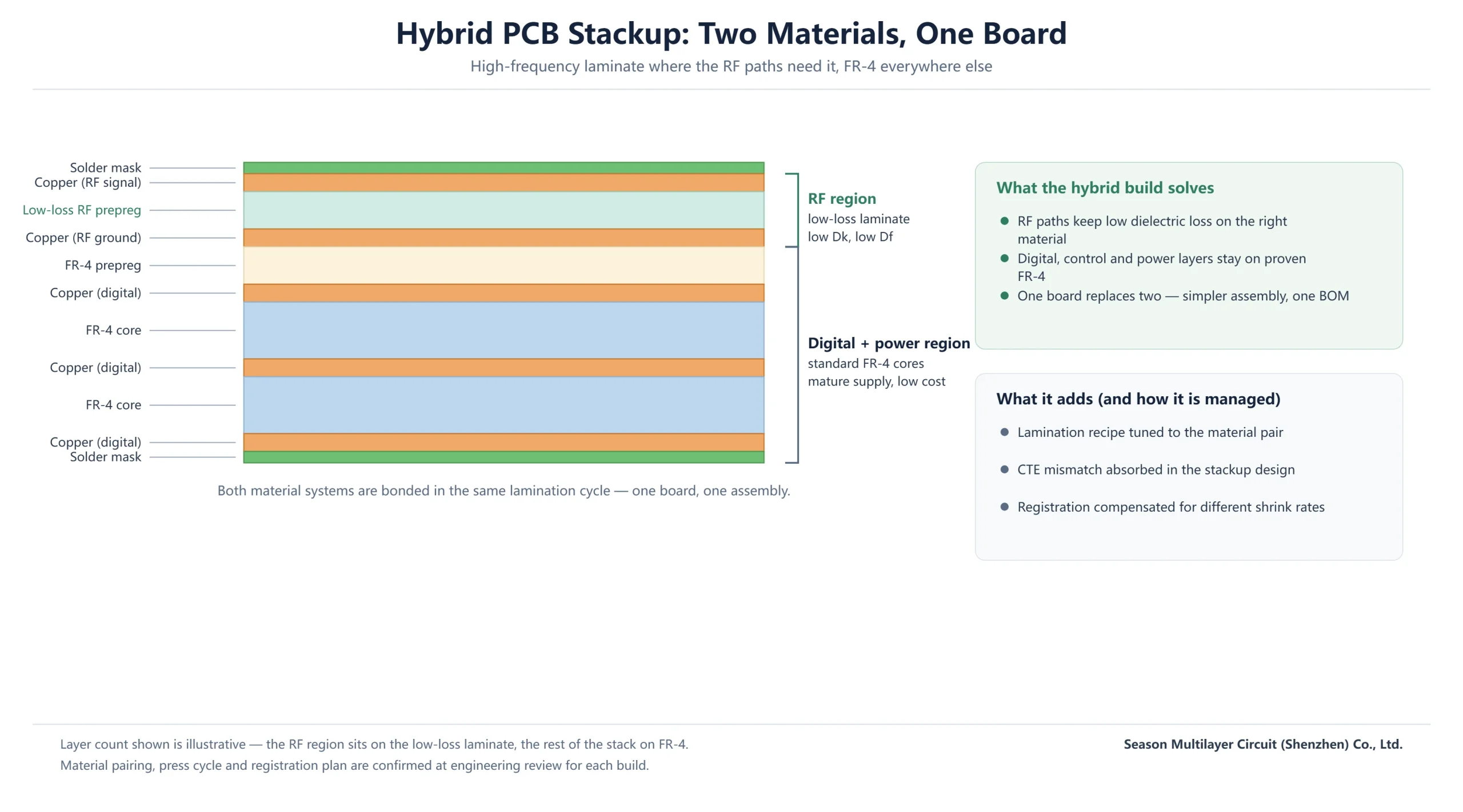
RF sections want expensive low-loss laminates; digital, control and power sections run happily on FR-4. Paying high-frequency prices for the whole board just to serve a handful of radio nets is the fastest way to blow up a hardware budget — but routing those nets onto a second board creates assembly, reliability and supply-chain problems of its own. A hybrid PCB resolves the trade-off inside one board: low-loss material where the radio paths live, FR-4 everywhere else, laminated together as a single build.
This guide is written from the fabricator side. It covers what a hybrid stackup actually looks like, which material combinations are common, how lamination, drilling and registration differ from a conventional build, and where the cost sits once the press cycle is accounted for. If you are weighing a full high-frequency board against a mixed build, the tables below give you the decision criteria without the marketing gloss.
Table of Contents
- What Is a Hybrid PCB?
- Why Mix Dielectric Materials on One Board?
- Common Hybrid PCB Laminate Combinations
- Hybrid PCB Stackup Design Rules
- How a Hybrid PCB Is Laminated, Drilled and Finished
- Hybrid PCB Cost Trade-offs in Real Builds
- Where Hybrid PCBs Are Used
- A Pre-Quote Checklist for Hybrid Builds
- Quality Controls That Decide Hybrid Yield
- FAQ
- Get Your Hybrid Stackup Reviewed Before You Release It
What Is a Hybrid PCB?
A hybrid PCB is a single board built from two or more dielectric material systems with different electrical properties. In the typical multilayer case, the outer RF layers and their immediate dielectric are made from a low-loss, low-Dk laminate, while the inner digital and power layers use standard FR-4 cores and prepreg. The two systems are bonded in one lamination cycle, so the finished board behaves — and is assembled — exactly like a conventional multilayer PCB.
The approach is also called mixed dielectric or mixed lamination construction. The defining idea is zonal: each circuit region gets the material whose properties it actually needs. Antenna feeds, filters and PA outputs get tight Dk control and low dissipation factor; microcontrollers, memory and power regulation get the mechanical robustness and mature supply chain of FR-4. Neither region subsidises the other’s material.
Why Mix Dielectric Materials on One Board?
The physics is straightforward. Signal loss in a dielectric scales with frequency, so the gap between a standard FR-4 (dissipation factor around 0.020 at 10 GHz) and a quality low-loss laminate (0.002–0.004) becomes decisive once radios move into the multi-gigahertz range. At 28 GHz, moving the RF paths from FR-4 onto a low-loss dielectric cuts insertion loss by roughly 30% — the difference between a link that closes with margin and one that needs more PA power, more receive gain, or both.
What the high-frequency layers need from their material:
- Low, stable dielectric constant — typically Dk 2.5–3.5 held to tight tolerance, so impedance and phase stay predictable across the panel
- Low dissipation factor — 0.004 or better at operating frequency, ideally below 0.004 at 10 GHz for millimetre-wave work
- A flat temperature coefficient, so electrical performance holds from cold start to full thermal load
- Uniform Dk in the X, Y and Z axes, because controlled impedance depends on all three
What the rest of the board needs is exactly what FR-4 delivers: mechanical strength for connectors and stiffeners, proven drilling and plating behaviour, a deep supplier base, and stable pricing. Mixing the two materials keeps each requirement paired with the cheapest material that satisfies it — that is the entire commercial argument for the hybrid approach.
Common Hybrid PCB Laminate Combinations
Most production hybrids fall into three families. The workhorse is FR-4 paired with a ceramic-filled low-loss laminate in the Rogers RO4000-class family — the same material system used on our Rogers high-frequency PCB builds. The second family pairs FR-4 with PTFE-based laminates for the highest millimetre-wave frequencies. The third mixes two different low-loss materials, each tuned to a different RF function.
| Combination | Typical use case | Material cost vs an all-high-frequency build |
|---|---|---|
| FR-4 + ceramic-filled low-loss laminate (RO4000-class) | RF front ends, antenna feeds and filters on the RF layers; baseband and power on FR-4 | Roughly 40–50% lower |
| FR-4 + PTFE laminate | Millimetre-wave radios and 77 GHz radar where loss floor matters most | Lower; the saving scales with the FR-4 layer share |
| Two different low-loss laminates | Antenna region on higher-Dk material, feed network on the lowest-Df material | Tuned per region; still below an all-premium build |
| FR-4 + mid-loss laminate | Cost-driven RF designs below ~6 GHz | Smallest premium over all-FR-4 |
The combination choice is not only electrical. Ceramic-filled thermoset laminates laminate and drill much closer to FR-4 than PTFE does, which keeps the process — and the yield risk — closer to a conventional build. PTFE systems bring the lowest loss but need plasma hole preparation and tighter storage discipline. We cover those process differences in the manufacturing section below.
Hybrid PCB Stackup Design Rules
A hybrid stackup succeeds or fails at the material boundary. Every rule below exists because the two dielectric systems differ — in Dk, in CTE, in shrink rate during lamination — and the design has to absorb those differences instead of ignoring them.
Impedance continuity comes first. A 50 Ω single-ended or 100 Ω differential trace that crosses from the low-loss layer into FR-4 territory sees a Dk step, and the impedance steps with it unless line width and dielectric height are re-solved for each region. Field-solver modelling per region, confirmed by TDR measurement on the impedance coupon, is the standard practice — the tolerances we work to are ±10% as standard, ±8% on request, and ±5% where the design justifies it.
Thermal expansion mismatch is the second rule. FR-4 expands roughly 50–70 ppm/°C through the Z-axis while low-loss laminates sit below 20 ppm/°C; every heat cycle works the boundary between them. The stackup answers with CTE-matched pairing, balanced copper distribution, and thermal via arrays under power devices so no single material band carries the stress alone.
| Design parameter | Failure mode if ignored | Typical mitigation |
|---|---|---|
| Impedance across the material transition | Reflections and mismatch at the Dk step | Per-region solver models, TDR-verified coupons |
| Z-axis CTE mismatch (50–70 vs <20 ppm/°C) | Delamination and cracked via barrels over thermal cycling | CTE-matched pairing, balanced copper, thermal via arrays |
| Prepreg selection at the boundary | Voids or weak bonding between dissimilar cores | Prepreg flow and cure matched to both material systems |
| Registration across materials | Layer-to-layer misalignment at the boundary | Shrink compensation per material from measured process data |
| Copper balance across the stack | Warp and twist after lamination | Symmetric copper distribution and stress-relief features |
Acceptance criteria for the finished hybrid board follow the same IPC standards used for any Class 2 or Class 3 build — the mixed construction changes how the fabricator gets there, not what the board has to survive.
How a Hybrid PCB Is Laminated, Drilled and Finished
Preparation separates a hybrid build from a conventional one before the press is even loaded. High-frequency materials are cut and handled in controlled conditions to keep dust and contamination out of the RF dielectric. PTFE-family laminates in particular need disciplined storage — around 22 ± 3 °C and 30–40% relative humidity — because absorbed moisture flashes to steam in the press and shows up later as delamination or voids.
Imaging and lamination carry the critical tolerances. Laser direct imaging holds line width to about ±5 µm, which matters because RF trace geometry is part of the impedance definition. In the press, the lamination cycle is tuned to the material pair: a slow ramp of roughly 2–3 °C per minute lets the prepreg flow and degas before cure, and a staged pressure profile starts low so the material can move, then consolidates the full stack. Cure windows are set per prepreg system rather than borrowed from the FR-4 recipe.
Drilling adapts to the harder dielectric. Feed and speed are re-optimised when the drill crosses from FR-4 into ceramic-filled or PTFE material, and PTFE hole walls need plasma treatment before electroless copper or the plating will not adhere. On builds where through-hole stubs would hurt high-speed nets, backdrilling removes the unused barrel — a step worth flagging at quotation because it adds a pass. Finished hybrids then go through the same AOI, impedance coupon testing and cross-section checks as any multilayer order.
Hybrid PCB Cost Trade-offs in Real Builds
The commercial case for a hybrid PCB rests on where the expensive material actually sits. In a radio board, RF layers are typically a minority of the stack; putting low-loss laminate only where they run cuts the material bill roughly 40–50% against an all-high-frequency equivalent, and total board cost by roughly 25–40% once processing is included. The premium over an all-FR-4 board remains real — it buys back link budget and range that FR-4 cannot deliver above a few gigahertz.
| Build option | Relative material cost | Dielectric loss at 10 GHz | Where it fits |
|---|---|---|---|
| All FR-4 | Baseline (1.0×) | ~0.020 — workable for digital, marginal for RF | Digital, control and power boards |
| Hybrid: FR-4 + low-loss RF layers | Well below all-high-frequency; RF material only where RF runs | RF layers ~0.003–0.004; digital layers unchanged | Mixed RF + digital boards — the majority of radio designs |
| All high-frequency laminate | Highest | ~0.002–0.004 everywhere | Dense mmWave boards where most layers carry RF |
There is also a system-level saving that pure board-price comparisons miss. One hybrid board replaces a two-board assembly: fewer connectors, one placement and reflow pass, one solder-joint reliability budget. On a 77 GHz radar module, keeping antenna, feed network and processing on one mixed-dielectric board with 15%+ better signal reach than an FR-4 equivalent often costs less overall than the separate-board alternative it replaces.
Where Hybrid PCBs Are Used
Base station and backhaul radios were the first large-scale adopters and remain the archetype: massive MIMO arrays pack 64 or more antenna elements onto the RF layers of a hybrid build, with isolation between channels held above 25 dB while the baseband below runs on FR-4. The same pattern repeats in every radio that mixes high-frequency analogue front ends with substantial digital processing.
Automotive radar is the second pillar. A 77 GHz front-end board is a natural hybrid — antenna and feed structures on a low-loss, tight-Dk dielectric, signal processing below on FR-4 — and the approach extends into ADAS sensor-fusion modules where camera and radar electronics share one board. Our radar high-frequency PCB work follows exactly this construction.
Optical and high-speed computing rounds out the field. Optical module carriers put 100G/400G SerDes channels on low-loss dielectric while management circuits ride FR-4, as on our optical module PCB builds; 5G small cells, satellite terminals and test instrumentation all use the same zoning logic wherever multi-gigabit or multi-gigahertz signals meet cost-sensitive volume.
A Pre-Quote Checklist for Hybrid Builds
Hybrid quotes vary more between fabricators than conventional ones, because the lamination recipe and the material pairing are both engineering decisions. Sending the package below turns the first quote from an estimate into a firm number.
- Which layers or regions are RF — net classes or a marked-up stackup drawing
- Target impedance per net class, with the tolerance band the design actually needs
- Preferred laminate system, or the frequency and loss budget so the fabricator can propose one
- Layer count, finished thickness and copper weights per layer
- Surface finish, plus any backdrilling or controlled-depth routing
- Expected volume and delivery, so the lamination approach can be sized to the order
- Known thermal environments — heat cycling history drives the CTE strategy
If the stackup is still open, our PCB materials and laminates guide walks through the property trade-offs, and the fabricator’s engineering review can propose two or three pairings with their cost consequences before you freeze the design.
Quality Controls That Decide Hybrid Yield
Three checks do most of the yield work on a hybrid build. First, incoming material and prepreg verification — Dk and resin content per lot, because the stackup was solved assuming specific values. Second, lamination destructive checks on first articles: cross-sections across the material boundary confirm void-free bonding and measure the actual dielectric heights the solver assumed. Third, 100% AOI with impedance coupon testing on every panel, so registration and impedance drift is caught panel by panel rather than at final test.
The discipline that separates capable fabricators is process data feedback. Shrink rates differ between the material systems, so registration compensation for later lamination cycles is adjusted from measured first-article results, not from a datasheet. Ask any prospective supplier how they close that loop — the answer predicts hybrid yield more reliably than a capability brochure. Laminate recognition under UL Solutions and the site’s ISO 9001:2015 quality system round out the baseline a buyer should expect.
Frequently Asked Questions
What is a hybrid PCB?
A hybrid PCB is one board built from two or more dielectric systems — typically low-loss laminate on the RF layers and FR-4 on the digital and power layers — bonded in a single lamination cycle. It lets each circuit region use the material it needs, instead of paying high-frequency prices across the whole board or splitting the design onto two separate boards.
When does a hybrid PCB make more sense than an all high-frequency board?
When only part of the board carries RF. If the radio layers are a minority of the stack, a hybrid build delivers the same loss performance on those layers while cutting material cost roughly 40–50% against the all-high-frequency equivalent. When most layers carry RF — dense millimetre-wave boards, for example — an all-low-loss build often becomes the simpler and more reliable choice.
Which materials are commonly paired in a hybrid stackup?
The workhorse pairing is FR-4 with a ceramic-filled low-loss laminate in the RO4000 class, chosen because it processes close to FR-4. For the highest millimetre-wave frequencies, FR-4 is paired with PTFE laminates, which need plasma hole preparation and stricter storage. Some designs mix two different low-loss laminates — higher-Dk material under the antenna, lowest-Df material in the feed network.
How much more does a hybrid PCB cost than standard FR-4?
Expect a real premium over all-FR-4, driven by the low-loss laminate share and the extra lamination care, but a saving of roughly 25–40% in total cost against the all-high-frequency alternative. Exact numbers depend on the RF layer share and material choice, which is why hybrid quotes are always run per stackup rather than per square metre.
How does lamination differ for a hybrid PCB?
The press cycle is tuned to the material pair instead of using the standard FR-4 recipe: a slower ramp of roughly 2–3 °C per minute so prepreg flows and degasses, staged pressure profiles, and cure windows set per prepreg system. Shrink rates differ between the materials, so registration compensation is adjusted from measured first-article data across cycles.
Can a hybrid PCB include HDI features like laser microvias?
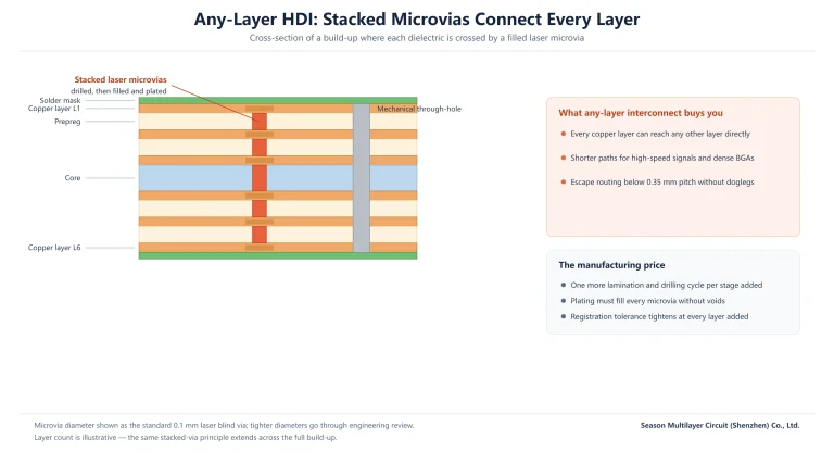
Yes. Laser-drilled blind vias and stacked or staggered microvia structures work on hybrid builds; the sequencing — which stages are drilled and plated before which lamination cycles — is planned at engineering review together with the material pairing. The RF benefit compounds, since microvia fanout shortens the very paths that justify the low-loss material.
What information does a fabricator need to quote a hybrid stackup?
The RF regions and their net classes, impedance targets with tolerances, layer count and thickness, surface finish, any backdrilling, and either a preferred laminate system or the frequency and loss budget so the fabricator can propose one. Volume and thermal environment complete the picture — both change the lamination approach and the material pairing on offer.
Get Your Hybrid Stackup Reviewed Before You Release It
Send your Gerber package, stackup targets and RF net classes through our PCB manufacturing services page, and the engineering review will return a material recommendation with two or three pairing options, the impedance strategy per region, and a firm quotation — before you commit the design. The review also flags lamination and registration risks specific to your layer count, so the first prototype lands where the simulation said it would.