Book Appointment Now

Eight working rules for PCB stackup design, covering layer assignment, reference planes, even layer counts and cost control, with 4-, 6- and 8-layer templates.
PCB Stackup Design: 8 Rules for Signal Integrity and Cost
Last reviewed: October 2026. The rules below reflect current IPC-6012 Class 2 and Class 3 practice.
Most multilayer problems show up late, and most trace back to the same place in PCB stackup design: a board that warps after reflow, a memory interface that fails margin at the edge of tolerance, a power rail that rings every time a motor starts. In a large share of these cases the root decision was made before the first trace was routed — in the PCB stackup design. Layer assignment, reference planes and symmetry determine how much signal-integrity headroom, EMC margin and manufacturing yield a design will have, long before firmware or layout fine-tuning can react.
This article condenses the eight PCB layer stackup rules our engineering team applies when reviewing customer builds, from simple 4-layer boards to 30-layer backplanes. Each rule is stated with the reasoning behind it, the symptom you see when it is broken, and the trade-offs involved. Reference stackups for 4, 6 and 8 layers, a mistake table and a pre-release checklist are included so you can audit your own build before sending Gerber data out for review.
Table of Contents
- Why PCB Stackup Design Comes Before Any Routing
- Rule 1: Assign Layers by Function
- Rule 2: Give Every Signal Layer a Single Reference Plane
- Rule 3: Isolate Power Domains on Multi-Rail Boards
- Rule 4: Keep Ground Planes Multiple and Continuous
- Rules 5 and 6: Routing Combinations and Direction Discipline
- Rule 7: Prefer Even Layer Counts
- Rule 8: Design to a Cost Target
- Reference PCB Stackup Designs for 4, 6 and 8 Layers
- A Pre-Release Stackup Review Checklist
- FAQ
- Get Your Stackup Reviewed Before You Route
Why PCB Stackup Design Comes Before Any Routing
PCB layer stackup rules rest on a simple premise: a stackup is not just a list of layers. It fixes the impedance environment every trace will live in, the return path every switching current will follow, and the mechanical symmetry that decides whether the laminate stays flat through lamination and assembly. Once copper is poured and vias are placed, changing the layer count or moving a plane means re-spinning the layout — one of the most expensive kinds of rework in board development.
The same PCB layer stackup rules also reach into fabrication physics. The number of lamination cycles, the dielectric thicknesses between copper layers and the copper weights all feed directly into yield, warpage behavior and delivery lead time. A stackup that looks elegant in a design tool can be difficult to press or hard to etch symmetrically. The rules below exist because each one protects either an electrical property or a manufacturability property — and the best stackups satisfy both at once.
Rule 1: Assign Layers by Function
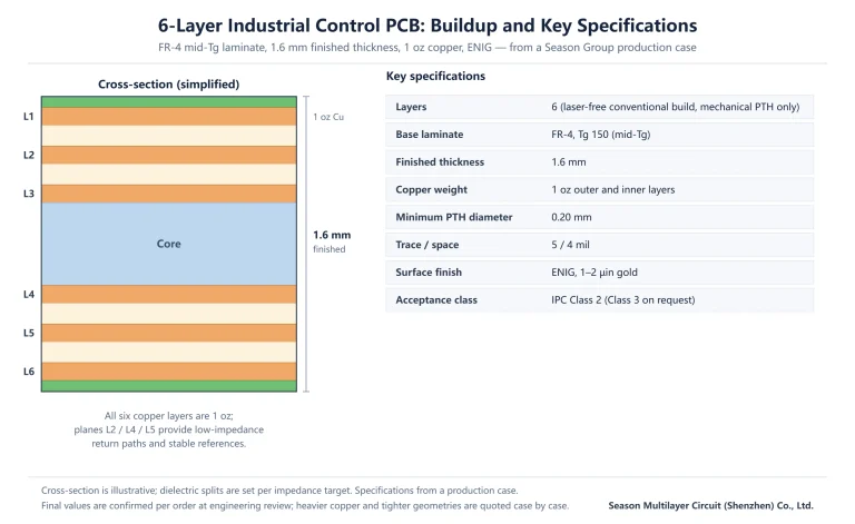
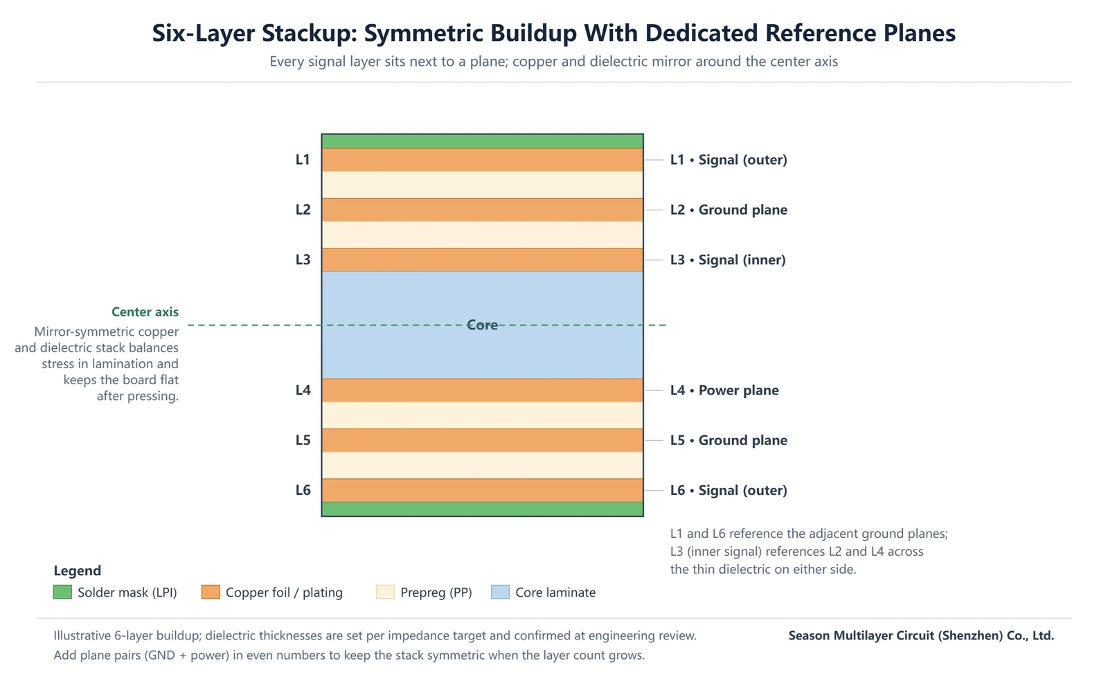
Start by classifying what the board actually carries: high-speed digital signals, sensitive analog signals, power distribution and ground. Every copper layer should be assigned one dominant role — routing layer or plane — and the assignment should follow from those signal classes. A common six-layer arrangement places outer and inner signal layers around dedicated ground and power planes, so that no routing layer is ever far from a low-impedance return path — provided layer-to-layer registration holds the planes where the drawing puts them.
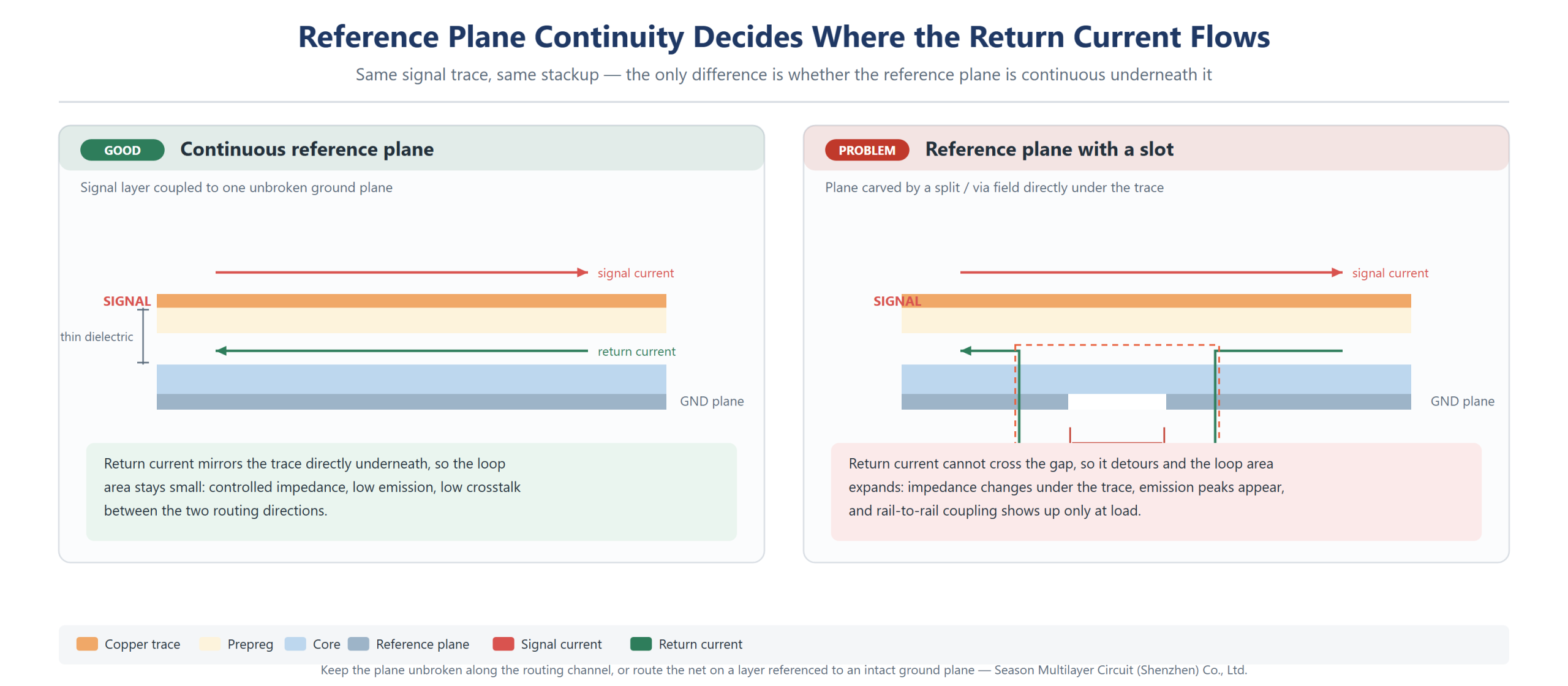
The practical test is simple: for every signal layer, point to its reference plane, and for every power rail, point to its adjacent ground plane. If either answer is missing, the split is not finished. High-speed traces should also avoid crossing plane splits, because the return current cannot follow, and the resulting loop area turns a quiet trace into a radiator. When a net must change layers, a nearby stitching via or return via keeps the loop small.
| Signal or plane type | Typical layer placement | Reason |
|---|---|---|
| High-speed digital (memory, serializer, clock trees) | Outer or inner signal layer directly adjacent to a continuous ground plane | Short, unbroken return path; controlled impedance from the first foot of trace |
| General-purpose digital I/O | Inner signal layer paired with ground or power plane | Shielding from external noise; routing density without crosstalk growth |
| Analog front-end signals | Separate signal layer, or same layer with a guard ground, adjacent to ground | Keeps switching noise out of the analog return path |
| Power rails | Dedicated plane layer or wide polygon, paired with ground | Low power-delivery impedance and contained rail noise |
| Ground | Full plane layer, never fragmented | Reference for impedance and the common return for every switching current |
Rule 2: Give Every Signal Layer a Single Reference Plane
In reference plane PCB design, each signal layer should couple tightly to one adjacent plane — ideally a ground plane. Tight coupling means thin dielectric between the routing layer and its reference, which lowers loop inductance, contains field lines and keeps the impedance of every trace on that layer consistent across the panel — the impedance measurement methods confirm what the stackup actually delivers. When a signal layer faces two different planes at similar distance, return paths become ambiguous and crosstalk between the two routing directions grows.
A quick way to test this PCB stackup design rule on a live layout is to flood-select every trace on a signal layer and ask what its return current does at the far end of the board. If the answer requires jumping across a plane split, the reference is already broken. On a PCB stackup design review we run the same test in reverse: start from the plane, and confirm that every routing channel above it stays inside one continuous copper region. Symmetric dielectric heights on both sides of a plane pair matter here too, because an asymmetric pair tilts the field toward the thinner side and quietly shifts the impedance of everything routed above it.
Decoupling supports this rule at the package and board level. Bulk and local decoupling capacitors belong close to the devices they serve, with short vias into the plane pair, so that transient current is supplied before it propagates across the board. On well-built plane pairs the plane cavity itself carries much of the high-frequency return; capacitors then only need to refill the lower-frequency portion of the current loop.
Rule 3: Isolate Power Domains on Multi-Rail Boards
Boards with several rails — a common case in industrial and communications equipment — should not merge unrelated rails onto one plane island by accident. Make that merge a deliberate decision. Rails with different noise character (a switching regulator output versus a clean analog supply) or different voltage domains should occupy separated plane regions. Each region is paired with its own ground where the return currents allow it. The split boundaries should be straight and crossed by as few signals as possible.
Where a signal must cross a power-plane split, route it on a layer referenced to ground instead, or provide a local stitching structure so the return can detour cleanly. This is one of the least glamorous rules in PCB stackup design and one of the most frequently violated; The symptoms are expensive to debug after the fact: scattered emission peaks, and rail-to-rail coupling that appears only at load.
Rule 4: Keep Ground Planes Multiple and Continuous
In boards of six layers and above, more than one full ground layer is usually the right call in PCB stackup design. Multiple continuous ground planes shorten return loops for inner signal layers, improve shielding between routing layers, and reduce ground impedance at the frequencies where digital noise lives. The planes should be stitched generously with vias along the routing regions so that any layer transition of a high-speed net lands on an immediately available return path.
Continuity matters more than count. A ground plane carved into fragments by dense via fields or long plane splits loses the very properties that justified it. In reference plane PCB design reviews, watch for slots formed by connector fields and BGA anti-pads aligned in rows — see via-in-pad technology for where those anti-pad clusters come from; repositioning a few vias often restores a solid reference without changing the layer count.
Stitching is cheapest at the design stage and most expensive after the fact, so treat via fences as part of the stackup decision rather than a layout detail. A practical target is a ring of ground vias at a spacing that stays well below a quarter wavelength at the highest frequency of interest, placed around every high-speed routing region and along both sides of any plane boundary that a fast net must cross. In reference plane PCB design reviews, the check that catches most escapes is simple: overlay all plane layers and look for any place where two routing channels share a reference that is not continuous beneath both of them.
Rules 5 and 6: Routing Combinations and Direction Discipline
A PCB stackup design should anticipate how layers will be used together. Adjacent routing layers should run in orthogonal preferred directions — horizontal on one layer, vertical on the next — so that overlapping segments are minimized and forward coupling between neighbors stays low. Layer pairs that carry the fastest nets should face a plane on each side, while slower general-purpose nets can share layers further from the planes.
Direction discipline also constrains via usage: every unnecessary layer transition adds a stub, a return-path discontinuity and a drill. Keeping each net on as few layers as practical, and preferring short, direct combinations between adjacent layers, preserves both signal quality and drilling yield. These choices belong in the stackup stage because they determine which layers need plane adjacency in the first place.
One more combination deserves a note: backdrilled and stacked versus staggered microvia builds break the neat pairing of routing layers around a plane, because a removed stub changes which reference a transition actually sees. When a stackup uses sequential lamination, note the via structure per layer pair in the drawing so the fabricator and the layout engineer work from the same picture, and every even layer PCB stackup drawing should carry that note. Where a design mixes very fast differential pairs with slow control signals on adjacent layers, separate them by a ground plane instead of relying on direction discipline alone to keep crosstalk in check.
Rule 7: Prefer Even Layer Counts
An even layer PCB stackup follows from the press itself: laminated boards are pressed as a symmetric sandwich, and even layer counts make that symmetry natural. An odd layer count leaves the copper and dielectric distribution unbalanced, which raises the risk of warpage after lamination and after reflow — a real problem for panels that go through double-sided SMT. Even layer PCB stackup counts also pair more naturally with plane layers, since routing layers tend to come in pairs around a plane.
If a PCB stackup design seems to need an odd count, first check whether a plane can absorb a routing function or whether the extra layer is genuinely required. Where an odd count is justified — some RF and backplane designs — the asymmetry must be compensated in the stackup. Adjust prepreg glass styles and copper distribution so the neutral axis stays near the center. Our balanced stackup and warpage control guide covers that calculation in detail, and our lamination process overview explains how each cycle stresses the stack.
Rule 8: Design to a Cost Target
Every layer added to a board multiplies material, drilling, plating and inspection effort, so the stackup should carry the minimum layer count that meets the electrical requirements — not the maximum that fits the design tool. In relative terms, moving from four to six layers typically raises the board cost by roughly 30–60%, a second lamination cycle on an HDI build adds a further 30–100%, depending on the via structure. Those are ratios, not quotes; actual figures depend on size, copper weights and yield class.
Material choice is the other lever. Standard FR-4 with a mid-Tg resin covers the majority of industrial and communications builds; moving to specialty laminates only pays off when skew, loss or temperature requirements genuinely demand it, as our FR-4 laminate selection guide walks through. Standardizing layer counts, hole sizes and copper weights across a product family also keeps repeat orders on known-good tooling, which shows up later as shorter lead times and steadier quality. Where certification matters, acceptance class and UL recognition of the laminate should be confirmed with the fabricator before the stackup is frozen.
Reference PCB Stackup Designs for 4, 6 and 8 Layers
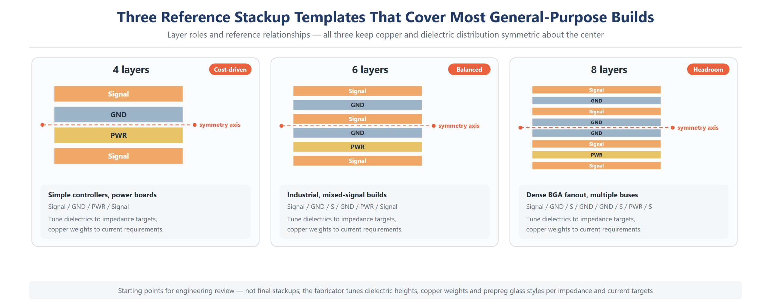
The table below collects three stackup templates that cover most general-purpose builds. They are starting points: dielectric thicknesses are then tuned to the impedance targets, and copper weights to the current requirements, as our heavy copper design rules explain for high-current builds. All three keep the copper and dielectric distribution symmetric about the center, which is what allows a fabricator to press them flat and repeat the result across production lots.
PCB layer stackup rules turn a layer sequence into an impedance plan through two levers: the dielectric height between a trace and its reference, and the trace geometry that sits on top of it. The table below gives starting geometry for the three targets we see most often in review — 50 Ω single-ended and 90 / 100 Ω differential. Treat the values as a first pass that gets a layout close, not as a specification. Final width and spacing are confirmed against an impedance coupon built with the actual laminate, prepreg style and copper weight, which is why we ask for the coupon result alongside the stackup drawing. Every PCB layer stackup rules review we run starts from that assumption.
| Target | Layer pair | Dielectric height H | Trace width W | Gap S (differential) |
|---|---|---|---|---|
| 50 Ω single-ended | Outer microstrip over GND | 0.10–0.12 mm | 0.18–0.20 mm | — |
| 50 Ω single-ended | Inner stripline between GND planes | 0.10 mm per side | 0.10–0.12 mm | — |
| 90 Ω differential | Outer microstrip over GND | 0.10–0.12 mm | 0.15 mm | 0.16–0.20 mm |
| 90 Ω differential | Inner stripline between GND planes | 0.10 mm per side | 0.10 mm | 0.13–0.16 mm |
| 100 Ω differential | Outer microstrip over GND | 0.10–0.12 mm | 0.13 mm | 0.20–0.25 mm |
| 100 Ω differential | Inner stripline between GND planes | 0.10 mm per side | 0.09 mm | 0.17–0.21 mm |
Three cautions apply to every line of that table, and each one is a reference plane PCB design question as much as a fabrication question. First, the numbers assume a soldermask-covered outer layer or an inner layer in FR-4 with a mid-Tg resin; a low-Dk laminate shifts every width upward, and a hybrid build needs the geometry recalculated per layer. Second, an even layer PCB stackup leaves the pair geometry free on every routing layer, and differential spacing controls both the differential impedance and the amount of coupling, so a pair quoted at 100 Ω can be built with wide spacing and loose coupling or narrow spacing and tight coupling — agree which one the design assumes. Third, width tolerance and etch factor move the finished impedance more than most designers expect, which is why the coupon check belongs in the same review as the stackup.
The table below collects three stackup templates that cover most general-purpose builds. They are starting points: dielectric thicknesses are then tuned to the impedance targets, and copper weights to the current requirements, as our
Reading the table needs one caution: the middle two columns describe intent, not copper order on the finished panel. The fabricator translates layer roles into specific cores and prepreg sheets, and a six-layer even layer PCB stackup built from two cores behaves differently under thermal cycling than the same layer count built with a foil-laminated construction. Ask for the material build that will actually be pressed, not only the layer sequence, and check that the reference plane PCB design assumptions in layout match the dielectric heights you are quoting against.
| Layer count | Stackup (top to bottom) | Best suited for | Relative cost trend |
|---|---|---|---|
| 4 layers | Signal / GND / PWR / Signal | Simple controllers, power boards, cost-driven consumer devices | Baseline |
| 6 layers | Signal / GND / Signal / PWR / GND / Signal | Industrial controls, communications modules, mixed analog-digital boards | ≈ +30–60% vs 4 layers |
| 8 layers | Signal / GND / Signal / Signal / GND / PWR / GND / Signal (variants common) | High-speed digital with multiple buses, backplanes, dense BGA fanout | ≈ +60–120% vs 4 layers |
For a worked six-layer example, the diagram at the top of this article shows the layer roles and the reference relationships in cross-section. When the requirement grows past eight layers or into fine-pitch BGA territory, sequential builds with microvias enter the picture; the HDI PCB technology guide explains how 1-Stage, 2-Stage, 3-Stage and Any-layer constructions extend the same symmetric principles, and a produced 8-layer security system PCB shows the stackup applied end to end.
A Pre-Release Stackup Review Checklist
Before a stackup is released to layout under these PCB layer stackup rules — and again before Gerber data is sent out — the following checks catch most of the issues our engineers see in incoming reviews. They take minutes and prevent respins that take weeks.
- Every signal layer names its reference plane, and no routing layer sits between two planes at similar distance without a decision.
- No high-speed net crosses a plane split — the first habit to build in reference plane PCB design; layer transitions of fast nets have an adjacent return via.
- Ground planes are continuous; no connector or via field slots a reference across a routing channel.
- Copper and dielectric distribution is symmetric about the center axis; the neutral axis passes through a core or plane pair.
- Impedance targets are listed per layer class (single-ended and differential), the output of the reference plane PCB design decisions above, with the dielectric heights that achieve them.
- Copper weights, minimum hole size and minimum trace/space are within the fabricator’s stated capability.
- Acceptance class (IPC Class 2 or Class 3 per IPC-6012) is stated so inspection criteria are unambiguous.
- Material designators, glass styles and soldermask/LPI selections are written into the stackup table, not left to verbal agreement.
Sending this checklist with your data is the fastest way to get a PCB stackup design reviewed the fabricator’s engineering questions to a single round. The table below lists the mistakes that survive most often into production, with the symptom each one produces.
| Common mistake | Symptom later in the project | Correction |
|---|---|---|
| Signal layer without an adjacent plane | Impedance varies across the layer; emissions spike at layer transitions | Re-pair the layer with a plane or move the fast nets |
| Fast net crossing a power-plane split | Radiated emission peaks; intermittent margin failures at temperature | Re-route on a ground-referenced layer or add a stitching structure |
| Odd layer count with asymmetric copper | Warp after lamination or reflow; fixture problems in assembly | Rebalance to even count or compensate prepreg/copper distribution |
| Planes fragmented by via fields | Return loops lengthen; crosstalk rises between routing layers | Rework anti-pad rows and add ground stitching |
| Impedance targets missing from the stackup table | Fabricator guesses dielectric heights; first article misses tolerance | State per-class targets and confirm dielectrics at engineering review |
Frequently Asked Questions
What is PCB stackup design and why does it matter?
PCB stackup design is the plan of copper layers, planes and dielectric heights that a multilayer board is built from. It fixes the impedance environment, return paths, EMC behavior and mechanical symmetry before routing starts, which makes it the highest-leverage decision in multilayer design — a stackup change after layout usually means a full re-spin.
What are the core rules of good PCB stackup design?
The working set is: assign layers by function, give every signal layer a single adjacent reference plane, isolate unrelated power domains, keep ground planes multiple and continuous, plan routing combinations and direction per layer pair, prefer even layer counts, and design to a cost target by carrying the minimum layer count that meets the electrical requirement.
Why does an even layer PCB stackup dominate multilayer designs?
Even counts let the copper and dielectric distribution mirror around the center axis, so lamination stress stays balanced and the board stays flat through pressing and reflow. Odd counts leave the sandwich asymmetric and raise warpage risk on double-sided SMT panels; where an odd count is unavoidable, the fabricator must compensate with prepreg and copper distribution.
How do I choose reference planes for high-speed signals?
In reference plane PCB design, the first rule is to reference each high-speed routing layer to one continuous ground plane across thin dielectric. Keep the plane unbroken along the routing channel, add a return via next to every layer transition of a fast net, and avoid crossing plane splits. If a signal must reference power, that rail needs solid decoupling to ground so the return path stays low-impedance.
How many layers does my board actually need?
Let the escape and bus requirements decide, not habit. Four layers serve simple controllers; six layers suit industrial and mixed-signal boards that need shielded inner routing and a power pair; eight and above suit dense BGA fanout and multiple high-speed buses. Adding layers to an even layer PCB stackup multiplies cost roughly 30–60% per step, so carry the minimum count that meets timing, impedance and EMC requirements.
Does a symmetric stackup really prevent warpage?
PCB layer stackup rules treat symmetry as the single biggest lever on flatness. Symmetric copper and dielectric distribution keeps the neutral axis centered so residual lamination stress does not bend the panel. It is not the only factor — copper coverage balance within a layer and assembly profiles matter too — but an asymmetric stackup cannot be fixed by processing adjustments downstream.
What should I send for a stackup review before fabrication?
Send Gerber data with the PCB stackup design table: layer functions, material designators, dielectric heights, copper weights, impedance targets per layer class and the acceptance class. A fabricator’s engineering team can then confirm manufacturability, propose dielectric adjustments and quote lead time in one pass instead of trading questions over several days.
Get Your Stackup Reviewed Before You Route
Season Multilayer Circuit (Shenzhen) Co., Ltd., part of the 998 PCB Group founded in 2006, reviews stackups as part of every quoting cycle. Layer assignment, symmetry, impedance targets and manufacturability are checked in one engineering pass, supported by 3,000,000 m² of annual group capacity across three plants. Send your stackup table and Gerber data through our PCB manufacturing services page for an eight-point review against the rules above, or run the pre-release checklist yourself first and bring us the questions it raises. Either way you get review comments and a production plan rather than a bare price.