Book Appointment Now

What an 8-layer face recognition PCB looks like in production: camera data path, MIPI impedance control, stackup, inspection gates and lead-time windows.
8-Layer Face Recognition PCB: Stackup, Signal Path and Manufacturing
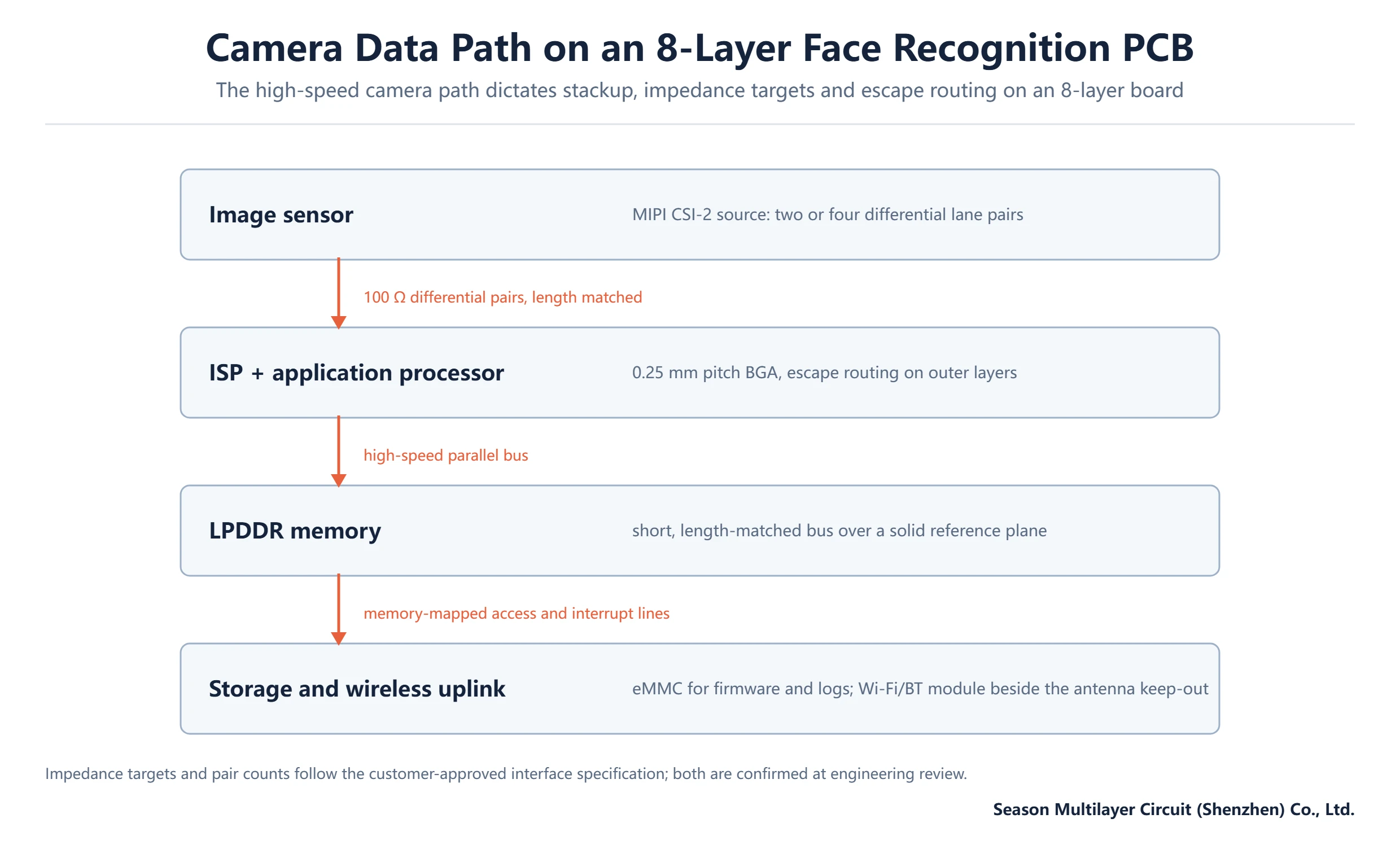
A face recognition terminal lives or dies by its image chain: the sensor feeds raw frames over a camera interface into an image signal processor, the ISP and application processor crunch inference workloads, and the result has to reach memory, storage and the network without dropping a frame. An 8-layer face recognition PCB is the board class where all of that fits with clean signal integrity — enough layers to give every high-speed link its own reference plane, without paying for laser microvias the design may not need. This article breaks down the reference build we fabricate for access-control terminals, AI cameras and smart door locks: the data path, the stackup, the impedance and routing rules that matter, and what inspection and lead time look like in production.
It is written for hardware engineers and sourcing teams evaluating fabricators, from the manufacturer side. Where a value depends on your sensor choice or module selection, we flag the engineering review that settles it. For the generic layer-count logic behind this board class, our multilayer PCB overview is the shorter read.
Table of Contents
- What Is an 8-Layer Face Recognition PCB
- Reference Build Specification
- Camera Data Path and Impedance Control
- The 8-Layer Face Recognition PCB Stackup, Layer by Layer
- BGA Escapes and Memory Routing
- Inspection Gates and Reliability Verification
- Prototype and Volume Lead Times
- Cost Structure in Relative Terms
- Review Your Vision Board Before You Release Gerber Data
- FAQ
- Request an Engineering Review for Your Vision Terminal
What Is an 8-Layer Face Recognition PCB
An 8-layer face recognition PCB is the main board of a vision device: it carries the image sensor interface, the ISP and application processor with its memory, storage, power management and usually a wireless module for enrollment and cloud sync. Eight layers is the point where the camera interface, the memory bus and the power section each get dedicated routing resources instead of competing for the same two signal layers.
The build class covers a wide family of devices — access-control panels beside doors, wall-mounted attendance terminals, smart door locks with a viewer, and fixed AI cameras for retail analytics. What they share is a high-speed serial camera link and a processor dense enough for on-device inference, which together set the electrical requirements that a plain four-layer board struggles to meet. Where the device is part of a larger security system, the board often sits next to an 8-layer security system PCB in the same enclosure family, sharing the same manufacturing recipe.
The reference specification below is a real repeating build, not a theoretical example. Treat it as a conversation starter for engineering review.
Reference Build Specification
The reference build for an 8-layer face recognition PCB centers on a 1.6 mm symmetric board on a Tg 170 FR-4 grade, with mechanically drilled through-vias only. It is deliberately a standard multilayer build: unless your sensor module forces a different connector field, through-via technology carries this design class comfortably, which keeps cost and lead time at mainstream levels.
| Parameter | Reference build |
|---|---|
| Layer count | 8 layers, symmetric buildup |
| Base laminate | FR-4 grade, Tg 170 |
| Finished board thickness | 1.6 mm |
| Production panel | 145 × 119 mm, single board per panel |
| Outer copper | 35 µm (1 oz) |
| Inner copper | 30 µm (≈0.85 oz) |
| Minimum drilled hole | 0.20 mm plated through-hole |
| Minimum trace and space | 3/3 mil (0.076/0.076 mm) |
| Surface finish | ENIG |
The single-up 145 × 119 mm panel reflects the geometry of a wall-mounted terminal — taller than wide, with the camera window and IR illuminator cutouts fixed by the mechanical housing. When device volume grows, the review re-panels the same circuit onto a multi-up production panel, which is one of the quiet cost levers explained later in this article.
Camera Data Path and Impedance Control
The camera link dominates the electrical design. A typical sensor connects over MIPI CSI-2 using two or four differential lane pairs, each pair a tightly coupled, length-matched 100 Ω differential run from the sensor connector to the ISP or processor. These pairs want the shortest practical path, an uninterrupted reference plane beneath them, and spacing from any single-ended switching noise — which is exactly what the ground planes in the stackup section provide.
Downstream, the ISP and application processor talk to LPDDR memory over a short parallel bus, to storage over its own interface, and to the wireless module for enrollment events and firmware updates. Each link has its own impedance and length-matching targets, all confirmed from your interface specification during review rather than assumed. The discipline that keeps this path healthy in production is unglamorous: pair routing without stubs, return paths that never cross a plane split, and crystal plus regulator placement that keeps their spectral energy away from the camera connector.
If your design uses dual sensors or an added structured-light projector, the lane count doubles but the rules do not change — the stackup simply carries more pairs on the same layers. We verify every target with TDR measurement on a test coupon that travels with each production lot.
The 8-Layer Face Recognition PCB Stackup, Layer by Layer
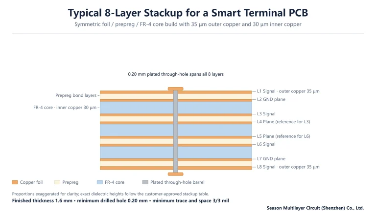
The stackup is symmetric: copper foil on both outer surfaces, prepreg bonding layers, and three FR-4 cores. The electrical assignment runs L1 signal, L2 ground, L3 signal, L4 plane, L5 plane, L6 signal, L7 ground, L8 signal from top to bottom. Every signal layer references an adjacent plane — L1 pairs against L2 for the camera interface, L3 against L4, L6 against L5, L8 against L7.
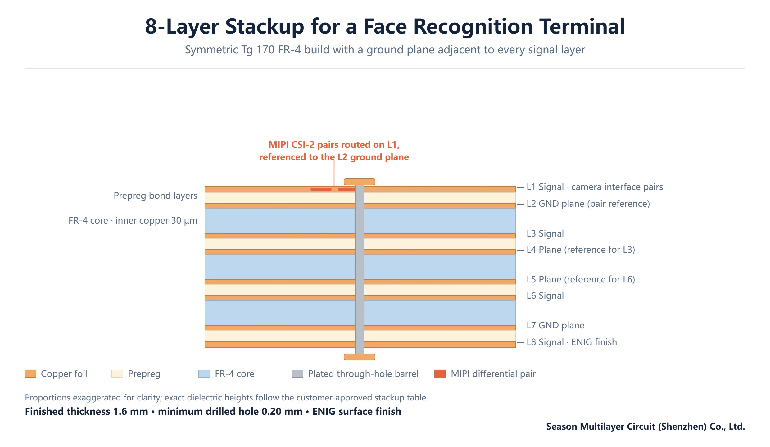
Outer copper is 35 µm (1 oz) for connector fanout and power entry, inner layers 30 µm. The 0.20 mm minimum drilled hole is a mechanically drilled plated through-hole spanning all eight layers — no lamination cycles beyond the standard sequence, which is why this build class prototypes quickly. If your processor needs finer escape than 3/3 mil provides, the review prices the move to HDI laser microvia technology against its added cycles before you commit the layout.
Symmetry also carries the mechanical story: a wall-mounted terminal bolts into a housing at fixed standoffs, and a balanced board stays flat through reflow and over temperature. Any stackup change on one side of the centerline is mirrored on the other as part of the same review.
BGA Escapes and Memory Routing
Vision-class processors commonly sit at 0.25 mm ball pitch. At that pitch a through-via fits between four balls, and escape routing proceeds on the layer directly under the device — L1 for the first channel, L3 for the second after the ground plane. With 3/3 mil trace and space, each ball row escapes reliably without via-in-pad filling, keeping the build in standard multilayer territory.
- Escape the first two BGA rows on L1, break to L3 through short vias placed between ball columns.
- Keep LPDDR address and data runs short and length-matched over the adjacent ground plane.
- Route camera pairs first, then memory, then everything else — the order protects the links with the tightest budgets.
- Place decoupling where the balls are, not where the layout tool finds room.
Memory is usually the forgiving part of the design; the camera interface is not. That is why the routing order above puts the MIPI pairs down first, while tolerance still exists on every layer, and why we ask for your sensor module datasheet early in review — the connector pinout decides whether the pairs enter the board from the left edge or the top, and that decision cascades through the whole layout.
Inspection Gates and Reliability Verification
The inspection plan for this build class puts automated optical inspection on every copper layer before lamination, then 100% electrical test — flying probe or fixture, by volume — on finished boards. First-article cross-sections verify hole copper and layer registration inside the finished thickness, and TDR impedance coupons confirm the 100 Ω camera pairs and memory bus targets on the shipped build.
| Gate | Method | Why it matters for vision boards |
|---|---|---|
| Inner-layer artwork | AOI before lamination | Fine camera-pair routing is checked before it is buried |
| Layer registration | First-article cross-section | Pairs stay coupled to their reference plane where designed |
| Netlist integrity | 100% flying probe or ICT | Every net matches Gerber data before assembly |
| Impedance | TDR test coupon per lot | Camera pairs ship at 100 Ω, not at nominal guesswork |
| Finish quality | Visual and thickness check | ENIG solderability survives multiple assembly passes |
On top of the standard gates, terminal products often add customer-specified checks — insulation resistance and voltage withstand on the power section, or extended visual criteria on the camera window area where the housing is transparent. Acceptance criteria reference the IPC standards for rigid board workmanship, and any device-specific additions are agreed in review and archived with the build record.
Prototype and Volume Lead Times
Prototypes for this build class typically complete in 5–7 working days once engineering review is closed; volume runs land in the 15–20 working day range depending on quantity and panel loading. Both windows assume a confirmed stackup and no special-material allocation — the binding schedule for your order is set at engineering review.
Volume consistency rests on the same mechanism as any repeatable multilayer product: archived working files, the same panel program and the same inspection criteria reused on every repeat order, with first-article confirmation on each new lot. Production capacity comes from the 998 PCB Group network — three plants in Shenzhen, Jiangxi and Anhui, founded in 2006, running 3,000,000 m² per year across 2–30 layer builds — so seasonal demand peaks do not force a build-recipe change mid-program.
Cost Structure in Relative Terms
Quotation for an 8-layer face recognition PCB responds to the same levers as any multilayer build, expressed here as relative effects rather than prices. Geometry leads: layer count, outline and thickness set the material baseline. Process floor follows: minimum trace and space, minimum hole and via count. Then the quiet levers — surface finish choice and panelization efficiency — often move unit cost more than any single technical parameter.
Panelization is worth dwelling on for vision terminals. The reference 145 × 119 mm single-up panel exists because the housing fixes the outline early; once the mechanical design stabilizes, re-paneling the same circuit two-up or four-up on a 242 × 170 mm panel typically improves material utilization enough to matter at volume, at zero electrical cost. Review optimizes this once, and repeat orders keep the gain. For orientation on the lower end of the market, the two-layer versus four-layer comparison shows how the same levers behave on simpler builds.
Review Your Vision Board Before You Release Gerber Data
If the reference build is close to your design, send your stackup intention, sensor module datasheet and Gerber data for engineering review — we return feasibility comments on camera-pair routing, BGA escape and panel efficiency, together with the production detail for the exact 8-layer security system PCB platform behind this article. If your design needs finer pitch or laser microvias, the review prices that delta before you commit the layout, not after.
Frequently Asked Questions
What files should I provide to quote an 8-layer face recognition PCB?
Gerber data with drill files, your stackup intention, and the sensor module datasheet or at least its connector pinout. Impedance targets for the camera pairs (typically 100 Ω differential) and memory bus length-matching rules help the review return accurate, actionable feedback on the first pass.
How long does a face recognition PCB prototype take?
For a standard through-via build like this reference, prototype fabrication typically completes in 5–7 working days after engineering review closes. Designs that add laser microvias or special laminates take longer due to extra lamination cycles. Your binding schedule is confirmed at engineering review.
Do camera interface pairs really need 100 Ohm differential control?
MIPI CSI-2 lanes are specified around a 100 Ω differential environment, and keeping that target from connector to processor prevents eye-closure artifacts that look like software bugs. We verify the target with TDR measurement on a coupon that ships with each production lot, so the check is a gate rather than an assumption.
Why choose 8 layers instead of 6 for a vision terminal?
Six layers carry one high-speed bus plus a ground plane well. When the camera interface, LPDDR memory bus and wireless module coexist, the extra pair of layers in an 8-layer face recognition PCB gives every signal layer its own uninterrupted reference, which reduces interference between the image chain and the radio.
Which surface finish works best for a camera terminal board?
ENIG is the default here: it stays flat and solderable through repeated assembly passes, which matters when fine-pitch parts sit on both sides and the board reflows more than once. OSP or HASL can suit simpler assemblies; the finish is confirmed during review against your assembly process.
Can the board handle dual cameras or a structured-light projector?
Yes — the lane count doubles but the stackup rules stay the same, with more differential pairs carried on L1 and L3 over their adjacent planes. The review sizes the routing channels against your actual lane count and adjusts the stackup only if the escape density demands it.
How is consistency between prototype and volume production maintained?
Repeat orders reuse the same archived working files, panel program and inspection criteria as the confirmed first article. Each production lot passes 100% electrical test, and TDR impedance coupons travel with every batch, so any drift in the press cycle is caught before boards ship.
Request an Engineering Review for Your Vision Terminal
Send your Gerber data and stackup intention, and our engineering team returns layout-level feedback on camera-pair routing, BGA escape and panel efficiency — typically the same working day. Quotation follows the review, itemized and without hidden line items.