Book Appointment Now

The six bottlenecks that set multilayer PCB fabrication yield above 8 layers, with the countermeasures and design choices that keep first builds on plan.
Multilayer PCB Fabrication: The Six Bottlenecks That Set Yield
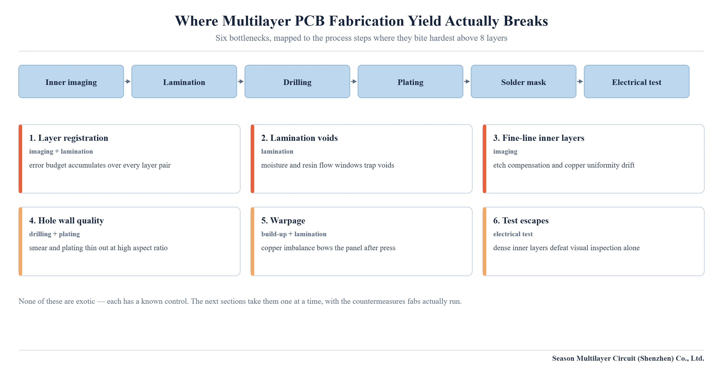
Multilayer PCB fabrication does not get harder in a straight line. Moving from a 6-layer build to a 12-layer build does not double the difficulty — it multiplies it, because every added layer pair adds another registration step, another lamination cycle, and another place where a small error from an earlier process compounds into scrap. Buyers usually discover this through the quote: two boards with similar dimensions, dramatically different prices and lead times.
This article walks through the six bottlenecks that actually set yield above eight layers, what causes each one, and the countermeasures a capable fab runs against them. It is written from the buyer’s side of multilayer PCB fabrication: the goal is not to teach you manufacturing, but to help you judge quotes, ask the right engineering questions, and design the stackup so the hard problems never start.
Table of Contents
- Why Multilayer PCB Fabrication Gets Harder Nonlinearly
- Bottleneck 1: Layer-to-Layer Registration
- Bottleneck 2: Lamination Voids and Delamination
- Bottleneck 3: Fine-Line Inner Layers
- Bottleneck 4: Hole Wall Quality at Higher Aspect Ratios
- Bottleneck 5: Warpage and Thickness Tolerance
- Bottleneck 6: Test Escapes on Dense Inner Layers
- Designing for Multilayer PCB Fabrication Yield
- FAQ
- Have Your Stackup Reviewed Before It Goes to Press
Why Multilayer PCB Fabrication Gets Harder Nonlinearly
Every inner layer is manufactured sight-unseen. Once a core is laminated into the stack, its traces can only be inspected indirectly — which means the processes that build inner layers have to be right the first time, at a precision that compounds across the whole stack. A 4-layer build gives the process two inner images and one lamination cycle to survive; an 18-layer build gives it sixteen images and multiple press cycles, each one a chance for the accumulated tolerance to show up as a misregistered via or an open circuit at electrical test.
| Capability | Volume production | Where it starts to bite |
|---|---|---|
| Layer count | 2–30 layers | Beyond 30: engineering review, prototype-oriented builds |
| Minimum line width / spacing | 2/2 mil | Below 2 mil: yield drops sharply without LDI imaging |
| Through-hole aspect ratio | Up to 12:1 | Higher ratios: plating uniformity and hole-wall risk |
| Blind via aspect ratio | 1:1 | Deeper blind vias move into laser-drilled HDI territory |
Those numbers describe the practical envelope — a multilayer PCB designed comfortably inside it will run at good yield on any competent line. The six bottlenecks below are the places where designs push against the envelope, and where the difference between a mediocre fab and a good one shows up in your scrap rate.
Bottleneck 1: Layer-to-Layer Registration
Registration is the defining difficulty of the process. Each copper layer is imaged, etched and stacked with every other layer, and a via that misses its pad on layer 14 is an electrical open that no amount of outer-layer inspection will reveal. The error budget has four contributors: material dimensional change as cores and prepreg absorb moisture and heat, artwork scaling error when film is plotted without compensating for production growth, tooling and punch drift over a tool’s life, and resin flow that physically drags inner layers during the press cycle.
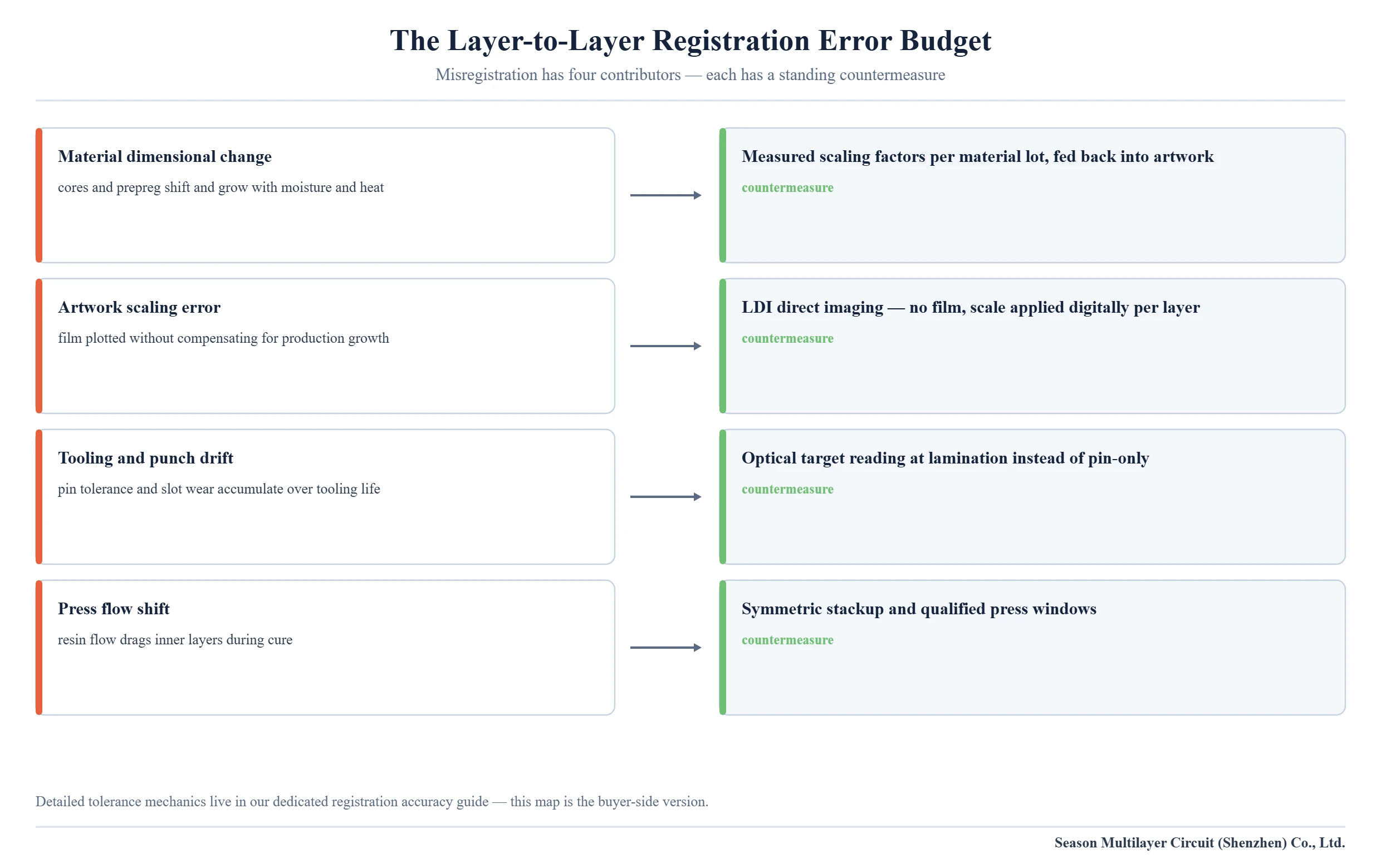
- Measured scaling factors per material lot, fed back into the artwork instead of assumed from a datasheet
- LDI direct imaging, which removes film entirely and applies scale digitally per layer
- Optical target reading at lamination rather than pin-only alignment
- Symmetric stackup construction so press stresses cancel instead of shifting layers
The tolerance mechanics — how these errors add up across a stack — are covered in depth in our layer-to-layer registration accuracy guide. The buyer-side takeaway: registration capability is set by measurement discipline, not by machine brochures, and it is the first thing to ask about when a quote for 12+ layers looks suspiciously cheap.
Bottleneck 2: Lamination Voids and Delamination
The press cycle is where separate cores become one board, and it is unforgiving of preparation mistakes. Moisture absorbed by prepreg before lamination turns to vapor under heat and pressure and forms voids between layers. Resin that has flowed too far starves the dielectric; resin that has not flowed enough leaves bonding gaps that show up later as delamination during assembly reflow or thermal cycling.
The controls are procedural rather than exotic: vacuum-assisted lamination to pull entrapped air out before the resin gels, bake cycles timed to the prepreg’s actual moisture content rather than the calendar, and press windows — temperature ramp, pressure steps and dwell — qualified per material system rather than shared across all of them. The press cycle itself is explained step by step in our PCB lamination process guide.
For buyers, the practical check is design-side: keep copper balanced through the stack and avoid huge resin-poor regions, because a stackup with large bare areas on one face and heavy copper on the other is asking the press to solve a physics problem it cannot. The stackup rules in our stackup design guide exist largely for this reason.
Bottleneck 3: Fine-Line Inner Layers
Inner layers carry the densest routing on the board and get the least forgiveness. Etch tends to undercut traces, so the artwork is compensated — drawn slightly wider so the finished trace lands on target — and the compensation value depends on copper thickness, line width and etch chemistry. Get it wrong and traces drift narrow across the panel, with the thinnest ones failing continuity or, worse, passing test with marginal copper that ages poorly.
Copper thickness uniformity across the panel is the quiet variable here: plating that runs thick in one corner changes the etch behaviour there, and the compensation that was correct in the center is wrong at the edge. This is why volume production holds 2/2 mil line width and spacing as the comfortable floor while sample builds can push to 1.8/1.8 mil, and why fabs that run LDI exposure and controlled-chemistry etch hold fine-line yield far better than those still plotting film. The inner-layer process from dry film to etch is detailed in our inner layer fabrication guide.
Bottleneck 4: Hole Wall Quality at Higher Aspect Ratios
Every via in a multilayer board has to be drilled through stacked, cured laminates and then plated reliably down a hole wall that gets longer as boards get thicker. Two failure mechanisms dominate. Drill smear — resin melted by the drill bit coating the hole wall — insulates the copper layers from the plating chemistry and produces barrel voids. And at higher aspect ratios, plating current distributes unevenly, depositing thick at the mouths and thin at the middle of the hole.
This is why through-hole aspect ratio is held to 12:1 in routine production: below that, desmear chemistry and plating agitation keep the hole wall intact with wide margins; above it, every parameter tightens and scrap risk climbs. Hole formation — mechanical versus laser drilling, entry and backup materials, hit counts — is covered in our PCB drilling process guide. For the designer, the cheapest fix is again envelope-respect: keep via aspect ratios inside the table in the first section and let the fab spend its attention on the layers that genuinely need it.
Bottleneck 5: Warpage and Thickness Tolerance
A multilayer stack is a laminate of materials with different expansion behaviour, and copper is the one that dominates the outcome. Copper pulls against the resin system as the board cools after press; when the copper distribution is asymmetric, the panel cools into a bow. The acceptance reference is IPC-6012: bow and twist capped at 0.75% for Class 2 and 0.5% for Class 3. A panel that ships flat passes; a panel that ships at 1% warps on the SMT conveyor and turns into an assembly yield problem you will pay for twice.
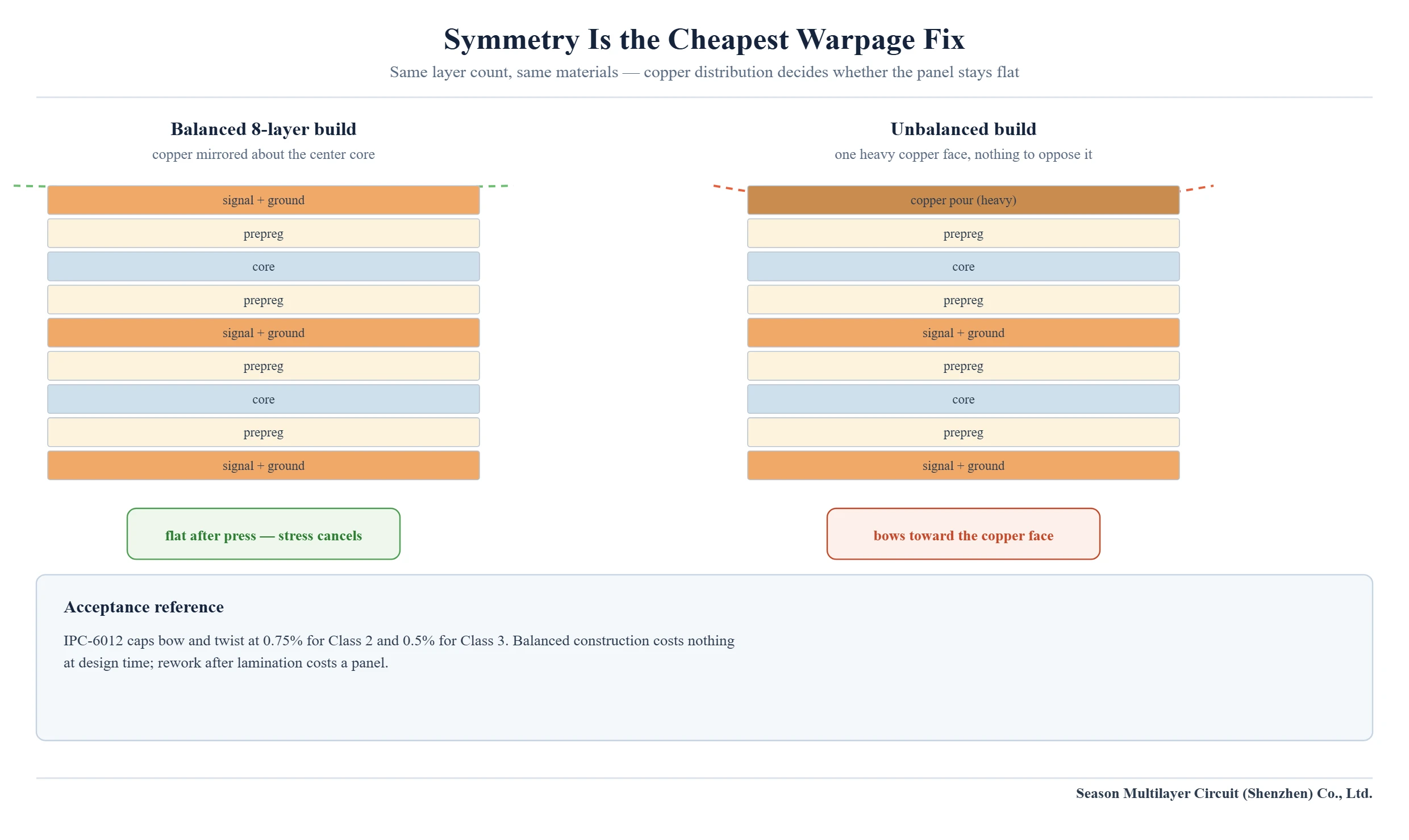
Symmetry is the cheapest warpage fix available — mirroring copper about the center core costs nothing at design time, while correcting a bowed panel after lamination costs the panel. The full mechanics, including how dielectric thickness choices interact, are in our balanced stackup and warpage control guide.
Bottleneck 6: Test Escapes on Dense Inner Layers
The last bottleneck in multilayer PCB fabrication is the one that lets the first five through. Inner layers cannot be visually inspected once laminated, so the inspection burden shifts to automated optical inspection before press and electrical test after — and both have coverage limits. AOI catches cosmetic and geometric defects reliably but cannot prove a via connects the right layers. Electrical test proves connectivity but only at nets the test fixture addresses.
Dense designs close the gap with dedicated test hardware: impedance coupons processed on the same panel as the production boards, so the stackup’s actual impedance is measured, not inferred; and netlist-based electrical test that compares every net against the design data rather than a fixed fixture. For controlled-impedance builds, our impedance measurement guide explains what the coupon actually verifies, and the reliability testing guide covers the qualification tests that catch the marginal boards AOI and electrical test alone would ship.
Designing for Multilayer PCB Fabrication Yield
Every bottleneck above has a design-side lever, and none of them cost performance. The table below is the checklist we would hand to a hardware team before a 10+ layer multilayer PCB fabrication build goes to RFQ — it is the difference between a stackup that qualifies in one pass and one that eats two prototype rounds.
| Design lever | Bottleneck it protects | Practical guidance |
|---|---|---|
| Symmetric copper distribution | Warpage, registration | Mirror copper about the center core; avoid one-sided pours |
| Respect 12:1 through-hole aspect ratio | Hole wall quality | Prefer smaller drilled diameter over thicker boards where possible |
| Stay above 2/2 mil on inner layers | Fine-line yield | Push below 2 mil only on layers that genuinely need it |
| Order impedance coupons with production | Test escapes | Same-panel coupons; specify tolerance ±10% unless tighter is justified |
| Declare special processes at RFQ | All of them | Undeclared requirements are discovered after drilling, at your cost |
The acceptance criteria behind the first three rows are set by IPC performance standards — IPC-6012 for the board, IPC-A-600 for visual acceptance — and a fab that quotes comfortably inside them is telling you something useful. Bring the same discipline to your data package: clean, self-consistent Gerber data with a readable stackup table removes the interpretation errors that turn good designs into scrap.
When the build is dense enough that these levers stop being enough — fine-pitch BGA fanout, stacked microvias, backplane-class layer counts — the right move is an engineering review before quoting, which is exactly how our 14-layer 2-stage HDI prototype and 10-layer USSD PCB builds are run, and how the manufacturing capability page frames the layer and process envelope.
Frequently Asked Questions
Why is multilayer PCB fabrication harder than double-sided?
Inner layers are processed before lamination and cannot be inspected afterwards, so every inner image, etch and press cycle must land right the first time. Difficulty also compounds: each added layer pair multiplies registration steps and lamination cycles where errors accumulate.
How many layers can be manufactured routinely?
Our production envelope is 2–30 layers in volume, with prototype builds beyond 30 handled case by case under engineering review. Yields are strongest when the design sits inside the capability table rather than at its edges.
How do fabs keep multilayer layers aligned?
Through measured artwork scaling per material lot, LDI direct imaging, optical target reading at lamination, and symmetric stackup construction. Registration is a measurement discipline — the details are in our layer-to-layer registration guide.
What causes voids between PCB layers?
Mostly moisture in the prepreg turning to vapor under press heat, plus resin flow outside its qualified window. Vacuum lamination, moisture-controlled bake cycles and per-material press windows are the standing controls.
What through-hole aspect ratio is safe?
Up to 12:1 is routine in volume production. Beyond that, plating becomes uneven down the hole wall and scrap risk rises, which is why higher ratios are quoted case by case rather than promised by default.
How much bow and twist is acceptable on a PCB?
IPC-6012 caps bow and twist at 0.75% for Class 2 and 0.5% for Class 3. Symmetric copper distribution is the cheapest way to stay inside the limit, since it costs nothing at design time.
How is a multilayer board tested before shipment?
AOI on every layer before press, impedance coupons processed with the production panel, and netlist-based electrical test after. The combination catches what visual inspection alone cannot, especially on inner layers.
What can a designer do to improve multilayer yield?
Balance copper through the stack, keep aspect ratios inside 12:1, hold inner-layer geometry above 2/2 mil where possible, order impedance coupons with the production panel, and declare every special process at RFQ.
Have Your Stackup Reviewed Before It Goes to Press
If your next build crosses eight layers — or you are comparing quotes that disagree by more than the stackup justifies — send us the Gerber package and the stackup table. Engineering review will map the design against the capability envelope, flag the bottlenecks it will hit, and confirm process and lead time before anything is committed. The PCB manufacturing services page lists what a complete RFQ package includes.
For builds that sit comfortably inside the envelope, we will say that too — the goal of the review is a first-pass prototype, not a bigger quote.
Tel: (+86) 18681528532 (WhatsApp)
E-mail: roc@season-pcb.com