Book Appointment Now

How copper filled vias are plated from the bottom up, which parameters control fill quality, and when copper fill beats resin plugging on cost.
Copper Filled Vias: Via Filling Plating Process and Design Rules
A drilled and plated via is a hollow tube. A via that has to carry real current, spread heat, or sit directly beneath a component pad needs to be a solid column of copper, and that is exactly what via filling plating produces. On HDI builds, copper filled vias pass signals between layers with lower resistance and a far better thermal path than a conventional plated barrel can offer. This guide walks through how the fill is actually grown inside the barrel, which chemistry and pulse parameters decide the result, how fill quality is inspected, and when the extra cost is worth specifying.
What follows reflects how production lines run the process, not just how it appears in a textbook. Where numbers matter, they are acceptance windows and capability values confirmed at engineering review before a build is released to the floor.
Table of Contents
- What Via Filling Plating Actually Does to a Via
- Bottom-Up Copper Growth: The Filling Mechanism
- The Three-Additive Chemistry Behind a Void-Free Fill
- Copper Filled Vias vs Resin-Plugged and Tented Vias
- The Process Window That Decides Fill Quality
- Inspection and Acceptance Criteria for Copper Filled Vias
- Design Rules That Keep Filled Vias Manufacturable
- Applications Where Copper Fill Pays Off
- Cost and Lead-Time Impact of Via Filling
- Common Failure Modes and How to Prevent Them
- FAQ
- Get Your Via-Fill Stackup Reviewed Before You Commit
What Via Filling Plating Actually Does to a Via
A conventional via is made by drilling, cleaning the hole wall, depositing a thin electroless copper layer, and then electroplating the barrel. The result is a copper tube roughly 20–25 µm thick with empty space down the middle. For a signal passing through one layer pair, that tube is perfectly adequate. For a via that must be stacked on, mounted over, or asked to conduct meaningful current, the hollow center becomes the weak point.
Via filling plating continues the deposition until the barrel is completely full, turning the tube into a solid copper column. The change is not cosmetic. Electrically, the cross-sectional area of conductor multiplies, so via resistance drops sharply and current capacity rises. Thermally, solid copper conducts heat from one layer to another at roughly 400 W/(m·K), turning every filled via into a small heat channel. Mechanically, a filled barrel supports the layers above and below it when another via is stacked on top.
This is why the technique sits at the core of modern HDI PCB technology. Stacked microvia structures are only as reliable as the fill inside them, and the fill process itself is what decides whether a stack survives assembly and field use.
Bottom-Up Copper Growth: The Filling Mechanism
The defining feature of a correct fill is the direction of growth. In ordinary plating, current density concentrates at the corners of the via mouth, so copper deposits fastest exactly where the barrel opens. If a fab simply extends a normal plating cycle, the mouth closes first and seals a void inside the barrel — the classic defect that via filling plating exists to eliminate.
Filling chemistry inverts that behavior with organic additives working against each other. A suppressor adsorbs at the via mouth and slows deposition there, while an accelerator concentrates at the base and speeds deposition where copper is needed most. The barrel therefore fills from the bottom up, as the diagram below shows, until the growing column meets the surface.
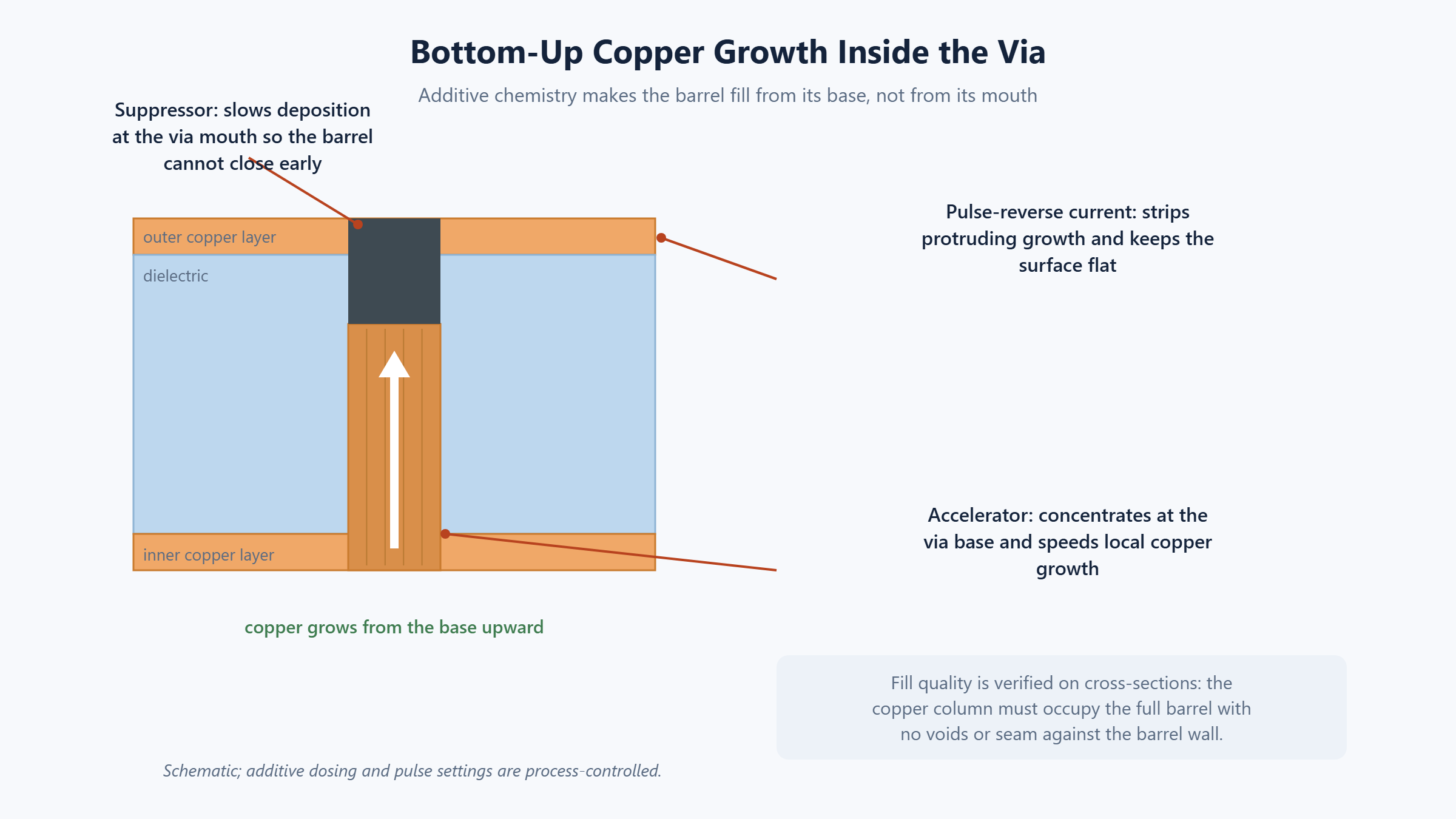
Pulse reverse current completes the picture. By periodically reversing the current for a few milliseconds, the line strips off protruding growth and keeps the surface flat while the barrel below continues to fill. The outcome is a full barrel with no seam, no dimple beyond the specified limit, and a surface that can be plated over cleanly.
The Three-Additive Chemistry Behind a Void-Free Fill
Three families of organic additives share the bath, and each has a precise job. Accelerators, typically sulfur-bearing compounds, concentrate at the via base and catalyze copper deposition where the fill must grow fastest. Suppressors, large polymer carriers, blanket the surface and the via mouth, throttling deposition exactly where nature would otherwise plate too fast. Levelers smooth the growing surface, preventing the bumps and nodules that a pure bottom-up process would otherwise leave behind.
Bath discipline matters as much as the additives themselves. Concentrations drift as plating proceeds, so production lines monitor and dose the bath continuously rather than in batch corrections. Temperature is held in a narrow band, and solution movement through the via field is actively managed — a stagnant bath starves the base of accelerator and the void rate climbs immediately.
Process qualification follows the performance specifications published by the Global Electronics Association, which define how plating processes and finished boards are tested. A fill chemistry that cannot hold its window across a full panel is not production-ready, regardless of how well a coupon performs.
Copper Filled Vias vs Resin-Plugged and Tented Vias
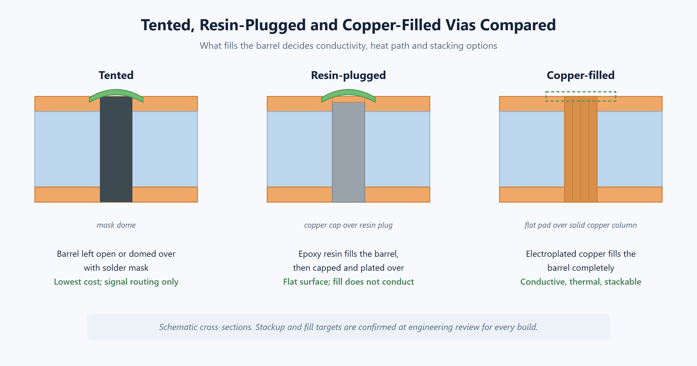
Three treatments compete for the same via, and choosing correctly is a cost decision as much as an engineering one. The table below compares them on the attributes that actually drive a specification.
| Attribute | Tented | Resin-plugged | Copper filled |
|---|---|---|---|
| Fill material | None — mask dome over the opening | Epoxy resin, capped and plated over | Electroplated copper column |
| Electrical conduction through via | Plated wall only | Wall only; fill does not conduct | Wall plus solid fill |
| Thermal path between layers | Poor | Poor to modest | Excellent |
| Component mounted over the via | Not practical | Yes, with cap plating | Yes, flat and conductive |
| Stacked via support | Not suitable | Limited | Designed for it |
| Relative cost impact | Lowest | Moderate | Highest |
| Typical use | Simple signal routing | Under pads on cost-sensitive builds | Stacked HDI, high current, heat spreading |
The practical rule: if the via must conduct, conduct heat, or carry another via on top, copper fill is the only option that does all three. If the via just needs to disappear under a pad on a cost-driven board, a resin plug with cap plating does the job for less, keeping copper filled vias for the structures that genuinely need the conduction. Tenting remains correct for the vast majority of ordinary signal vias — filling everything is wasted money.
The Process Window That Decides Fill Quality
Fill quality is decided by a chain of steps, and a weak link anywhere in the chain shows up as a void on the cross-section. The window below is representative of production practice; the exact settings for a given build are confirmed at engineering review.
| Process step | What is controlled | Target |
|---|---|---|
| Laser drilling | Via diameter and taper | 0.1 mm standard microvia, clean barrel wall |
| Desmear / plasma clean | Residue removal from the hole | Adhesion-ready wall, no smear |
| Electroless copper | Seed coverage on the wall | Continuous conductive layer |
| Fill plating | Pulse waveform and additive dosing | ≥95% fill with no voids or seam |
| Surface copper control | Current distribution across the panel | Flat plating over the fill, no bumps |
Aspect ratio is the governing constraint. Filling is dependable for blind vias up to roughly a 1:1 aspect ratio, which matches the laser microvia geometry used on standard HDI builds. As barrels get deeper and narrower, the accelerator has to fight harder to reach the base, and void risk rises steeply — which is why a stackup with sensible via geometry is cheaper than a heroic fill process.
Inspection and Acceptance Criteria for Copper Filled Vias
Fill quality cannot be judged from the outside. The primary verification is cross-section sampling: production panels are sectioned, polished, and measured for how completely the barrel is filled. Acceptance follows the criteria in IPC-6012 and IPC-A-600 acceptance requirements, which define fill percentage, void limits, and the surface conditions that separate a conforming fill from a reject.
| Acceptance item | Typical requirement | How it is checked |
|---|---|---|
| Barrel fill | ≥95% of the barrel occupied by copper | Cross-section sampling |
| Internal voids | None permitted within the fill | Cross-section, supported by X-ray where specified |
| Dimple over the fill | Within the depth limit in the spec | Cross-section measurement |
| Plating over the fill | Continuous cap, no separation | Cross-section |
| Surface copper thickness | Uniform across the panel | Thickness measurement |
The dimple limit deserves emphasis for anyone stacking vias. If the surface over a fill sinks beyond specification, the via stacked on top of it inherits a registration and reliability problem. A fab that measures dimples on every fill lot, rather than occasionally, is the one you want building stacked structures.
Design Rules That Keep Filled Vias Manufacturable
Most fill problems can be designed out before a quote is ever requested. The rules below cover the decisions that matter most.
- Keep blind microvia diameters in the proven window — 0.1 mm is the standard laser via; going smaller needs a capability review before commitment.
- Respect the aspect ratio: a 1:1 blind via fills reliably; deeper barrels raise void risk and cost together.
- Specify fill only where the function requires it — stacked vias, current-carrying paths, or heat-spreading positions.
- Provide a complete stackup drawing that marks which layers carry filled vias and whether the structure is stacked or staggered.
- State the surface finish over filled pads, since flatness and solderability interact with the cap plating.
- Flag impedance-controlled layers that interact with filled vias so the plating thickness is planned, not discovered.
These rules map directly onto a production build such as our 10-layer 2-Stage HDI prototype PCB, where filled and stacked microvias carry the densest routing layers. Designs that arrive with the geometry already inside the proven window move through engineering review without iteration.
Applications Where Copper Fill Pays Off
Communication and optical hardware leans on fill for both density and heat. Line cards and optical modules pack high-current traces and temperature-sensitive components into shrinking board areas, and a 100G/400G optical module PCB is a typical beneficiary — filled vias carry supply current into the driver area while pulling heat out of it.
Industrial control and security equipment plays a different card: vibration and long service life. A solid copper column resists fatigue far better than a resin plug or an empty barrel, which is why builds such as a 10-layer HDI industrial control PCB specify fill on the vias that anchor critical components.
Consumer hardware wants fill for the opposite reason — space. Stacked microvias free up routing channels on inner layers, letting a smartphone-class board escape a routing deadlock that staggered vias cannot solve. Wherever the BGA pitch forces the issue, fill stops being an upgrade and becomes a prerequisite.
Cost and Lead-Time Impact of Via Filling
Via filling is one of the few processes where the cost is easy to explain because it follows the physics. The barrel has to be plated full, which takes real time in the bath, and that plating time scales with via count, diameter, and aspect ratio. Additive chemistry and its monitoring add a fixed overhead that only makes sense when the fill is actually specified. Net effect: filling carries a meaningful premium over tenting the same vias, typically a moderate percentage on the affected layers rather than a doubling of board cost, and resin plugging sits between the two.
Lead time behaves similarly. Fill plating inserts additional process steps between drilling and outer-layer imaging, so a build that uses filled vias does not schedule like a plain multilayer of the same layer count. An 8–10 layer 2-Stage HDI prototype with filled, stacked microvias typically runs on the order of 17–18 working days, with the exact figure confirmed at engineering review.
For buyers building a quote comparison, it helps to read how fill appears in pricing line by line — the same logic covered in this PCB cost drivers and quote checklist. Two quotes that differ widely on a filled-via build usually differ in whether fill inspection and dimple measurement are included, not in the plating itself.
Common Failure Modes and How to Prevent Them
Fill defects cluster into a short list, and each has a process-side root cause.
- Void at the via base — starving the base of accelerator or poor solution movement through the hole; prevented by bath flow control and dosing discipline.
- Seam void down the barrel — additive imbalance lets the wall grow inward faster than the base grows upward; caught on cross-section before it ships.
- Dimple beyond limit — insufficient plating over the fill or an aggressive final planarization; controlled by cap plating thickness.
- Surface bumps — a failing leveler lets nodules grow over filled vias; prevented by continuous bath monitoring.
- Adhesion loss at the barrel wall — inadequate desmear before plating; prevented at the cleaning step, not repaired later.
None of these are exotic. They are the ordinary failure modes of a plating process pushed outside its window, and a line that holds its chemistry holds them at near zero. The microvia-specific variants of these defects, and how fabs diagnose them, are covered in detail in this guide to how plating voids form in microvias and how fabs fix them.
Reliability beyond the fab is qualified the same way. Filled vias are evaluated with temperature cycling across ranges such as –55 °C to +125 °C and cross-section inspection, not by visual appearance alone — which is the standard a buyer should demand in the test report.
Frequently Asked Questions
What is via filling plating?
Via filling plating is an electrochemical process that grows copper until a drilled via barrel is completely full — typically 95% or more of the barrel occupied by copper, verified on cross-section. Unlike resin plugging, the fill is conductive, so the finished via behaves like a solid copper column with low resistance and a strong thermal path between layers.
When are copper filled vias required instead of resin plugs?
Copper fill is required whenever the via must conduct current, spread heat, or support another via stacked on top of it. Stacked microvia structures on HDI boards are the classic case where copper filled vias are mandatory. Resin plugs are the economical choice when the via only needs a flat, non-conductive surface under a component pad, with no current or thermal duty through the fill itself.
How much extra does via filling cost compared with tenting?
Filling carries a meaningful premium over leaving vias tented, because the barrel must be plated full rather than plated on its wall. The premium scales with via count, diameter, and aspect ratio, and typically lands as a moderate percentage on the affected layers rather than a doubling of board cost. Resin plugging prices between the two options.
What via sizes can be filled reliably?
Blind laser microvias at 0.1 mm diameter fill reliably at a 1:1 aspect ratio, which covers standard HDI builds. Larger mechanical drilled vias can be filled case by case as the aspect ratio grows. As barrels get deeper relative to their diameter, fill chemistry has to work harder and void risk rises, so extreme geometries deserve an engineering review before commitment.
How is copper fill quality verified?
The primary method is cross-section sampling: production panels are sectioned and measured for fill percentage, internal voids, dimple depth, and the continuity of plating over the fill. Acceptance follows IPC-6012 and IPC-A-600 criteria. A credible test report shows the measured fill level and void results, not just a statement that the vias were filled.
Can a copper filled via sit directly under a component pad?
Yes, and that is one of the main reasons to specify fill. After the barrel is filled, the surface is plated over with a copper cap and finished with the specified surface treatment, giving a flat, conductive, solderable pad. The dimple depth over the fill is the critical parameter, because it decides whether the pad stays flat enough for reliable assembly.
Does via filling extend the lead time of a prototype?
It adds process steps between drilling and outer-layer imaging, so a filled-via build does schedule longer than a plain multilayer of the same layer count. As a reference, an 8–10 layer 2-Stage HDI prototype with filled, stacked microvias typically runs 17–18 working days, with the confirmed schedule given at engineering review for the specific design.
Get Your Via-Fill Stackup Reviewed Before You Commit
Submit your Gerber data and stackup for an engineering review, and you will get back a concrete assessment of via geometry, fill targets, and the schedule your build actually needs — before any money is committed. The review is the same one production runs, so what is approved is what gets built. Start through our PCB manufacturing services page and include which vias carry current or heat; it changes the recommendation more than any other single detail.