Book Appointment Now

What separates a real HDI PCB manufacturer from a brochure: build-up decisions, laser microvia capability, fill quality and the six checkpoints you can audit.
HDI PCB Manufacturer: How to Read a Factory’s Real Capability
Most HDI factory websites look identical from the outside: the same vocabulary, the same claims, the same stock photography. The differences that decide whether your board works show up earlier and later than the brochure — in how the stackup is reviewed before quoting, and in whether the factory can produce the documents that prove what was built. This guide walks through an HDI PCB manufacturer the way a buyer should read one: by the decisions the factory controls and the evidence it can hand over.
Everything below reflects how our own lines run — from the engineering review that fixes the build-up, through laser drilling and via filling, to the test reports that travel with the panel. Use it as a checklist against any supplier you are qualifying, including us.
Table of Contents
- What an HDI PCB Manufacturer Actually Controls
- From Gerber to Buildup: Where the Stackup Is Decided
- The Engineering Review: Six Checkpoints a Buyer Can Question
- Laser Drilling and Microvia Formation Explained
- Via Filling, Plating and the Current They Carry
- Capability Ranges to Compare Across Suppliers
- Special Processes Beyond the Microvia
- Impedance Control and High-Speed Work
- Questions That Sort a Real HDI PCB Manufacturer from a Brochure
- Frequently Asked Questions About HDI PCB Manufacturers
- Send the Stackup Before the Purchase Order
What an HDI PCB Manufacturer Actually Controls
HDI manufacturing is not a separate product line; it is a different relationship with tolerance. Microvias, fine lines and stacked structures remove the slack that standard multilayer work tolerates, so the factory’s value concentrates in three places: deciding the build-up correctly, holding the microvia process in control, and verifying the result with measurements a customer can check.
The first of these happens before any machine runs. A stackup proposal that fixes the number of lamination cycles, the inner sub-board and the drill structure is what turns a Gerber file into a manufacturable plan. The second lives in the laser drilling and plating lines, where a few microns decide whether a via is a connection or a future failure. The third is paperwork — unglamorous, and the fastest way to tell a factory that controls its process from one that hopes to.
Scale matters as context. Our group was founded in 2006 and runs three plants with 3,000,000 m² of annual capacity across 2–30 layer boards; the Shenzhen site focuses on HDI and high-precision multilayer work, with 70% of output shipping to Europe, the Americas, Japan and Asia-Pacific. The HDI PCB technology guide covers the engineering side of that stackup work in depth; this article stays on the factory floor.
From Gerber to Buildup: Where the Stackup Is Decided
Every HDI order starts with the same input: your design data. What separates suppliers is what happens next. The drill table, the layer pairings and the impedance targets have to be read together, because a microvia structure that is elegant in the design tool may double the lamination count — and the lead time — in the factory. Reading the Gerber data as a manufacturing document, not just a drawing set, is the first skill an HDI plant is hired for.
By the time a quotation is issued, the plan should already fix the essentials. Ask which of these the supplier resolved before quoting, and you will learn more from the answer than from any certification logo:
- The build-up type — 1+N+1, 2+N+2 and upward — matched to the BGA pitch and layer count actually in the design.
- The number of lamination cycles, including the inner sub-board press.
- Which holes are laser-drilled, which are mechanically drilled, and where the buried vias land.
- The impedance model and the coupon plan that will verify it.
The Engineering Review: Six Checkpoints a Buyer Can Question
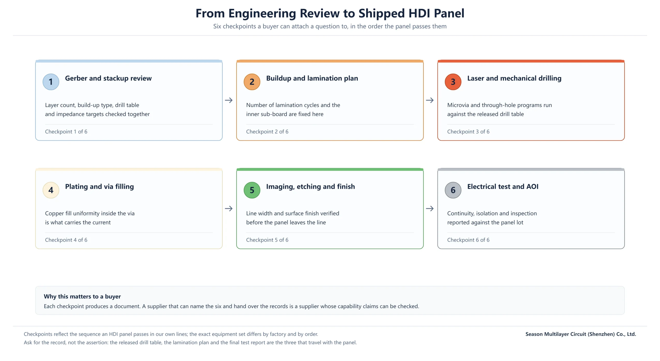
The review-to-shipment path through an HDI plant passes six checkpoints, and each one produces a document. The order matters, because each checkpoint consumes the previous one’s output: the drill program runs against the released drill table, and the test report describes the panel that actually left the line.
A buyer does not need to witness any of these steps. What you need is the ability to name them and ask for the record: the released drill table, the lamination plan, and the final electrical test report are the three that travel with the panel. A factory that can produce them on request is a factory whose capability claims can be checked — which is the entire difference between evidence and advertising.
Laser Drilling and Microvia Formation Explained
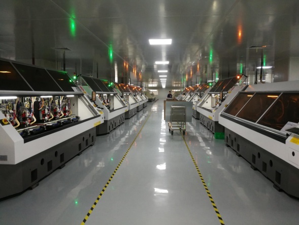
Laser drilling is the step that defines HDI. Our production microvias run at 0.1 mm nominal diameter, with 0.076 mm achievable on engineering review — the 3–5 mil range that covers everything from smartphone-class boards to dense core modules. Blind microvias connect the outer layers one dielectric at a time, with an aspect ratio held near 1:1 so the hole plates reliably from the bottom up.
Registration is the quiet half of the specification. Layer-to-layer alignment accuracy of ±25 µm is what lets stacked vias sit on top of each other without marginal capture pads, and it is why the drilling machines and the imaging line are calibrated as a pair. On boards that mix technologies, the mechanical drilling fleet runs the through-holes and buried vias — our minimum mechanical drill and 2/2 mil line and space in production, 1.8/1.8 mil on samples, cover the fine-line side.
Via Filling, Plating and the Current They Carry
A microvia is only as good as its copper. Electroplated via fill has to grow from the bottom of the hole without leaving voids or dimples that break the stacking plan, and fill uniformity is what decides whether the via carries its intended current. This is a chemistry-and-control problem: bath management, current density and plating time are tuned per build, then verified by cross-section on coupons.
Filling and tenting serve different purposes, and a capable HDI PCB manufacturer will ask which one your design needs rather than assume. Filled and capped vias support via-in-pad layouts for BGA breakout; resin-filled vias planarize the surface for fine-pitch imaging. The relevant capability page — for example the 10-layer 2-stage HDI prototype — shows how the fill and stack choices appear in a released stackup.
Capability Ranges to Compare Across Suppliers
Capability tables are where marketing meets arithmetic. The numbers below are ours to hold, and they are the categories a qualification visit should compare — not the logo wall. Where a range has conditions attached, the conditions are the honest part of the claim.
| Capability | Batch production | Small batch / prototype | Notes |
|---|---|---|---|
| HDI stages | 1–3 stages | 4 stages; any-layer on samples | 8-layer 3-stage stacked/staggered vias in production |
| Laser microvia diameter | 0.1 mm (4 mil) | Down to 0.076 mm on review | 3–5 mil laser drilling range; blind via aspect ratio about 1:1 |
| Layer-to-layer registration | ±25 µm | ±25 µm | Laser drilling alignment accuracy |
| Line and space | 2/2 mil | 1.8/1.8 mil on samples | Fine-line imaging in production |
| Layer count | 2–30 layers | Any-layer HDI samples | Group capacity 3,000,000 m² per year |
| Heavy copper | 3 oz and above | 3 oz and above | High-current and power applications |
| Site annual capacity | 720,000 m² | — | 600,000 m² multilayer, 80,000 m² flex, 40,000 m² rigid-flex |
Two of these rows deserve emphasis. First, the difference between batch and prototype capability is real: any-layer HDI on samples does not mean any-layer in volume, and a supplier who blurs that line is borrowing tomorrow’s process against today’s order. Second, capacity figures describe a factory’s ability to hold your slot when your reorder arrives — the reason they belong on a capability table at all.
Special Processes Beyond the Microvia
HDI rarely travels alone. Power domains need heavy copper at 3 oz and above; back-plane style assemblies need back-drilled stubs; packaged products need countersunk and stepped holes, edge plating and castellations. These processes interact with the microvia structure — a back-drill that runs past its target depth can undermine a buried via — so they belong to the same engineering review, not to a separate quote.
- Heavy copper from 3 oz upward for high-current paths and power trees.
- Back-drilling for controlled stub removal on high-speed layers.
- Countersunk, stepped and press-fit holes for mechanical assembly.
- Edge plating and metal-backed edges for shielding and grounding.
- Mixed lamination builds that combine materials with different cure profiles.
Where the product bends, the factory changes shape too. Rigid-flex construction pairs the HDI density with a flexible interconnect, and our 6-layer rigid-flex PCB shows the combination in a shipped design. Flex and rigid-flex capacity is a separate line in the capability table for a reason: the lamination, coverlay and plating controls differ from rigid work.
Impedance Control and High-Speed Work
As edge rates rise, the microvia stops being the hardest problem and the laminate becomes one. Low-loss and mid-Dk materials — with dielectric constants around 3.5 and below on selected builds — reduce insertion loss on long nets, and the stackup has to hold their geometry tightly enough for the impedance model to survive production.
| Impedance tolerance | Typical application | How it is verified |
|---|---|---|
| ±10% | General digital, industrial control and consumer interfaces | Standard coupon testing per build |
| ±8% | Memory, storage and display signal groups | Tighter etch and lamination control with coupon data |
| ±5% | High-speed differential pairs; radar and RF structures | Per-panel coupon verification and sample reports |
The tolerance table is a negotiation between physics and statistics: the tighter the band, the more the process — not the design — decides yield. On designs that push the ±5% band, expect the factory to propose coupon placement early, because verification is planned into the panel, not requested after it. A worked example from the RF side is the ZYF300CA-P radar high-frequency PCB, where the material call-out and the tolerance band travel together.
Questions That Sort a Real HDI PCB Manufacturer from a Brochure
Qualification questions work best when they ask for evidence instead of opinions. Each question below maps to a checkpoint from the review workflow above, and each has a document-shaped answer.
- How many lamination cycles does my build-up need, and which press plan holds them? (Expect a stackup proposal, not a yes.)
- What is your production microvia diameter today, and what changes at 0.076 mm? (Expect the review condition, stated.)
- Show a cross-section report from a recent stacked-via build. (Expect a coupon report with lot traceability.)
- What did the last ±5% impedance build yield, and where were the coupons? (Expect coupon data, not a certificate.)
- Which of these processes run in-house, and which are partner operations? (Expect a straight answer about drilling, plating and test.)
- What documents ship with the panel? (Expect drill table, lamination plan and final test report as the minimum.)
Certification belongs in the same conversation. Our site operates under ISO 9001 and ISO 14001 with UL recognition and IATF 16949 for automotive work — but the certificates describe the management system, while the questions above describe the process. Both matter; neither substitutes for the other. Where a customer’s audit needs a walk-through, the same 6-layer automotive PCB prototype page shows how these controls appear on a shipped, safety-adjacent design.
Frequently Asked Questions About HDI PCB Manufacturers
What layer count can an HDI PCB manufacturer support?
Our group builds 2–30 layers with HDI structures up to 4+N+4: an eight-layer sub-board carrying four sequential build-up layers on each side. Practical layer count is a stackup question rather than a machine limit — the build-up type, the microvia stages and the lamination plan decide what ships profitably, which is why the review fixes them before quoting.
How small can laser microvias go?
Production microvias run at 0.1 mm nominal — 4 mil — with 0.076 mm achievable on engineering review. The honest answer has two parts: the drill capability, and the plating window that fills the hole reliably. Below 0.1 mm, aspect ratio and fill quality narrow the process window, so those builds are reviewed stackup-by-stackup rather than quoted from a table.
What does 1-stage vs 2-stage HDI mean?
The stage count is the number of sequential build-up layers on each side of the core. A 1-stage board adds one microvia layer per side, a 2-stage board adds two, and each additional stage adds a lamination cycle. We produce 1–3 stages in batch, 4 stages in small batch, and any-layer HDI on samples — including 8-layer 3-stage builds with stacked and staggered vias.
How is impedance controlled on HDI boards?
Through a model, a coupon and a tolerance band. The stackup proposes geometry against the target — ±10% for general digital work, ±8% for memory and display groups, ±5% for high-speed differential and RF structures — and coupons on the panel verify the result against the model. Tighter bands depend more on process statistics, so coupon placement is planned into the panel layout early.
Can an HDI PCB manufacturer support rigid-flex and flex builds?
Yes when the capacity exists as a dedicated line. Our site runs 720,000 m² per year, of which 80,000 m² is flex and 40,000 m² rigid-flex; the rest is rigid multilayer. Rigid-flex shares the HDI playbook — fine lines, filled vias, controlled lamination — but adds coverlay and bending controls, so treat it as a related capability rather than the same one.
What documents should I expect an HDI factory to provide?
At minimum: the released drill table, the lamination plan, the impedance coupon report where the build calls for it, and the final electrical test and inspection records tied to the panel lot. Together they trace the board from review to shipment. A supplier who can name and produce these on request is one whose capability claims can be audited rather than believed.
Does HDI prototyping differ from HDI production?
In capability and in discipline. Prototypes can push the frontier — any-layer HDI and 0.076 mm microvias are sample-stage capabilities here — while batch production holds 1–3 stages with the tighter statistics that repeatability demands. A good factory tells you which column of the capability table your build sits in today, and what moving it to the other column would take.
Send the Stackup Before the Purchase Order
Send the Gerber data with layer count, target impedances and the environments the board will serve. The engineering team returns a build-up proposal — stages, lamination cycles, microvia plan and coupon strategy — so the quotation you compare is the one the factory can actually hold.
The review is part of our PCB manufacturing service, from a first prototype panel through production volumes.