Book Appointment Now

Which PCB surface finish fits your board? Compare HASL, ENIG, ENEPIG, OSP, immersion silver, tin and hard gold on planarity, shelf life and cost.
PCB Surface Finish Comparison: HASL, ENIG, OSP, Silver and Gold
A PCB surface finish is the last thing added to a board and the first thing that fails in the field. It protects bare copper between fabrication and assembly, then has to disappear, alloy or sit still while solder forms a joint. Get it wrong and the symptom appears months later as a pad that will not wet, a connector that wears through, or a flat pad that turned out to be a mound.
This comparison covers the eight finishes that account for nearly every order, what each one is actually good at, and where it is a poor fit. It gives you a planarity and cost view, a selection table keyed to pad pitch, contact wear and storage, and the incoming checks that catch a finish problem before it reaches the assembly line.
Table of Contents
- What a PCB Surface Finish Has to Do
- The Finishes That Cover Most Orders
- PCB Surface Finish Comparison Table
- ENIG: Flatness First, With a Black Pad Watch-Out
- OSP: Lowest Index Cost, Shortest Shelf Life
- HASL and Lead-Free HASL: Still the Volume Default
- Immersion Silver and Immersion Tin: Flat but Sensitive
- Hard Gold and ENEPIG for Contacts and Bonding
- Choosing a PCB Surface Finish by Pitch, Contact and Storage
- Where the Cost Difference Actually Comes From
- Incoming Checks That Catch Finish Problems Early
- FAQ
- Get the Finish Specified Against Your Assembly Process
What a PCB Surface Finish Has to Do
Three jobs, and most specification arguments come from trading one against another. First, protect the copper from oxidation and contamination during storage, handling and the first reflow pass. Second, present a surface that solder wets reliably within the profile your assembly process can accept. Third, stay out of the way electrically and mechanically: flat enough for fine paste deposits, hard enough for a connector that mates a few hundred times, and bondable if anything is wire bonded.
No finish does all three perfectly. HASL protects copper thickly but is uneven. OSP is flat and cheap but has the shortest shelf life. Hard gold survives repeated mating but is a poor soldering surface. The engineering decision is therefore not which finish is best, but which failure mode you can least afford in this product.
The finish is also the one item most exposed to undocumented substitution, because two builds can look identical and differ only in a micron of metal. Naming the finish, the layer thicknesses and the acceptance specification on the fabrication drawing is what keeps the manufacturing capability you reviewed the one that actually ships.
The Finishes That Cover Most Orders
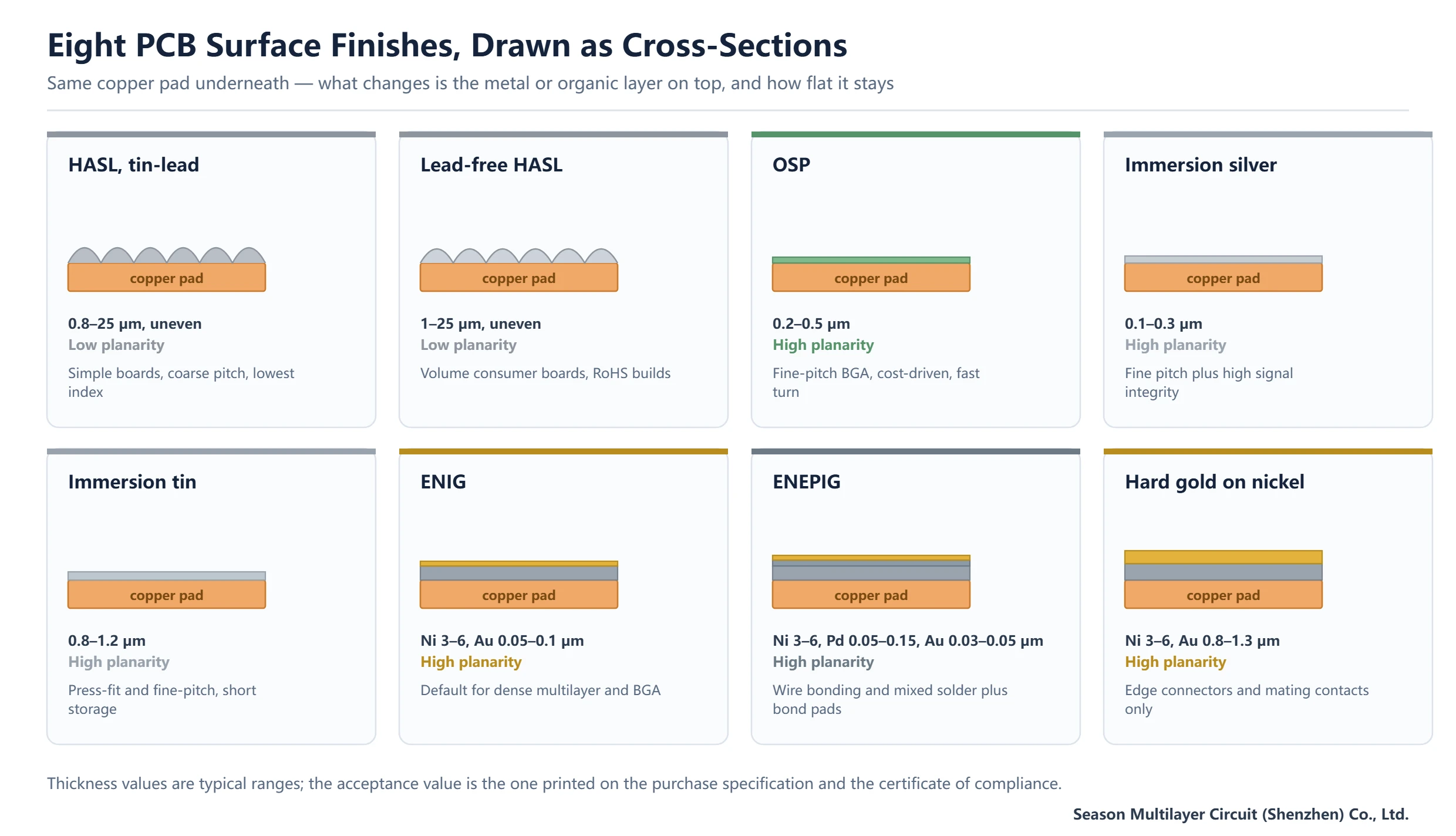
Eight finishes cover almost every order that reaches a fabrication house. HASL in its tin-lead and lead-free forms is the molten-solder approach; OSP is an organic film that protects copper without adding metal; ENIG, ENEPIG, immersion silver, immersion tin and hard gold are all metal systems with very different thicknesses and purposes.
The thickness differences matter more than the names. An ENIG gold layer at 0.05 to 0.1 µm is a protective cap over nickel, while hard gold on a connector tab runs at 0.8 to 1.3 µm because it has to survive abrasion. A PCB surface finish call that names only the family, and not the layer thicknesses, is therefore only half a specification.
The cross-sections in the figure above use the same copper pad for every finish, so the comparison is like for like: the only variable is what sits on top and how flat the result is.
PCB Surface Finish Comparison Table
The table below is the working summary. Thicknesses are typical ranges, and the relative cost index is indicative, expressed against tin-lead HASL as 1.0 for the same board area and quantity. Your quotation remains the only authoritative number for a specific build.
| Finish | Typical thickness | Planarity | Shelf life, sealed | Relative cost index | Best fit |
|---|---|---|---|---|---|
| HASL, tin-lead | 0.8–25 µm | Low | 12 months or more | 1.0 | Coarse pitch, cost-led, through-hole heavy |
| Lead-free HASL | 1–25 µm | Low | 12 months or more | 1.1–1.2 | RoHS volume builds, coarse to medium pitch |
| OSP | 0.2–0.5 µm | High | Around 6 months | 1.0–1.1 | Fine pitch, cost pressure, fast assembly |
| Immersion tin | 0.8–1.2 µm | High | 6–12 months | 1.3–1.5 | Press-fit, fine pitch, short pipeline |
| Immersion silver | 0.1–0.3 µm | High | 6–12 months | 1.4–1.7 | Fine pitch with high-frequency content |
| ENIG | Ni 3–6, Au 0.05–0.1 µm | High | 12 months or more | 1.6–2.1 | Dense multilayer, BGA, general high reliability |
| ENEPIG | Ni 3–6, Pd 0.05–0.15, Au 0.03–0.05 µm | High | 12 months or more | 2.2–3.0 | Solder plus wire bond on the same board |
| Hard gold on nickel | Ni 3–6, Au 0.8–1.3 µm | High | 12 months or more | 2.8–4.0 | Edge connectors, mating contacts, keypads |
Two readings of this table are worth carrying into a design review. Planarity separates the finishes into two groups, and pitch is what forces the choice between them. Cost index separates them again, and the spread between the cheapest and the most expensive option is roughly a factor of three to four on the finish step alone, not on the whole board.
Acceptance criteria for the metal systems are defined in the IPC finish specifications, with ENIG, ENEPIG, immersion silver and immersion tin each having a dedicated document and IPC-6012 covering the finished board. The current index is published at the IPC standards library.
ENIG: Flatness First, With a Black Pad Watch-Out
ENIG deposits nickel-phosphorus over the copper, then a thin gold layer that protects the nickel from oxidation and keeps the surface solderable. Because both layers are thin and conformal, the pad stays as flat as the copper underneath, which is why it became the default for dense multilayer boards and BGA footprints.
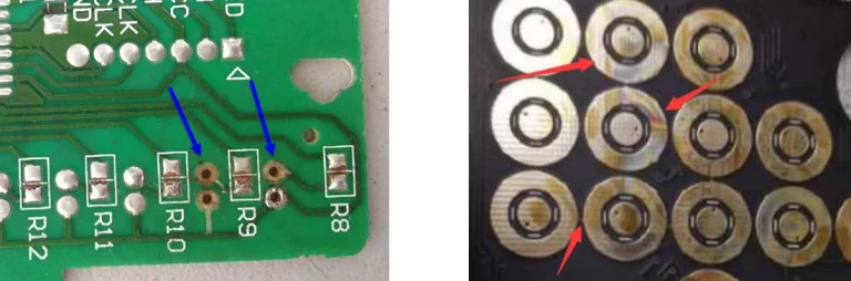
Its known failure mode is black pad, a hyper-corrosion of the nickel surface during immersion gold that leaves a brittle, poorly wetting interface. The joint may look acceptable and then crack in thermal cycling. Control comes from the nickel bath and the gold bath chemistry, not from the gold thickness, so an incoming inspection that only measures gold is measuring the wrong layer.
Our own experience with wetting failures, the causes behind them and how they are isolated in production is written up in the ENIG solderability failure guide. If you specify ENIG, ask for the nickel thickness and the phosphorus content rather than only the gold figure.
OSP: Lowest Index Cost, Shortest Shelf Life
OSP is an organic film grown on clean copper, typically a few tenths of a micron thick. It adds no metal, so the pad is as flat as the copper, and it costs almost nothing relative to the metal finishes. That combination makes it attractive for fine-pitch boards where cost pressure is real.
The constraint is time and handling. The film wears off with repeated handling, degrades with heat exposure, and has to be removed by the flux during soldering for the joint to form. Storage discipline therefore matters more than with any other finish: sealed packaging, desiccant, first-in-first-out, and a shelf life that is shorter than most planning systems assume.
Multiple reflow passes are the other risk. A board that goes through two or three assembly cycles may lose enough film to expose copper before the final pass. The storage and handling rules that keep OSP pads solderable are set out in the OSP shelf life guide.
HASL and Lead-Free HASL: Still the Volume Default
Hot air solder levelling floods the board with molten solder and blows it off with air knives, leaving a solder layer that varies from thin on fine features to thick mounds on large pads. It is robust, forgiving of copper oxidation, and by far the cheapest option, which is why it still dominates high-volume consumer and through-hole-heavy work.
The weakness is geometry. A mound a few tens of microns high is irrelevant at 1.0 mm pitch and fatal at 0.4 mm, because the stencil cannot deposit consistent paste onto a curved surface and the part may lift or tombstone. HASL also thermal-shocks the board, which is worth remembering for thin cores and high layer counts.
Lead-free HASL replaces tin-lead with a tin-silver-copper alloy and runs at a higher temperature. It solves the RoHS question without changing the process logic, and the planarity penalty is the same. If the board has a fine-pitch BGA on one side and coarse through-hole on the other, the practical answer is usually to move the whole board up to a flat finish rather than mix.
Immersion Silver and Immersion Tin: Flat but Sensitive
Immersion silver deposits a very thin silver layer directly on copper. The surface is flat and the joint forms readily, and at high frequency a silver surface avoids the nickel layer that ENIG introduces, which is why some high-speed designs prefer it. Its weakness is atmospheric sulfur: exposed silver tarnishes, and a heavily tarnished pad wets poorly. Sulfur-absorbing interleaving paper in the packaging is not optional.
Immersion tin is the press-fit and fine-pitch favourite. It provides a thin, flat, solderable layer that suits compliant-pin connectors, and the process is simple. The trade-offs are storage and whisker risk: tin is prone to forming conductive filaments over time, and the coating is thin enough that handling damage matters. Keep the storage window short and the handling clean.
Both finishes belong in the same conversation as the assembly process. A board that will sit in a warehouse for a year is a poor candidate for either, and a board that goes straight to assembly within weeks is a good one.
Hard Gold and ENEPIG for Contacts and Bonding
Hard gold is a nickel layer plus a thick gold layer hardened with a small amount of cobalt or nickel. It exists for abrasion: edge connector tabs, mating contacts and keypads that see repeated insertion. The thickness is an order of magnitude above ENIG, and that thickness is what buys the wear life. It is also a poor soldering surface, so gold fingers are specified as contacts, not as solderable pads.
Boards that need both a connector tab and solderable pads commonly combine finishes: hard gold on the tab, ENIG on the rest. That split is routine, but it has to be drawn explicitly with the gold area defined, because it adds process steps and a masking operation. Our 10-layer M.2 SSD build is a typical example of gold fingers specified alongside fine-pitch solderable pads.
ENEPIG inserts a palladium layer between nickel and gold. It solves two problems at once: the palladium barrier suppresses the nickel corrosion that causes black pad, and the surface accepts both solder and gold or aluminium wire bonding. That versatility is why it is the standard choice when a board carries bond pads, and why its cost index sits above ENIG. The trade-offs are covered in the ENEPIG selection guide.
Choosing a PCB Surface Finish by Pitch, Contact and Storage
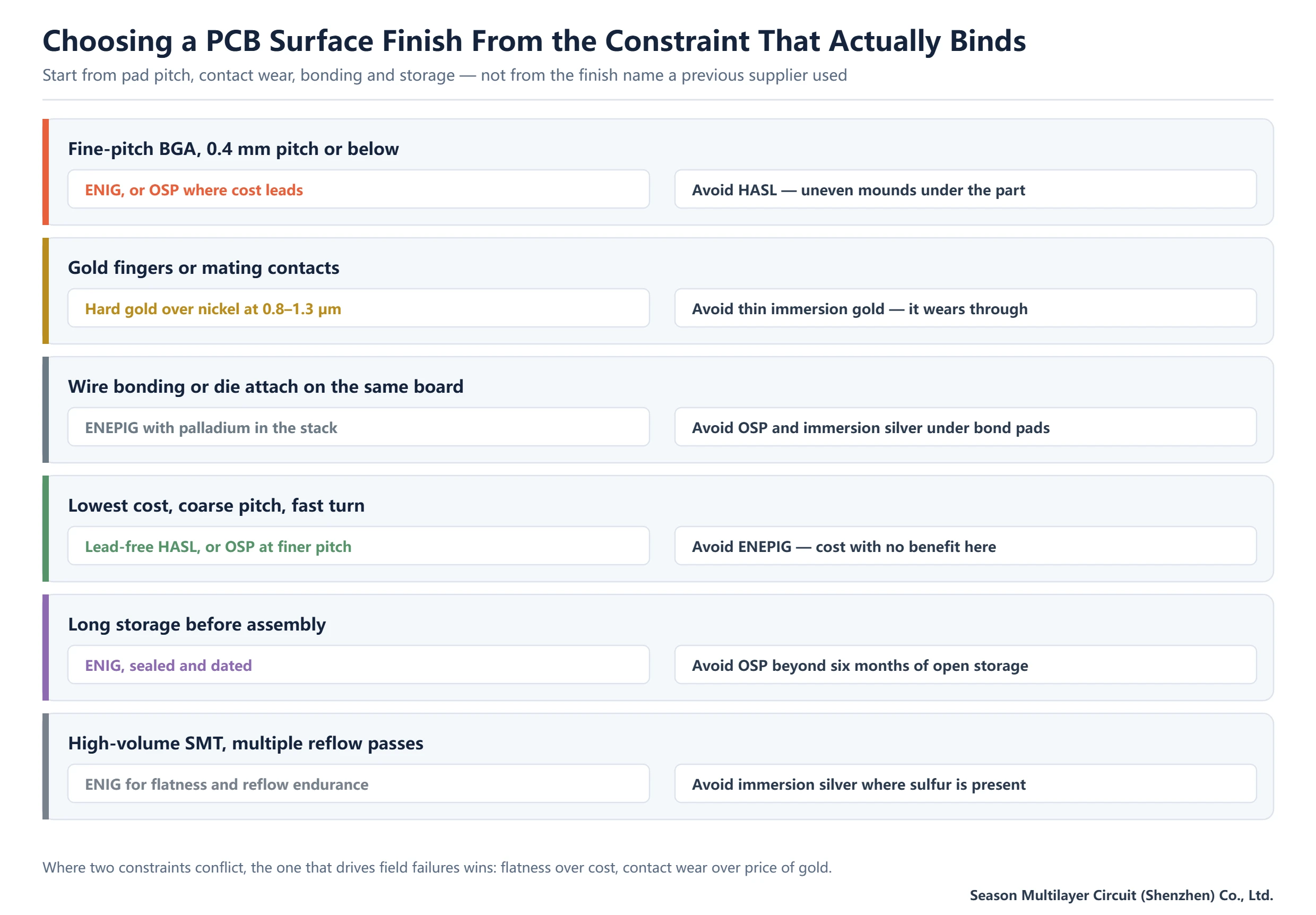
The fastest route to a defensible choice is to start from the binding constraint rather than from a preferred finish. Pad pitch rules out HASL early. Connector wear rules in hard gold. Bond pads rule in ENEPIG. Storage duration and reflow count decide whether OSP is safe. The mapping below turns those constraints into a first choice and an option to avoid.
| Constraint that binds | First choice | Acceptable alternative | Avoid |
|---|---|---|---|
| 0.4 mm pitch BGA or finer | ENIG | OSP if the board ships quickly | HASL of either type |
| Edge connector with repeated mating | Hard gold on nickel | ENIG for low mating counts only | Thin immersion gold on contacts |
| Bond pads and solder pads on one board | ENEPIG | Split finishes by area | OSP or immersion silver under bond pads |
| Lowest index cost at coarse pitch | Lead-free HASL | OSP at medium pitch | ENEPIG, hard gold |
| Storage beyond six months | ENIG | Immersion tin within its window | OSP, immersion silver in sulfur environments |
| High-frequency traces with fine pitch | Immersion silver | ENIG | HASL, thick metal stacks |
Where two constraints conflict, resolve with the cost of the field failure rather than the cost of the finish step. A worn connector or a non-wetting BGA pad costs far more than the difference between the cheapest and second-cheapest finish, so flatness and wear resistance normally win over price at the pad.
Where the Cost Difference Actually Comes From
The finish step is a small share of a finished board, but a PCB surface finish change moves that share by a large multiple. Three factors drive it: metal cost per unit area, the number of wet process steps and their control requirements, and the yield risk of the process itself. Gold and palladium systems sit at the top because of the metals; OSP and HASL sit at the bottom because the chemicals are cheap and the lines are fast.
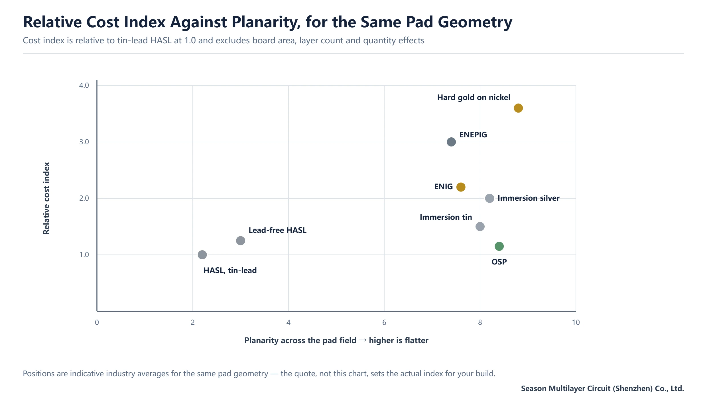
The chart above is the shortcut most buyers need: the vertical axis is the relative cost index and the horizontal axis is planarity. OSP occupies the flat-and-cheap corner, HASL the cheap-but-uneven corner, and the gold systems the flat-but-expensive region. Nothing in the expensive region becomes flat as a result of the money; flatness there comes from the process, not the price.
| Cost factor | Effect on the finish step | Where it shows up in quoting |
|---|---|---|
| Metal consumed per unit area | Gold and palladium systems are metal-dominated | Finish line item scales with plated area |
| Number of wet steps | ENEPIG adds a palladium bath and rinse train | Setup effort and minimum line loading |
| Process control burden | Black pad control in ENIG needs tighter bath management | Scrap and rework allowance, not list price |
| Selective application | Hard gold on a defined area adds masking and a second pass | Separate line item for the connector zone |
| Board area and quantity | All finishes amortise setup over more area | Panel utilisation and lot size |
Incoming Checks That Catch Finish Problems Early
A finish problem is cheap to catch at goods-in and expensive to catch after reflow. These are the checks that need no laboratory and that catch most of the real cases.
- Confirm the certificate of compliance names the finish and the layer thicknesses, not just the finish family
- Read the thickness with X-ray fluorescence on a coupon or a scrap area, and compare with the drawing
- Inspect gold areas under magnification for discoloration that suggests nickel corrosion beneath
- Check immersion silver boards for tarnish and confirm the sulfur-absorbing interleaving is present in the bag
- Verify packaging, desiccant and date coding for OSP, where shelf life is the dominant risk
- Solder a sample pad with the production flux and profile before releasing the lot to the line
Recording those results per lot turns a subjective argument into a trend. It also feeds the same report package that documents routine quality inspection, so the finish data sits beside panel, drill and electrical results rather than in a separate file nobody reviews. Where the finish interacts with mask openings and pad geometry, the checks belong with the solder mask specification, because a PCB surface finish and its mask opening are reviewed against the same pad dimensions.
Frequently Asked Questions
Which PCB surface finish should I specify by default?
For a dense multilayer board with BGA parts, ENIG is the safe default because it is flat, has a long shelf life and is widely available. For coarser through-hole work where cost leads, lead-free HASL is fine. For fine pitch on a tight budget with a fast assembly pipeline, OSP works well as long as storage is controlled.
What is the difference between ENIG and ENEPIG?
ENIG is nickel plus a thin gold cap. ENEPIG inserts a palladium layer between them, which suppresses the nickel corrosion behind black pad and makes the surface suitable for both soldering and wire bonding. ENEPIG costs more because of the extra bath and the palladium, and is chosen when the same board carries bond pads.
Why is HASL bad for fine-pitch components?
The air-knife process leaves solder mounds that vary in height across the pad field. At 0.4 mm pitch a mound of a few tens of microns is enough to make paste deposition inconsistent and to lift a part during reflow. Flat finishes such as ENIG, OSP or immersion silver avoid the geometry problem entirely.
How long can an OSP board be stored?
Roughly six months in sealed packaging with desiccant, and less once the bag is opened. The organic film wears with handling and degrades with heat, so repeated reflow passes and open storage both reduce the margin. Plan first-in-first-out release and confirm the date code before the assembly slot is booked.
Is hard gold the same as ENIG gold?
No. ENIG gold is a thin protective cap of about 0.05 to 0.1 µm over nickel. Hard gold is 0.8 to 1.3 µm of gold hardened with cobalt or nickel, applied for abrasion resistance on connector tabs. Hard gold is a contact surface, not a solderable one, and the two are usually combined on the same board.
Does the surface finish affect high-frequency performance?
It can. At high frequency current concentrates near the surface, so the metal stack matters: a nickel layer under gold adds loss compared with a silver or OSP surface. For most digital boards the effect is small, but on long high-speed traces it belongs in the stackup discussion rather than being decided by cost alone.
Can I mix two finishes on one board?
Yes, and it is common: hard gold on a connector tab with ENIG on the solderable area. The gold zone has to be defined on the drawing, because selective plating adds masking steps and a second process pass. Mixing is worth it when the alternative is an expensive finish over the whole board for the sake of a small contact area.
Get the Finish Specified Against Your Assembly Process
Send the stackup, the smallest pitch on the board and how the boards will be stored and assembled, and our engineering team will confirm the finish, the layer thicknesses and the acceptance criteria before the quotation is issued. That is also the point where a mixed finish or a shelf-life constraint gets flagged. See how we handle finish and process review or submit your Gerber data for a first pass.