Book Appointment Now

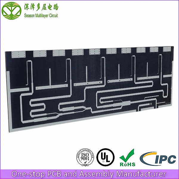
Double-sided high-frequency PTFE PCB on genuine Taconic laminate, 3.2 mm heavy build, 6/6 mil controlled impedance, immersion silver finish - built for RF, microwave, and test-instrumentation front-ends.
Double-sided High-Frequency PTFE PCB
Double-sided high-frequency PTFE PCB on genuine Taconic laminate: stable low Dk/Df through 10 GHz, 3.2 mm heavy build, 6/6 mil fine-line CPW routing, immersion silver finish — engineered for RF, microwave and test-instrumentation front-ends.
This double-sided high-frequency PTFE PCB is built on Taconic high-frequency laminate, finished at 3.2 mm with 1 oz copper on both sides. Plated through-holes at 0.5 mm minimum and 6/6 mil line/space geometry carry 50 Ω GCPW and CPW structures, while the immersion silver finish preserves low-loss pad interfaces for gold-wire and solder attachment. The 107 × 40 mm single-up panel is a production-proven format for RF power modules and antenna feed networks.
PTFE (polytetrafluoroethylene) laminates set the benchmark for microwave boards: a dielectric constant that barely moves with frequency, a dissipation factor several times lower than standard FR4, and stable performance from -55 °C to +260 °C. As 5G backhaul, radar front-ends, and point-to-point radios push deeper into the millimeter-wave region, designers are migrating from FR4 to PTFE, and Season PCB manufactures double-sided and multilayer PTFE boards on Taconic, Rogers, Arlon, and domestic F4B laminates with material in stock.
2-Layer
PTFE
3.2 mm
Board Thickness
1 oz Cu
Both Sides
0.5 mm
Min PTH
10 GHz
Stable Dk/Df
UL (E305905)
IPC-A-600 Class 2/3
ISO 9001:2015
IATF 16949
RoHS / REACH
100% E-Test
Stackup and Construction of the Double-sided PTFE PCB
The double-sided PTFE stackup is deliberately simple: two copper layers bonded to a solid PTFE core, because at high frequency, fewer interfaces mean lower loss and more predictable impedance:
- L1 / L2 (Double-Sided Outer Layers, 1 oz Copper): Both outer layers are finished at 1 oz (35 µm) copper, carrying coplanar waveguide (CPW/GCPW) feed lines, ground planes, and component pads for RF modules.
- Solid PTFE Core (Taconic High-Frequency Laminate): The solid PTFE core provides a homogeneous dielectric with no glass weave skew and no resin-rich or resin-starved zones, so impedance and phase stay uniform across the whole 107 × 40 mm panel.
- 0.5 mm Plated Through-Holes Spanning L1-L2: 0.5 mm minimum plated through-holes stitch the top ground to the bottom ground with low-inductance via fences around every signal transition.
- 6/6 mil Fine Lines for Dense CPW Routing: 6/6 mil minimum line/space is the fine-line capability of this platform, keeping CPW and GCPW feed networks compact. On a 3.2 mm PTFE core the coplanar gap, not the dielectric height, sets the impedance: a 50 Ω microstrip on this build would need a ~10 mm trace.
- 3.2 mm Heavy Build for RF Power Modules: The 3.2 mm finished thickness delivers mechanical rigidity for connector-rich assemblies and high-power RF modules mounted without additional chassis.
- Immersion Silver Finish for Low-Loss Pads: Immersion silver (0.05–0.15 µm over nickel-free surface) gives a flat, low-loss, solderable finish that suits both reflow and gold-wire bonding processes.
- Custom Laminate / Copper / Thickness Options: Stackup is fully customizable: alternative PTFE laminates (Rogers RT/duroid, Arlon, F4B), copper weights, and thicknesses are available to match your impedance and loss budget.
This 2-layer double-sided high-frequency PTFE PCB stackup is a production-proven reference for RF, microwave, and instrument front-end boards. Our RF engineering team tunes the laminate grade, copper weight, and dielectric thickness to your impedance target and insertion-loss budget. All of it runs on a single lamination cycle for the lowest possible cost on double-sided PTFE prototypes and production.
Why PTFE Instead of FR4 or Hydrocarbon Ceramic?
For a double-sided high-frequency PTFE PCB, laminate choice decides insertion loss before a single trace is etched. The three substrate families overlap in capability but diverge quickly in loss, cost and process behavior.
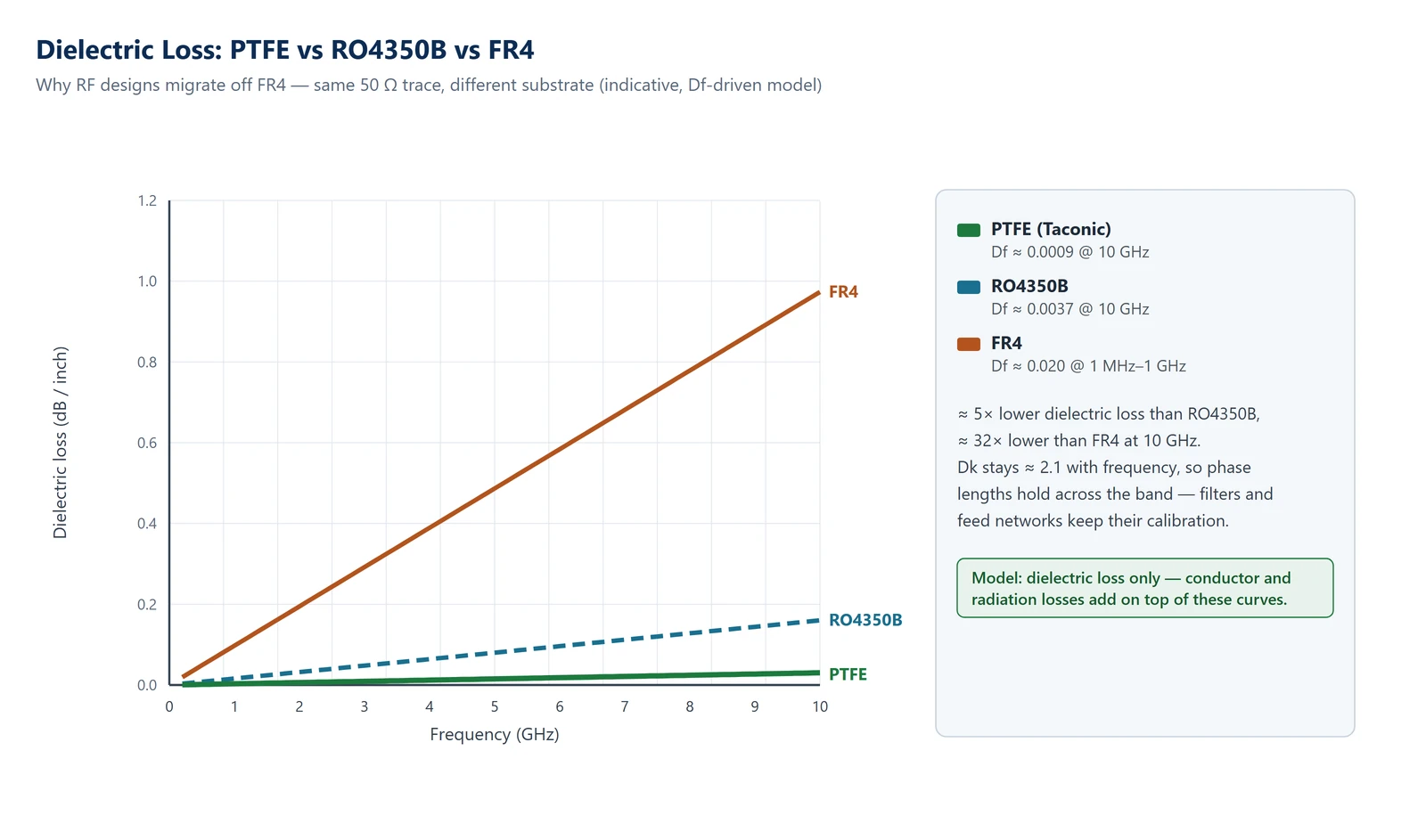
FR4 is the cheapest and easiest to fabricate, but its dissipation factor near 0.020 turns dielectric loss into the dominant loss term above a few GHz, and its woven-glass construction makes Dk uneven at fine feature scales. Hydrocarbon ceramic laminates such as RO4350B cut Df to about 0.0037 and process almost like FR4, which is why they dominate base-station power-amplifier boards. PTFE pushes Df down to about 0.0009 with a nearly frequency-flat Dk near 2.1, the lowest-loss and most phase-stable option of the three. The trade-off is softer mechanics and a more specialized fabrication flow.
| Property | PTFE (typical) |
|---|---|
| Df @ 10 GHz | ≈ 0.0009 (grade dependent) |
| Dk stability vs frequency | nearly flat (≈ 2.1) |
| Moisture absorption | < 0.1 %, effectively non-hygroscopic |
| Processing | specialized: activation, plasma desmear, per-lot scaling |
| Relative cost per panel | highest of the three |
| Typical use | mmWave feeds, high-Q filters, phase-critical arrays |
Where does that leave a decision? Below roughly 3 GHz, a good FR4 stack often meets the loss budget and the cost argument wins. Between 3 and 10 GHz, RO4350B and similar hydrocarbon ceramics are usually the pragmatic middle ground. Once the budget tightens (long feed runs, high-Q filters, millimeter-wave bands, or phase-critical arrays), a double-sided high-frequency PTFE PCB recovers the margin that FR4 and even RO4350B give away. Our RF engineering team models your trace geometry against all three laminate families before you commit; the full selection logic is in our high-frequency PCB materials and Dk/Df selection guide.
Technical Capability & Specifications
| Layer Count | 2 layers (double-sided) |
| Base Material | PTFE (Polytetrafluoroethylene) high-frequency laminate |
| Material Grade | Taconic (Rogers, Arlon, F4B, Isola alternatives available) |
| Finished Thickness | 3.2 ± 0.32 mm |
| Panel Size | 107 × 40 mm (single-up) |
| Outer Copper Weight | 1 oz (35 µm) on both sides |
| Min Plated Through-Hole | 0.5 mm |
| Min Line / Space | 6 / 6 mil (0.15 / 0.15 mm) |
| Surface Finish | Immersion silver (0.05–0.15 µm over nickel-free surface) |
| Operating Temperature | −55 °C to +260 °C |
| Dielectric Constant (Dk) | ≈ 2.1 (PTFE), stable across frequency |
| Dissipation Factor (Df) | ≈ 0.0009 at 10 GHz (PTFE, grade dependent) |
| Impedance Control | 50 Ω GCPW / CPW, ±10 % (coupon-tracked) |
| Solder Mask | Not required (PTFE boards typically left unmasked for RF) |
| Legend / Marking | Optional, epoxy ink or laser marking |
| Operating Frequency | DC to 40 GHz (laminate dependent) |
| Acceptance Standard | IPC-A-600 Class 2 (default) / Class 3 (on request) |
| Quality System | ISO 9001, UL, RoHS, IPC |
Key Advantages of Our Double-sided High-Frequency PTFE PCB
- Genuine Taconic PTFE Laminate: Genuine Taconic PTFE laminate with a stable dielectric constant and ultra-low dissipation factor, for several times lower insertion loss than FR4 at microwave frequencies.
- −55 °C to +260 °C Operating Range: Reliable performance from -55 °C to +260 °C: PTFE keeps its electrical and mechanical properties where FR4 delaminates, making it suitable for outdoor RF hardware and high-temperature electronics.
- Outstanding Chemical Resistance: Outstanding chemical resistance: PTFE withstands acids, alkalis, and solvents that attack conventional laminates, ideal for industrial and chemical-processing environments.
- Non-Moisture-Absorbing Dielectric: Non-moisture-absorbing substrate: dielectric properties stay stable in humid environments, so antenna and outdoor RF hardware holds calibration over years of service.
- Heavy 3.2 mm Mechanical Build: Heavy 3.2 mm double-sided PTFE PCB build at 1 oz copper handles the thermal and mechanical loads of high-power RF amplifiers without extra support plates.
- Immersion Silver RF-Friendly Finish: Immersion silver finish offers low contact resistance and excellent solderability at lower cost than ENIG, with RF-friendly loss characteristics across the microwave band.
Overcoming Critical Challenges in Double-sided PTFE PCB Manufacturing
1. PTFE Surface Metallization and Copper Adhesion
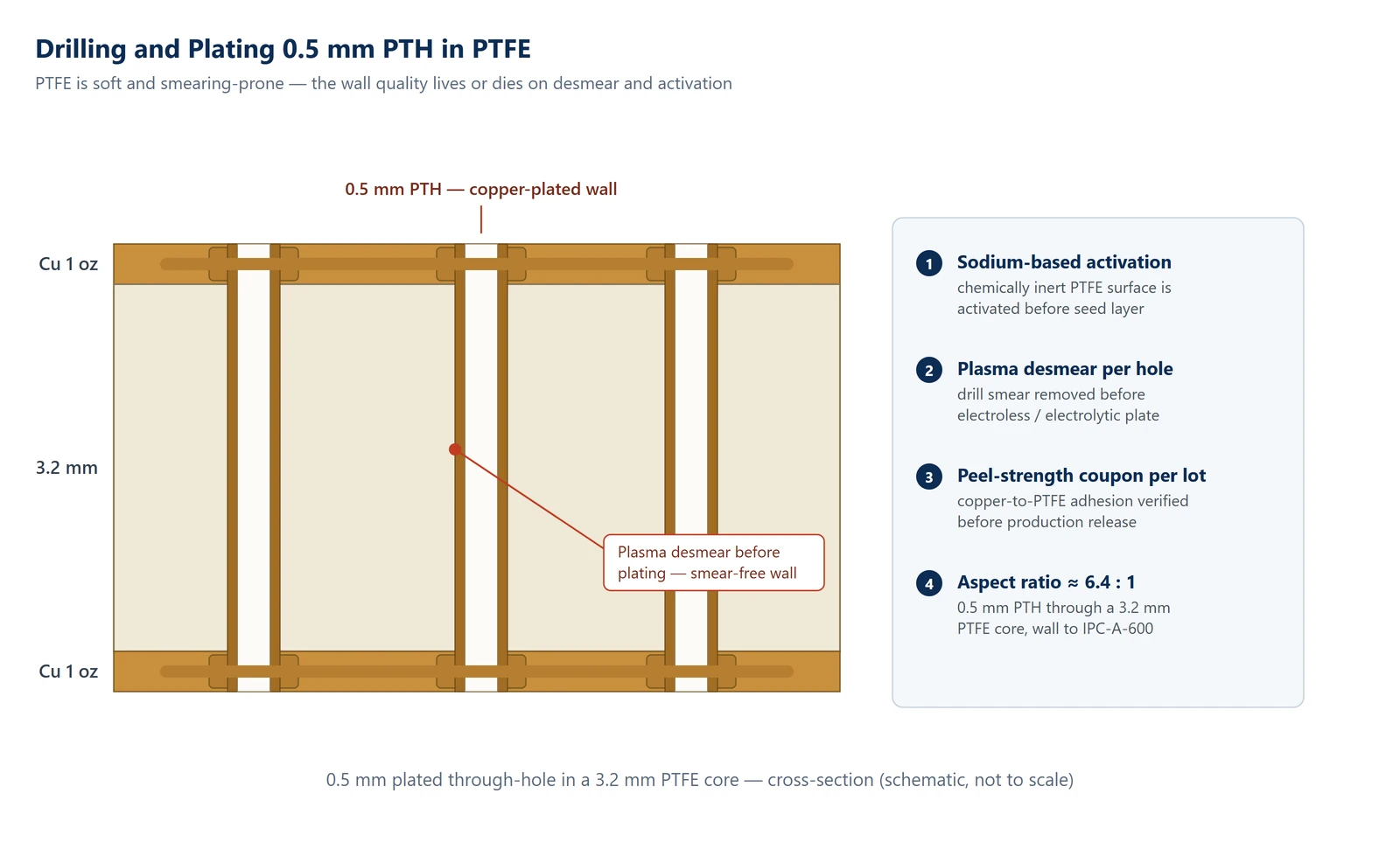
PTFE is notoriously difficult to metallize: its chemically inert surface resists adhesion. We run sodium-based surface activation followed by controlled sputtered/electroless seed layers, and peel-strength coupons verify copper adhesion on every PTFE lot before production release.
2. Drilling and Plating 0.5 mm PTH in PTFE
Drilling PTFE is smearing-prone: the soft resin smears onto hole walls and kills plating adhesion. Our process controls spindle speed, feed rate, and hit count, then desmears every hole before plasma treatment, delivering reliably plated 0.5 mm through-holes with copper walls exceeding IPC-A-600 Class 2 requirements.
3. Dimensional Control on 3.2 mm PTFE Builds
The 3.2 mm thick, 107 × 40 mm panel concentrates dimensional-control pressure: PTFE’s high CTE can distort fine-pitch patterns during lamination cycles. We compensate artwork scale per laminate lot, monitor etch-back on first-article, and verify finished dimensions and impedance on coupons processed with your panel.
How We Verify Impedance and Pad Quality on PTFE Builds
Impedance is verified the same way on every double-sided high-frequency PTFE PCB: coupons processed alongside your production panels, TDR-measured against the stackup model, and reported with the shipment. Because PTFE laminates vary slightly by grade and lot, the coupon result, not the datasheet value, is what we sign off against ±10 %, with ±8 % and ±5 % available on request. The measurement method and reporting format follow our PCB impedance measurement methods, so your SI team can compare numbers directly against your simulation. The coupon plan covers all critical impedance structures on the panel, not a sample.
The immersion silver finish stays the default for RF pads on this double-sided high-frequency PTFE PCB: silver plates directly on copper with a flat, low-loss interface, lower contact resistance than ENIG, and suitable pad designs tolerate gold-wire bonding. Where shelf life or mixed-technology assembly demands a nickel barrier, we also quote ENIG and immersion tin. The trade-offs follow the same logic as our surface finish comparison.
Where Our Double-sided High-Frequency PTFE PCBs Are Used
- Radar & Microwave Front-Ends: Radar and microwave front-ends: local oscillator distribution, power-divider trees, and low-noise receiver boards that depend on PTFE’s phase stability for beam accuracy.
- High-Reliability Industrial RF: industrial RF generators and process-heating electronics, where the -55 °C to +260 °C temperature envelope and low-outgassing laminate keep RF chains aligned through thermal cycling.
- 5G Backhaul & Point-to-Point Radios: 5G backhaul and point-to-point radios: antenna feed networks, filter modules, and duplexer boards operating in the 6–40 GHz range with minimal insertion loss.
- Test & Measurement Instrumentation: Test and measurement instrumentation: VNA fixtures, probe stations, and calibration standards that rely on the repeatable dielectric constant of a solid PTFE core.
- Chemical & Process-Heating Plants: chemical-processing and process-heating electronics on a double-sided high-frequency PTFE PCB, where high operating temperatures meet corrosive atmospheres and both the PTFE dielectric and the immersion silver pads survive the acid, alkali, and solvent exposure that destroys FR4 assemblies.
DFM Checklist Before You Release PTFE Gerbers
A double-sided high-frequency PTFE PCB quote is only as accurate as the data behind it. These eight items separate a clean release from a week of back-and-forth, and every one of them is checked during engineering review:
- Laminate grade and thickness stated explicitly (for example Taconic 3.2 mm), not just “PTFE”.
- Impedance structures defined as CPW/GCPW trace-and-gap pairs, not only the 50 Ω target value.
- RF stitch-via fences drawn as real vias with pitch, not indicated by a note.
- Copper balance symmetric between L1 and L2 so the 3.2 mm core stays flat after lamination.
- Panel orientation and breakaway rails called out if the 107 × 40 mm format ships single-up.
- Surface finish specified per pad function: solder pads, wire-bond pads, connector lands.
- Gold-wire-bond pads flagged with pad size and wire diameter so the silver plating stack is adjusted.
- A stackup drawing attached, even a sketch, so impedance modelling starts from your intent.
For the drilling side of the checklist (hit counts, entry and backing material, and aspect-ratio limits), see our PCB drilling process comparison. For laminate substitution questions, the laminate selection guide covers the full decision tree, and builds that pair PTFE with FR4 are covered in our hybrid PCB stackup guide.
Our Quality Guarantee for High-Frequency PTFE PCBs
Every double-sided high-frequency PTFE PCB passes a quality gate system refined across two decades of RF and microwave manufacturing:
- 100% electrical test on every board with net-list comparison against your Gerber/ODB++ source
- Controlled-impedance coupons processed alongside production panels, measured with TDR and reported with shipment
- Peel-strength verification of copper-to-PTFE adhesion on every laminate lot
- Micro-section inspection of plated through-holes for copper thickness, etch-back, and smear removal
- AOI on both copper layers plus visual inspection under magnification at the RF edge-coupled structures
- IPC-A-600 Class 2/3 workmanship acceptance, class selectable per order
- Full traceability from laminate lot to shipped board, with CoC, material certificates, and inspection reports on request
Why Choose Season PCB for Your Double-sided High-Frequency PTFE PCB?
Season PCB (998PCB Group, established in 2006) manufactures the double-sided high-frequency PTFE PCB platform and high-speed boards on a dedicated RF line, with Rogers, Taconic, Arlon, F4B, and Isola laminates stocked year-round. That material availability is what keeps our RF prototype lead times short.
Here is what every double-sided high-frequency PTFE PCB we ship is backed by:
- Deep RF laminate inventory — Taconic, Rogers, Arlon, F4B, and Isola in stock, so your high-frequency prototype does not wait on material procurement
- Free DFM review on every quote, including impedance modeling and stackup-loss estimation from our RF engineering team
- Fast prototypes: double-sided PTFE samples typically in 5–7 working days, confirmed at engineering review, with expedite options for measurement-lab deadlines
- One-stop scaling from prototype to mass production, including RF module PCBA assembly and functional test
- Free sample support for qualified high-frequency projects — ask our team for conditions
- Engineering support in both English and Chinese across the 998PCB Group channel
Season PCB specializes in double-sided high-frequency PTFE PCB manufacturing for RF, microwave, and front-end modules — from radar and phased-array chains to 5G backhaul and instrumentation. Our double-sided high-frequency PTFE PCB build-up features genuine Taconic high-frequency laminate, 3.2 mm heavy build, 6/6 mil controlled-impedance routing, and immersion silver finish for low-loss pad interfaces.
For adjacent double-sided high-frequency PTFE PCB builds and other RF platforms, our double-sided Rogers high-frequency PCB page covers the RO4350B platform, and our radar-grade high-frequency PCB page goes deeper on laminate-specific processing. The factory behind both lines is described in our process capability overview, and material availability is summarized on the PCB materials and laminates page.
For your high-frequency project, Season PCB provides fast turnaround, stackup-first engineering support, and ISO-certified quality. 998PCB Group, established in 2006, supports the same program from PTFE prototype to mass production across both English and Chinese channels.
Our double-sided high-frequency PTFE PCBs are built to high-speed and high-frequency PCB manufacturing standards and can scale into high-layer-count PCB mass production, or be paired with one-stop PCBA assembly service covering RF module placement and module-level testing. Pair these PTFE boards with our broader High Frequency PCB product line for the rest of your microwave and RF projects.
Frequently Asked Questions
What is a double-sided PTFE PCB?
It is a two-layer circuit board built on a PTFE (polytetrafluoroethylene) laminate instead of FR4: copper foil bonded to both sides of a solid PTFE core, connected by plated through-holes. PTFE’s dielectric constant (around 2.1) stays nearly flat with frequency and its dissipation factor is far lower than FR4, making the double-sided high-frequency PTFE PCB the standard choice for CPW and microstrip RF circuits, antenna feeds, and microwave modules.
Why choose Taconic PTFE laminate?
Taconic is one of the most widely qualified PTFE laminate brands in RF production, with tightly controlled dielectric constant (tolerances down to ±0.02 on selected grades) and proven batch-to-batch repeatability. That predictability matters for filters and phased-array networks where impedance errors translate directly into ripple and beam errors. We also work with Rogers, Arlon, F4B, and Isola if your design specifies a different laminate.
Is a 3.2 mm PTFE board difficult to manufacture?
Thickness adds process risk: deep holes need longer plating times, drill smear is harder to remove, and the soft PTFE core can shift during lamination. We qualify every thick PTFE build with first-article micro-sections, per-lot artwork scaling, and impedance coupons, so the 3.2 mm board you receive matches the stackup your simulation assumed.
What is the typical lead time for double-sided PTFE PCBs?
Because we stock Taconic and other high-frequency laminates, standard double-sided high-frequency PTFE PCB prototypes typically ship in 5–7 working days after engineering approval, confirmed at engineering review. Volume production typically runs 10–15 working days depending on quantity and test requirements. Send your Gerber files and stackup for an exact schedule and quote.
Can you build multilayer PTFE boards, or only double-sided?
The double-sided high-frequency PTFE PCB is the volume format on this platform, but multilayer PTFE builds are quoted against your stackup: bonded PTFE cores, or hybrid stacks that pair a PTFE layer with FR4 wings for cost and rigidity. Hybrid constructions are the common middle ground — see our hybrid PCB stackup guide for how mixed-dielectric builds are laminated and what they change for impedance modelling.
How does immersion silver compare with ENIG on a double-sided high-frequency PTFE PCB?
Silver plates directly on copper with a flat, low-loss interface, which is why it stays the default on this double-sided high-frequency PTFE PCB: lower contact resistance, lower cost, and no nickel layer adding series loss at the pad. ENIG brings a nickel barrier and a longer shelf life, which mixed-technology assemblies sometimes need. The full finish trade-off matrix, including ENEPIG, is in our surface finish selection guide.
What does a double-sided high-frequency PTFE PCB quote need from your side?
Gerber or ODB++ data, a stackup drawing with the target trace and gap geometry, the impedance value and tolerance, and the operating frequency range. With those four items we model the CPW/GCPW structures, confirm the coupon plan, and return the stackup drawing and quote within 24 hours — the same TDR measurement loop described in our impedance measurement methods guide.
Can PTFE boards be panelized with FR4 service rails?
Yes. The common approach for a double-sided high-frequency PTFE PCB panel is a hybrid build: PTFE in the active area, FR4 rails bonded or mechanically fixed for handling and SMT conveyor compatibility. Panel-level planning affects edge plating and depaneling, so flag it at quotation — our hybrid stackup guide shows how the mixed-dielectric panel is built and what it changes for assembly.
Ready to start your double-sided PTFE high-frequency project?
To receive a formal quote for your double-sided high-frequency PTFE PCB, send your Gerber or ODB++ files, board outline (DXF preferred), target impedance, and operating frequency range. Whether you need 5 pieces for an RF lab prototype or 5,000 modules for a network rollout program, our engineering team responds within 24 hours with DFM feedback, a stackup drawing, and a quote.