Book Appointment Now

What an ABF substrate is, how Ajinomoto build-up film enables sub-10 µm lines for CPU and GPU packages, and how it differs from BT and FR-4 — for hardware buyers.
ABF Substrate Explained: Build-Up Film, Fine Lines and FC-BGA
Every CPU, GPU, AI accelerator, and high-pin-count FPGA shipped today sits on an ABF substrate — a package substrate built from a photo-imageable dielectric film that can define lines finer than a bacterium is long. Yet because the film lives inside the package, most hardware teams never see it until a board fails qualification or a quote comes back unexpectedly expensive.
This guide explains what an ABF substrate is, where the build-up film came from, why it enables the fine-line geometry that processor packages require, and how it differs from BT substrates and conventional FR-4. It closes with what all of this means at the board level — the part you actually specify and buy.
Table of Contents
- What Is an ABF Substrate?
- How ABF Build-Up Film Technology Works
- Why ABF Enables Fine-Line, High-Pin-Count Packaging
- ABF Substrate vs BT Substrate: Which Class Does Your Chip Need?
- Where ABF Substrates Are Used
- ABF Substrate Supply and Qualification Basics
- From ABF Package to Host PCB: What Designers Own
- What Comes After ABF: Glass Substrates and Next-Generation Options
- How to Prepare Your Board for ABF-Packaged Chips
- FAQ
- Building the Board Under an ABF-Packaged Chip?
What Is an ABF Substrate?
An ABF substrate is an IC package substrate that uses ABF — Ajinomoto build-up film — as its insulating dielectric between copper layers. The film is a thin, photosensitive resin sheet: instead of laminating glass-cloth prepreg and drilling and filling vias the way a conventional board does, the fabricator laminates film, exposes it through a photomask, and develops the via holes directly, then plates copper into them. Repeat that cycle layer by layer and you get the dense redistribution stack that flip-chip BGA packages are built on.
The material itself has an unlikely origin. It was developed from an amino-acid byproduct research stream and commercialized as an epoxy-class insulating film with unusually high insulation resistance, low thermal expansion, and — critically for fine-line work — a surface smooth enough to pattern very fine traces. That combination made it the default dielectric for FC-BGA packaging, and it has remained the standard for processor-class packages ever since.
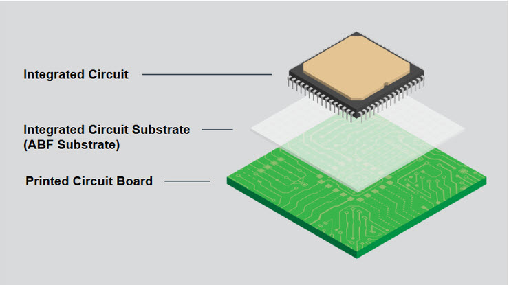
In the package stack, the ABF substrate sits directly under the silicon die, redistributing thousands of die-level connections to the BGA ball array, and the BGA in turn solders to the host PCB. The substrate carries three jobs at once: fine-pitch electrical redistribution, a stable mechanical platform matched to silicon, and a thermal path away from the die.
How ABF Build-Up Film Technology Works
The defining feature of the technology is sequential build-up. A rigid core — often a BT-class or similar laminate — carries the coarser inner layers, then ABF film layers are added alternately with thin copper foil. Each cycle is: laminate the film, laser-ablate or photo-define the microvia openings, desmear, plate copper, pattern the fine lines photolithographically, and repeat. Processor-class packages commonly stack ten or more of these layers, which is far beyond what glass-cloth build-up can achieve economically at the same geometry.
Because the film is photo-imageable, via formation does not depend on drilling. That removes the mechanical limits of drill bits and the filling problems of small drilled holes, and it lets via diameters and pad sizes shrink together with the lines. The result is an interconnect density that no drilled glass-cloth construction matches — the core reason the entire high-performance computing industry standardized on this film in the 1990s and never left it.
The same properties that make the film patternable make it demanding to process: it is unfilled by glass cloth, so the stack’s mechanical strength comes from the core and the copper, and the film layers must be handled with semiconductor-grade cleanliness. This is a large part of why ABF substrate capacity is capital-intensive and why the qualified-supplier list for the film itself is famously short.
Why ABF Enables Fine-Line, High-Pin-Count Packaging
The numbers tell the story. Volume ABF substrates pattern lines and spaces in the 10 µm class and below, while BT-class glass-cloth substrates work in a 25–80 µm window and conventional multilayer PCBs sit around 3 mil (75 µm) with advanced HDI reaching roughly 2/2 mil (about 50 µm). A modern processor die presents thousands of connections at pitches that simply cannot escape through coarser geometry — the substrate is where that density gets solved.
Dielectric performance matters as much as geometry. ABF film keeps dielectric loss low enough that multi-gigahertz die-to-ball transitions stay within budget, and its low thermal expansion matches the silicon above it, protecting the enormous number of micro-solder joints a flip-chip die makes. Add the smooth surface that permits very thin, very even copper layers, and the film covers every requirement a high-pin-count package has.
| Attribute | ABF substrate | BT substrate | Conventional FR-4 PCB |
|---|---|---|---|
| Line/space capability | 10 µm class and below | 25–80 µm typical | ≈75 µm conventional; ≈50 µm (2/2 mil) advanced HDI |
| Build-up dielectric | Photo-imageable ABF film, sequential layers | Glass-cloth BT prepreg | Glass-cloth epoxy prepreg |
| Typical package layer count | 10+ for processors | Moderate builds | Not a package — board level |
| Tg | High, film-dependent | 170–220 °C | 130–160 °C standard grades |
| Relative material cost | ≈ 1.5–2× BT | Baseline for IC substrates | Lowest |
| Representative users | CPU, GPU, FPGA, ASIC (FC-BGA) | Memory, RF, MEMS packages | Host boards and backplanes |
Read the table as a boundary map. If your chip’s package datasheet says FC-BGA with ABF build-up, the substrate decision has been made upstream at a level of capability no PCB quotation can substitute for. Your leverage as a buyer is everything below the balls — and that is where the rest of this guide concentrates.
ABF Substrate vs BT Substrate: Which Class Does Your Chip Need?
For most hardware teams this question answers itself once the chip is chosen, because the package type is fixed by the silicon vendor. The question still matters for planning: ABF-based packages concentrate in CPUs, GPUs, FPGAs, AI accelerators, and high-end networking silicon, while BT-based packages cover memory, RF front-ends, and MEMS. A board that mixes both — an accelerator card with a large FPGA and DRAM beside it, for example — carries both classes of package and inherits both sets of board-level constraints.
The cost difference between the classes is real but belongs to the chip vendor, not to your board BOM. What does land in your project is schedule and risk: ABF substrates sit at the end of a supply chain famous for capacity constraints, and package lead times propagate directly into your build plan. A practical rule is to treat ABF-packaged silicon as long-lead material and BT-packaged silicon as comparatively flexible, then plan procurement buffers accordingly.
If you want the volume-class counterpart in detail, our BT substrate guide covers its properties, manufacturing flow, and applications. Between the two articles you can place any organic package substrate you encounter on the density-versus-cost curve and know what it implies for the board underneath.
Where ABF Substrates Are Used
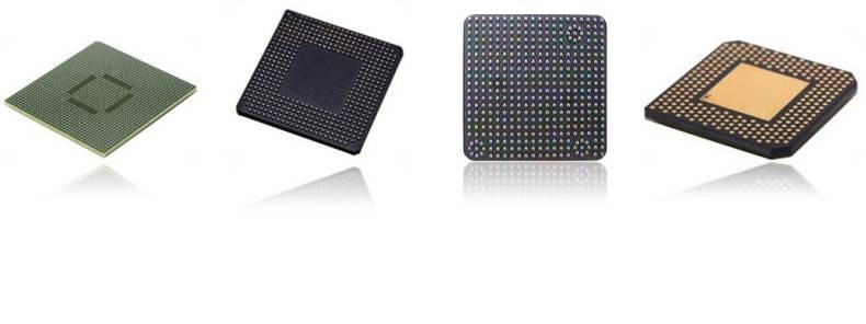
AI training and inference accelerators are the most visible users today: their dies present thousands of power and signal connections, and the ABF substrate is the only organic platform that escapes that density while carrying hundreds of watts. Servers and workstations follow the same pattern for CPUs, and high-end FPGAs and ASICs use the same packaging class when their I/O counts outrun glass-cloth substrates.
Networking and data-center infrastructure are quieter but equally dependent. Switch fabrics, optical-module DSPs, and high-speed PHYs all push signal integrity requirements that favor fine-line, low-loss substrates — and the modules that carry those signals eventually land on boards like an optical module PCB or a high-speed backplane, where the package’s work must continue without interruption.
| Segment | Representative chips | Why ABF fits |
|---|---|---|
| AI accelerators | Training and inference processors | Thousands of die connections plus high power delivery |
| CPUs and servers | Multi-core processors | Very high pin counts in large FC-BGA arrays |
| Networking | Switch fabric, PHY, optical DSP | Low loss at multi-gigahertz speeds |
| FPGA and ASIC | High-I/O programmable and custom logic | Fine geometry escapes dense die bump fields |
| Advanced driver compute | In-vehicle high-performance processors | Density plus reliability under thermal cycling |
ABF Substrate Supply and Qualification Basics
Two structural facts shape ABF substrate supply. First, the dielectric film itself comes from a very small number of qualified producers, and substrate fabricators cluster around a handful of large manufacturers with semiconductor-grade capacity. Second, qualification cycles are long: a substrate design, its film stack, and its factory are qualified together, and re-qualification after any change can take months. Both facts reward buyers who plan silicon orders far ahead and punish teams who discover substrate lead times inside their build schedule.
For procurement, the practical playbook is modest: identify which packages in your BOM are ABF-class, treat them as long-lead items with explicit buffers, and keep a second-source conversation open at the chip-vendor level even if you never exercise it. None of this requires substrate expertise — it requires recognizing that the package, not the board, is the schedule bottleneck.
From ABF Package to Host PCB: What Designers Own
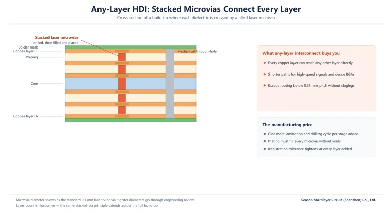
Everything below the BGA balls is yours, and an ABF package raises the stakes on all of it. The breakout region under a large FC-BGA is the densest copper on the whole board; microvias, stacked or staggered, are usually mandatory, and the via strategy must be fixed before stackup design, not after. Power delivery is the second item: a package that draws hundreds of watts expects the board to feed it through well-planned planes and via farms, not through a trace graveyard.
Signal integrity comes third and is the least forgiving. The substrate finishes its impedance and loss budget at the ball; the board must continue it through pad geometry, layer transitions, and dielectric choice. This is where HDI capability and controlled-impedance manufacturing stop being optional — our HDI PCB technology overview and the computing boards we build, such as a 14-layer computing PCB, exist precisely for this class of design.
| Package trait | What it asks from the host PCB |
|---|---|
| Very fine ball pitch | Laser microvia breakout, controlled pad geometry, tight registration |
| High power draw | Solid planes, substantial copper weight, via stitching for current and heat |
| Multi-gigahertz interfaces | Low-loss dielectric, impedance tolerances stated and verified |
| Large body size | Flatness planning, stiffness, and reflow-support considerations |
| Long substrate lead time | Early board-data freeze so layout never becomes the bottleneck |
What Comes After ABF: Glass Substrates and Next-Generation Options
ABF substrates are the incumbent, not the end state. Glass-core substrates have attracted serious investment because glass offers exceptional flatness, dimensional stability, and the prospect of even finer geometry at panel scale, and early generations are working their way through qualification for future high-density packages. Chiplet-style advanced packaging adds another direction: instead of one enormous die on one enormous substrate, multiple smaller dies are integrated on an interposer or enhanced substrate, changing how density is achieved but not removing the need for it.
For buyers the near-term conclusion is stability: ABF-class packaging will dominate high-performance computing for years, and glass adoption will arrive first inside chip vendors’ own package roadmaps rather than as a board-level choice. Our glass substrate overview covers the emerging technology in its own right, including what it does and does not change at board level.
How to Prepare Your Board for ABF-Packaged Chips
Preparation is mostly sequencing. Fix the package footprint, ball map, and breakout strategy before stackup design; set impedance targets for every interface leaving the package while the stackup is still fluid; and freeze board data early enough that a substrate lead-time surprise never stacks on top of a layout slip. The checklist below covers the items teams most often leave too late.
- Pull the package drawing and substrate overview from the chip vendor and record pin-1 orientation, ball pitch, and body size in the footprint library.
- Choose the via technology for the breakout region — laser microvia count, stack or stagger — and confirm it against your fabricator’s HDI capability.
- State impedance and loss budgets per interface, with tolerances, and have the stackup engineered against them.
- Plan power delivery: plane assignments, via farms, and decoupling placement sized for the package’s real current draw.
- Verify the board surface finish and pad geometry against the package balls’ assembly requirements.
- Agree the IPC acceptance class and inspection expectations before quoting, then hold both the substrate datasheet and board spec in the same design review.
Run that sequence and the ABF package becomes just another component with sharp edges — demanding, but fully plannable. Skip it and the same package becomes a late-stage redesign with a silicon lead time attached.
Frequently Asked Questions
What is an ABF substrate?
An ABF substrate is an IC package substrate that uses Ajinomoto build-up film — a photo-imageable epoxy-class dielectric — as its insulating layers. It is the standard platform for FC-BGA packages on CPUs, GPUs, FPGAs, and AI accelerators, supporting line/space in the 10 µm class and below and package layer counts of ten or more.
What is Ajinomoto build-up film made of?
It is a filled epoxy-resin film, originally developed from amino-acid byproduct chemistry, engineered for very high insulation resistance, low thermal expansion, and an exceptionally smooth surface. The smoothness is what allows ultra-fine copper lines to be patterned directly on it, and the photosensitive formulation lets via holes be defined photolithographically instead of drilled.
ABF or BT substrate — which one does my chip need?
The chip vendor decides, and the package datasheet states it. ABF substrates carry processor-class FC-BGA packages — CPUs, GPUs, FPGAs, AI accelerators — where thousands of connections need sub-10 µm geometry. BT substrates carry memory, RF, and MEMS packages where 25–80 µm line/space is sufficient at lower cost. A board can and often does mix both package classes.
Why are ABF substrates more expensive than BT substrates?
Three reasons compound: the dielectric film itself is a specialty material in short supply, the sequential build-up process runs many more layers with photolithographic precision, and qualification requirements approach semiconductor-fab standards. The net effect is a material-cost position of roughly 1.5–2 times BT-class substrates, before the added processing cost is counted.
Can standard PCB manufacturers produce ABF substrates?
No. Package substrate manufacturing is a separate, semiconductor-grade business with its own qualification regime, and the film supply itself is tightly concentrated. What a strong PCB partner provides is the host board for the ABF-packaged chip: HDI breakout, controlled impedance, low-loss materials, and power delivery engineered to continue what the substrate started.
Does an ABF package change how I design the host PCB?
Yes, materially. Fine ball pitch forces a laser-microvia breakout strategy chosen before stackup design. High power draw demands deliberate plane, copper-weight, and via-stitching planning. Multi-gigahertz interfaces require impedance tolerances stated and verified, not assumed. Treat the package drawing and substrate datasheet as board-level inputs from day one.
Is ABF substrate supply risky, and how should buyers plan for it?
The supply base for both the film and the finished substrates is concentrated among a small number of qualified producers, and re-qualification cycles are long, so capacity tightness translates quickly into package lead times. Practical planning: identify ABF-class packages in your BOM, treat them as long-lead items with explicit buffers, and keep a second-source conversation open with the chip vendor.
Building the Board Under an ABF-Packaged Chip?
High-pin-count packages put the burden on your stackup, breakout region, and power delivery — exactly the work our engineering team does daily. Our PCB manufacturing services cover HDI microvias, controlled impedance, and low-loss materials for processor-class designs. Send your Gerber data for an engineering review, or start with our PCB materials and laminates guide to set the stackup on the right footing.