Book Appointment Now

A buyer-side guide to glass substrate PCBs: CTE and loss advantages, TGV processing, honest comparison with FR-4 and HDI builds, and where glass fits today.
Glass Substrate PCB Explained: Properties, TGV and Where It Fits
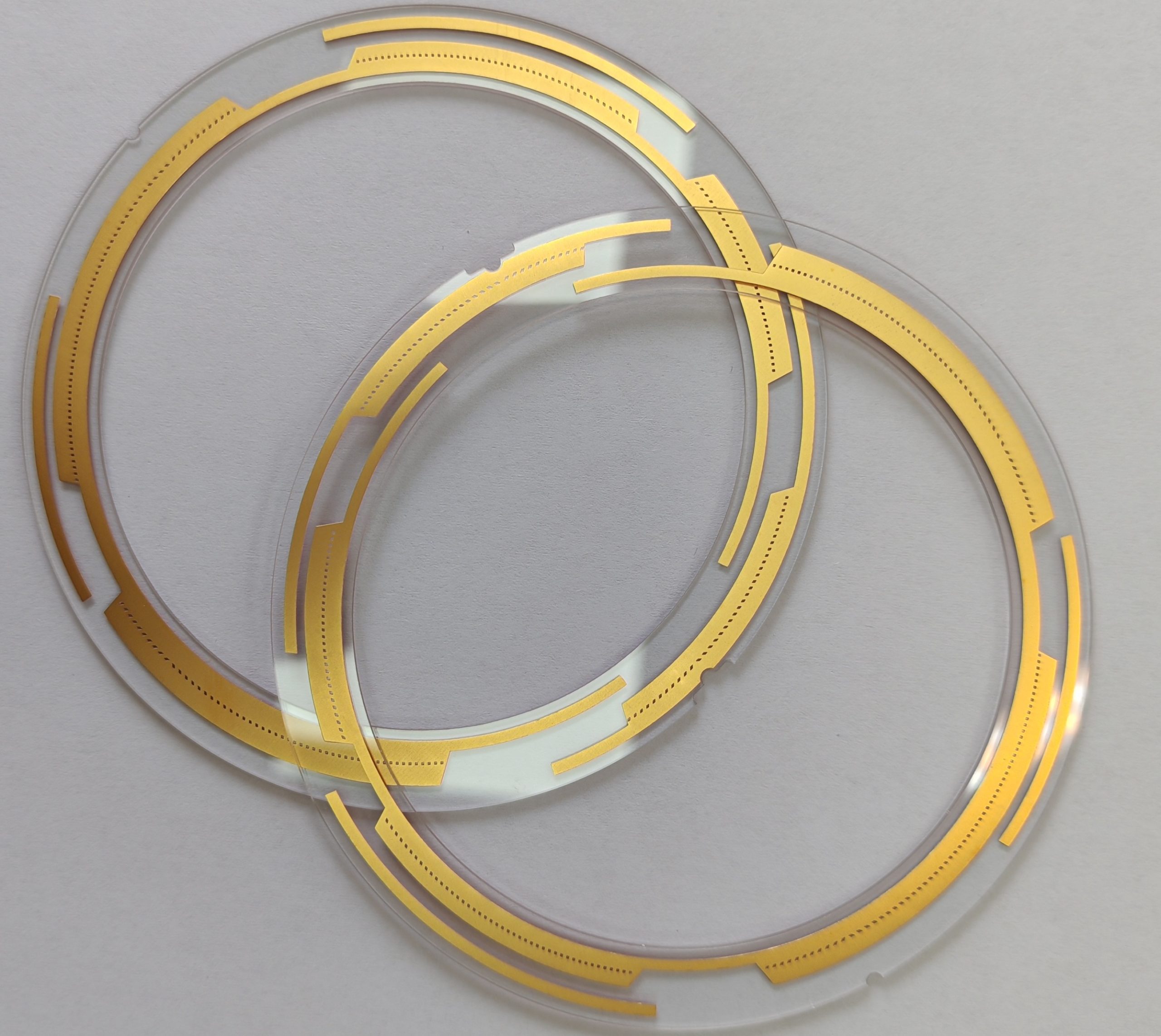
Every few years a material story reshapes the packaging conversation, and glass is the current one. A glass substrate PCB replaces the organic composite core at the heart of a board or an IC package with an engineered glass panel — thermally matched to silicon, flat to sub-micrometer roughness, and stable at frequencies where organic materials start to lose signal. The technology is real and advancing quickly, but so is the marketing surrounding it.
This guide separates the two. It covers what glass genuinely changes — coefficient of thermal expansion, dielectric behavior, dimensional stability — how through-glass vias are formed, and where glass already outperforms organic substrates. Just as importantly, it draws the honest boundary: which parts of the story a conventional PCB fabricator participates in today, and which remain the territory of semiconductor-style packaging lines.
Table of Contents
- What Is a Glass Substrate PCB?
- Why Glass Cores Entered the Conversation
- Glass Core vs FR-4 vs High-Speed Organic Laminates
- TGV: How Vias Are Formed in Glass
- Where Glass Substrates Pay Off — and Where They Do Not
- What a Conventional PCB Fabricator Can and Cannot Build Today
- Glass Substrate PCB Cost and Supply Reality
- A Buyer’s Checklist Before Specifying Glass
- FAQ
- Close the Gap With an Organic Build Today
What Is a Glass Substrate PCB?
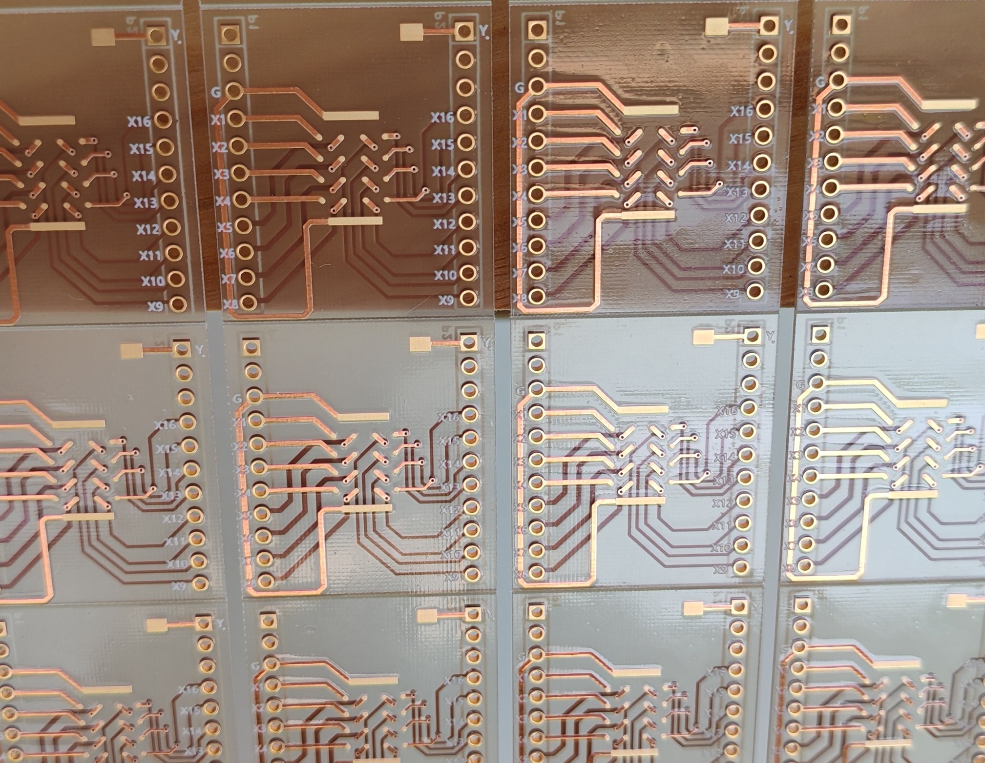
A glass substrate PCB is a circuit board whose core dielectric is a monolithic glass panel — typically a borosilicate or fused-silica glass — rather than an organic composite. Copper interconnect layers are formed on the glass surfaces and, in advanced builds, inside through-glass vias that connect the two sides. The concept appears in two settings: as the package substrate that carries a chip or chiplet directly, and as board-level panels where fine interconnect density is required beyond what organic laminates resolve economically.
A common confusion is worth clearing up immediately. FR-4 already contains glass — woven glass cloth reinforcing the epoxy resin — but that is reinforcement, not a glass core. In a true glass substrate, the load-bearing dielectric itself is glass: a brittle, dimensionally exact panel that behaves optically, thermally and electrically in ways no woven composite can. The distinction matters because datasheets and articles sometimes blur the two, and a buyer who specifies one while thinking of the other will be disappointed either way.
Why Glass Cores Entered the Conversation
The first driver is thermal. Silicon expands at roughly 2.6 ppm/°C; engineered glass formulations can be tuned into the 3–10 ppm/°C range, while organic laminates run at roughly 12–17 ppm/°C. On a large package — the kind AI accelerators use — that difference accumulates into real warpage during reflow and thermal cycling, and warpage is one of the top yield killers in advanced packaging. A core that moves with the silicon instead of against it removes a whole failure class.
The second driver is flatness. Glass panels reach surface roughness around Rz 1 µm as manufactured, which is smooth enough for fine-line photolithography — features in the low single-digit micrometers — to be patterned directly on the panel. Organic laminates, by contrast, carry a copper profile engineered for adhesion, and every micrometer of that roughness becomes dielectric loss at high frequency. Dimensional stability completes the set: glass barely moves with temperature and humidity, so registration between layers holds even on large panels.
None of these properties is new — glass has been the interposer material of research literature for over a decade. What changed is that interconnect density and package sizes have grown to the point where the organic route is straining, which moved the industry conversation from laboratories to roadmaps. Industry bodies, including the IPC standards organization, now have working groups documenting test methods and design guidance for glass-based substrates — a sign of a technology moving from experiment to supply chain.
Glass Core vs FR-4 vs High-Speed Organic Laminates
The honest comparison is a three-way one. Glass cores compete on thermal match, flatness and stability; FR-4 competes on cost, toughness and decades of manufacturing maturity; high-speed organic laminates — PTFE-based, hydrocarbon, or low-loss resin systems — compete on proven low-loss performance at mmWave frequencies. The table below summarizes representative ranges; specific glass compositions vary, so treat them as orientation rather than datasheet values.
| Property | Glass core | FR-4 | High-speed organic laminate |
|---|---|---|---|
| CTE (ppm/°C) | 3–10, tunable by composition | 12–17 | 10–20 depending on resin system |
| Dielectric constant (GHz range) | ≈3.8–5.5 by glass type; very stable | 4.2–4.7 | 3.0–3.7 |
| Loss tangent (GHz range) | Very low, composition-dependent | 0.015–0.025 | 0.001–0.005 |
| Thermal conductivity (W/m·K) | ≈1.0–1.5 | 0.3–0.5 | 0.4–0.8 |
| As-manufactured surface roughness | Rz ≈1 µm, lithography-ready | Roughened copper profile for adhesion | Roughened copper profile for adhesion |
| Finest practical line/space | Low single-digit µm with lithography | 50–100 µm (2–4 mil class) | 75–150 µm typical |
| Manufacturing maturity | Emerging; package-substrate volumes | Decades, fully mature | Mature, widely available |
Read the table as three different centers of gravity rather than a ranking. Glass wins the properties that matter at the package level — thermal match, flatness, interconnect density — while organic laminates win everything that matters at the board level: cost, impact toughness, panel size, repairability and an enormous qualified supplier base. The loss tangent row deserves a caveat: at mmWave frequencies, glass can be excellent, but well-chosen organic high-frequency laminates are already excellent too, and they arrive through channels every PCB buyer can access today.
TGV: How Vias Are Formed in Glass
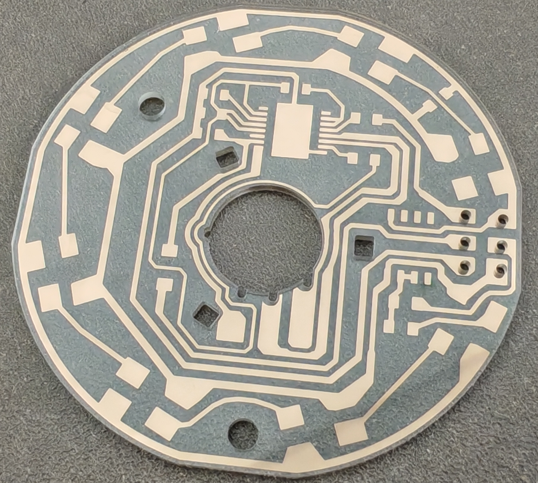
The enabling process for glass interconnect is the through-glass via, TGV. Instead of mechanical drilling, the glass is locally modified by a laser and the modified volume is selectively etched away, leaving clean microvials through the panel with diameters in the tens of micrometers and aspect ratios well beyond what mechanical drilling achieves in organic material. Metallization follows semiconductor practice: a seed layer is deposited across the panel and the vias are filled or lined by electroless and electrolytic copper, producing vertical interconnect with geometry organic processes cannot reach.
The contrast with conventional HDI is instructive. On organic builds, laser microvias at 0.1 mm diameter — 0.076 mm on engineering review — and mechanical drills form the vertical connections, stacked and staggered across 1-Stage, 2-Stage and 3-Stage build-ups as described in our HDI stages guide. Glass TGV pushes density and aspect ratio well past those numbers, but it does so with laser-and-etch equipment and handling discipline closer to a semiconductor line than a PCB drill room. Same goal, different industrial world — which is exactly why the two supply chains have stayed separate.
Where Glass Substrates Pay Off — and Where They Do Not
Application fit decides everything, and the fit map is clearer than most coverage suggests. Glass earns its premium where silicon is close, interconnect is dense, or frequency is extreme. It struggles where boards must be large, tough, inexpensive, or produced in enormous volume — which is most of the PCB market.
| Application | Why glass helps | Practical alternative today |
|---|---|---|
| AI/HPC package substrates | CTE match cuts warpage on very large packages; dense TGV fanout | Organic package substrates — qualified, scaling |
| mmWave antennas and front ends | Stable dielectric constant and low loss across temperature | PTFE and hydrocarbon high-frequency laminates |
| Optical and electro-optical modules | Transparent, dimensionally exact, lithography-ready surface | Conventional rigid builds with precise registration |
| MEMS and sensor carriers | Flatness and stability protect sensitive structures | Standard FR-4 with careful stackup design |
| Consumer and industrial boards | Rarely justified — cost and toughness favor organics | FR-4 and HDI organic builds |
The pattern to remember: glass substitutes for organic package substrates before it substitutes for PCBs. The volumes and economics of board-level glass — a full multilayer circuit board on a glass core — are further out than the packaging story, and coverage that treats the two as the same milestone confuses the timeline.
One more selection trap deserves its own paragraph. When a glass substrate PCB is proposed for a board-level design, the specification usually smuggles in a package-level assumption — that the interconnect will be lithography-defined and the core will hold exact registration. On an organic board the same densities are reached with HDI microvias instead, and the design rules that govern them are different in kind, not just in number. Translating the requirement into the constraint that actually matters — pitch, fanout region, impedance class — keeps the conversation with either supply chain honest and the quote comparable.
What a Conventional PCB Fabricator Can and Cannot Build Today
Honesty helps both sides here, so let us be specific. Glass-core substrates are manufactured on semiconductor-style lines: photolithography, laser modification and etch, panel-level metallization. That equipment does not exist on a conventional PCB fabrication floor, and a PCB fabricator that claims production glass capability today deserves a very close look at its supply chain — the credible answers involve packaging partners, not in-house glass lines.
What a capable PCB fabricator does offer is the organic route to the same signal-integrity goals. High-frequency builds on low-loss laminates — see our double-sided Rogers high-frequency PCB as a released example — carry mmWave designs today. Dense interconnect comes from HDI: our 10-layer 2-stage HDI prototype shows stacked microvias and fine-line fanout in production form, and our 6-layer optical module PCB carries 100G/400G-class transceiver designs on conventional organic materials.
The practical advice for most design teams: when a glass substrate promises a solution to a warpage, density or loss problem, first check how far a well-executed organic build closes the same gap. Our PCB materials and laminates guide and the laminate selection guide cover that decision space — and in a majority of current designs, the organic answer is sufficient at a fraction of the supply-chain risk.
Glass Substrate PCB Cost and Supply Reality
Glass is not yet a price-competitive material, and the reasons are structural. Panel handling is the first challenge — glass is brittle, and every cutting, transport and processing step manages microcrack risk that organic laminates simply do not have. Via metallization yield is the second: filling tens-of-micrometer vias uniformly across a large panel is a semiconductor-grade yield problem. The result is that a glass core today carries a substantial multiple of an organic package substrate’s cost, before the interconnect on top of it is counted.
The trajectory matters more than the current number. Investment across the advanced packaging ecosystem is scaling panel sizes, improving via yields and building the second-source landscape that real production requires. For buyers, the sensible posture is staged: track glass for next-generation package-level needs, qualify it through packaging channels rather than PCB channels, and keep organic alternatives design-current so a supply hiccup never strands a program. Cost gaps in emerging materials close faster than requalification timelines, and the programs that navigate the transition are the ones that kept both options alive — watching the standardization work of the Global Electronics Association as it matures.
A Buyer’s Checklist Before Specifying Glass
- Quantify the problem glass would solve: is it CTE-driven warpage, interconnect density, or loss? If the answer is vague, the material choice is premature.
- Check the organic alternative honestly: a low-loss laminate with a disciplined HDI stackup closes most current design gaps.
- Source through the right channel: glass cores come from advanced packaging suppliers, not standard PCB fabrication quotes.
- Demand reliability data on your geometry: thermal cycling and microcrack behavior are glass-specific risks that generic datasheets will not answer.
- Confirm second-source and requalification paths before committing a program timeline to a single line.
- Match volume to maturity: prototype quantities through packaging channels are realistic; high-volume board-level glass is not yet a commodity.
Run the list in order and the glass decision usually resolves itself: the problems glass uniquely solves appear at the package level, while most board-level needs remain the organic laminate’s home ground. The checklist also doubles as a filter for supplier conversations — anyone pitching glass capability should clear all six points without hedging.
Frequently Asked Questions
What is a glass substrate PCB?
It is a circuit board or package substrate whose core dielectric is a monolithic glass panel — typically borosilicate or fused silica — instead of an organic composite. Copper interconnect is formed on the glass surfaces and through through-glass vias, offering thermal expansion matched to silicon, near-optical flatness and stable electrical performance at high frequency.
Is FR-4 a glass substrate?
No, although it contains glass. FR-4 is an epoxy resin reinforced with woven glass cloth — the glass strengthens the composite but the dielectric is still an organic resin system. In a true glass substrate PCB, the load-bearing core itself is engineered glass, which is a fundamentally different material with different processing and different failure modes.
What is a TGV (through-glass via)?
A TGV is a microvia formed through a glass panel by laser modification followed by selective etching, then metallized with a seed layer and copper. Diameters sit in the tens of micrometers with aspect ratios well beyond mechanical drilling, which is what enables the dense vertical interconnect that makes glass substrates attractive for advanced packaging.
What advantages does glass offer over organic laminates?
Three headline properties: thermal expansion tunable down to 3–10 ppm/°C, closely matching silicon and cutting warpage on large packages; as-manufactured surface roughness near Rz 1 µm, fine enough for lithography-defined features; and dimensional stability with temperature and humidity, which holds layer-to-layer registration on large, dense panels.
Why are glass substrate PCBs not common yet?
Three barriers dominate: brittleness, which makes every handling and cutting step a microcrack risk; cost, with glass cores still carrying a substantial multiple of organic substrate pricing; and an immature ecosystem — panel sizes, second sources and standard test methods are still being established. Packaging-level use is scaling first; board-level glass follows later.
Can I prototype a glass substrate board today?
Prototypes are realistic through advanced packaging channels, not through conventional PCB fabrication quotes, because the lithography and TGV equipment lives on semiconductor-style lines. For most design problems that glass is proposed to solve, a well-executed organic build — low-loss laminate plus HDI stackup — is available now from standard fabrication channels at lower supply-chain risk.
How do I choose between glass, FR-4 and high-speed laminates?
Start from the binding constraint. Warpage on very large silicon? Glass wins. mmWave loss within a normal board outline? Qualified high-frequency organic laminates usually suffice. Cost-sensitive volume production? FR-4 and HDI remain the rational default. When the constraint points to glass, source through packaging suppliers and validate reliability on your own geometry before committing.
Close the Gap With an Organic Build Today
If glass substrates entered your roadmap for warpage, density or signal-loss reasons, send us the design and the constraint. Our engineering review evaluates how far a disciplined HDI stackup with a low-loss laminate closes the same gap, and returns a stackup proposal with the impedance and feature-size numbers you can hold us to.
Start through our PCB manufacturing services page — 2–30 layer prototypes and production, HDI build-ups and high-frequency laminates, with first-article evidence attached to every release.