Book Appointment Now

PCB barrel crack causes and prevention: plating thickness by IPC class, Z-axis expansion, aspect ratio limits, drill quality, and the tests that catch it.
PCB Barrel Crack: Why Plated Holes Crack and How to Prevent It
A PCB barrel crack is a fatigue fracture inside the copper wall of a plated through-hole: the board passes continuity at room temperature, then opens intermittently on the line or in the field, usually after assembly. Because the crack is hidden inside the hole, it is one of the most misdiagnosed failures in electronics. Assembly gets blamed first, the solder joint is reworked, and the real defect stays in the barrel.
This guide explains where the crack starts in cross section, why Z-axis expansion loads the copper every thermal cycle, which specification lines actually control the risk, plating thickness by IPC class, aspect ratio, drill and desmear quality, and the tests that expose a weak barrel before it ships. The aim is practical: by the end, you should be able to read a fab drawing and a cross-section report and know whether the barrel was ever going to survive.
Table of Contents
- What a PCB Barrel Crack Looks Like in Cross Section
- Why the Barrel Is Loaded: Laminate Expansion Against Copper
- Plating Thickness Is the First Gate
- Drilling and Desmear Decide Whether the Wall Bonds
- How Aspect Ratio Raises PCB Barrel Crack Risk
- Design Choices That Pre-Load the Barrel
- Detecting a PCB Barrel Crack Before It Ships
- Failure Location, Root Cause and Countermeasure in One Table
- Prevention Checklist, Stage by Stage
- What a Barrel Crack Costs in Schedule
- Questions That Separate a Real Answer From a Brochure
- FAQ
- Have the Barrel Margin Reviewed Before You Order
What a PCB Barrel Crack Looks Like in Cross Section
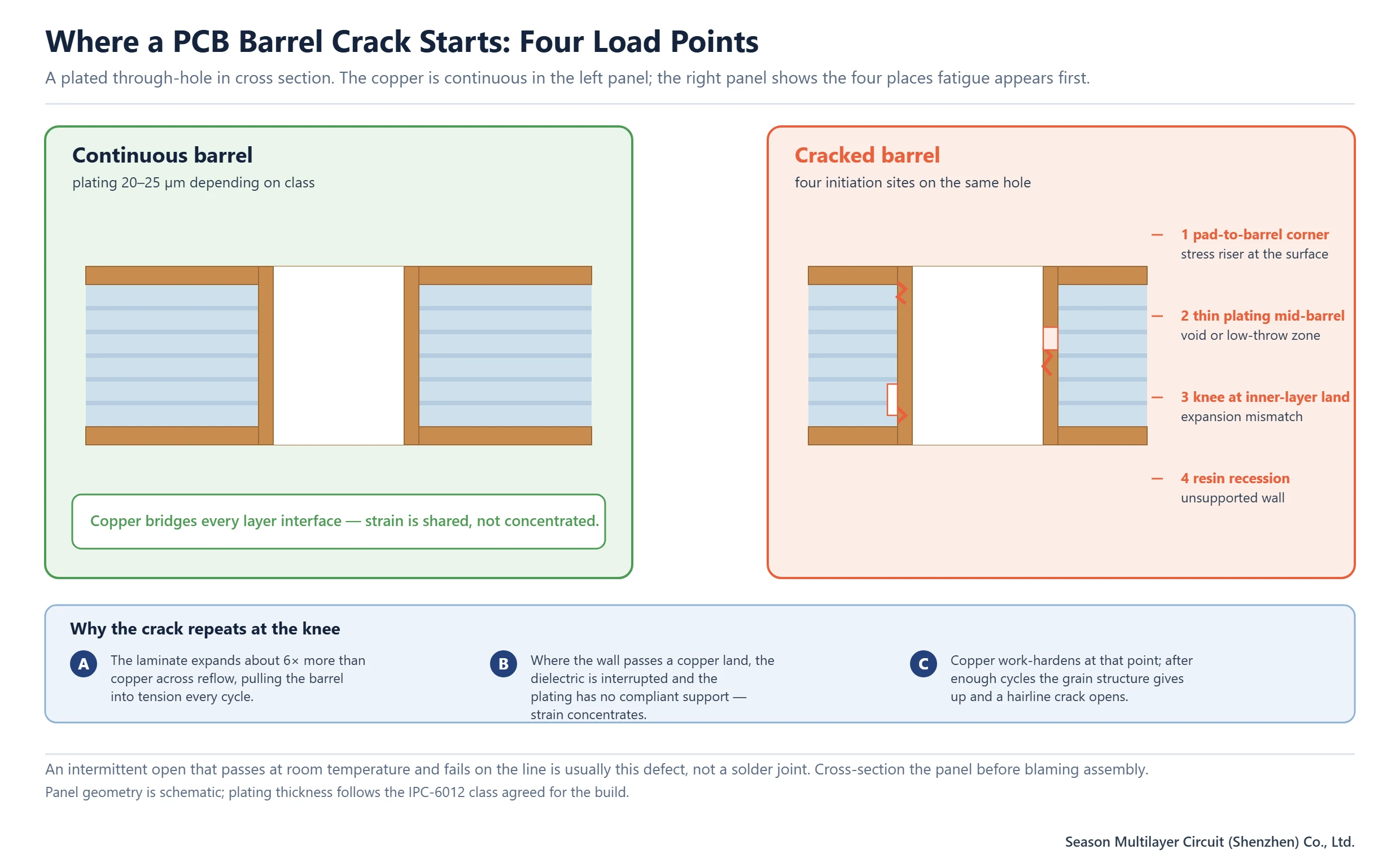
In a cross-section photograph the crack is rarely dramatic. It is a hairline separation in the plated copper, most often at one of four places: the corner where the barrel meets the surface pad, the knee where the wall passes an inner-layer land, a mid-barrel zone where plating ran thin or a void formed, and a length of wall left unsupported by resin recession. The rest of the barrel looks perfectly normal, which is exactly why low-magnification inspection misses it.
The electrical signature matches the geometry. A crack that is still closed reads as a slightly elevated or drifting resistance; once it opens, the connection becomes intermittent, and the failure reproduces only under temperature or flexure. A board that tests fine on the bench at 23 °C and fails during reflow, burn-in or thermal cycling is showing the classic pattern, and no amount of solder-joint rework will fix a PCB barrel crack.
Location also carries information about cause. A corner crack points at pad-side stress and plating geometry; a mid-barrel crack points at plating thickness or a void; a crack at every knee points at expansion mismatch against thick laminate. Reading the location before the root cause saves a full round of speculation, and it is the first thing to record when a PCB barrel crack is found.
Why the Barrel Is Loaded: Laminate Expansion Against Copper
The mechanism is a mismatch of thermal expansion in the Z-axis. Copper expands at roughly 17 ppm/°C. An FR-4 laminate expands at 40–55 ppm/°C below its glass transition and at 200–300 ppm/°C above it, and a lead-free reflow peak of 245–260 °C pushes every board through that transition. Over one excursion a typical laminate grows about 2.3–4.0% in thickness while the copper inside it grows about 0.4%.
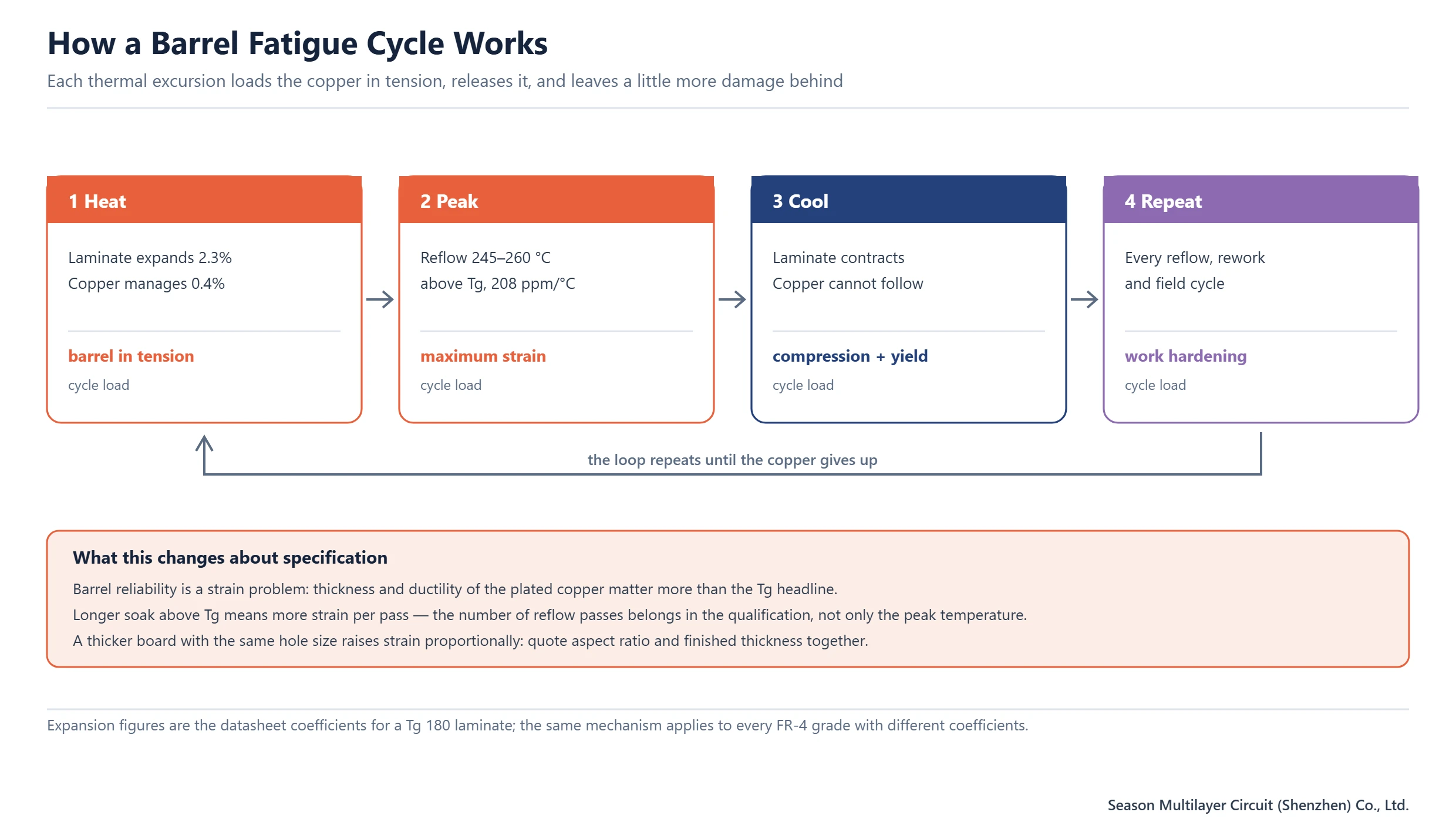
The difference has to go somewhere. The plated barrel is bonded to the laminate at both ends, so the laminate’s extra growth stretches the copper in tension at every peak and compresses it on the way down. Copper can absorb that elastically only a few tenths of a percent; beyond that it yields, and repeated yielding work-hardens the metal until a hairline forms. Every reflow pass, rework cycle and field thermal cycle adds to the count.
Two consequences follow for specification. First, thicker boards put more absolute strain into the same barrel, so finished thickness and hole size belong in the same sentence. Second, the number of thermal passes matters as much as the peak: a board built for three reflow passes and no rework lives an easier life than the same stackup sent through five. Both belong in the qualification conversation, not just the peak temperature on the profile.
Plating Thickness Is the First Gate
Copper in the barrel is the material that carries the strain, so its thickness is the single most effective lever. IPC-6012 sets the minimums by performance class, and the numbers are not interchangeable: Class 3 products are simply built with more copper in the hole than Class 2 products, and a drawing that leaves the class unspecified leaves the plating thickness unspecified with it. See the IPC standards overview for how the class system is structured.
| Performance class | Copper in barrel, average | Copper in barrel, minimum | Typical use |
|---|---|---|---|
| IPC-6012 Class 1 | defined by drawing | defined by drawing | Consumer electronics where function only is required |
| IPC-6012 Class 2 | 20 µm | 18 µm | Standard commercial and industrial products |
| IPC-6012 Class 3 | 25 µm | 20 µm | High-reliability products and long-life equipment |
| High-aspect-ratio build | per engineering review | per engineering review | Thick boards above roughly 10:1, confirmed by coupon |
Average and minimum are different numbers, and the gap between them is where cracks are born. A barrel that averages 25 µm but thins to 12 µm at one knee has a weak point, not a robust plating. The microsection that proves compliance should be taken from a coupon that went through the full plating cycle with the production panel, and the thinnest reading, not the average, is the number that predicts life. When a PCB barrel crack shows up, the plating coupon and the drill log are the first two documents to pull, because thickness is the first gate.
Drilling and Desmear Decide Whether the Wall Bonds
Plating can only be as good as the wall it grows on. A worn drill bit smears resin over the glass fibres and tears the wall; that smear is a barrier the electroless copper cannot bridge, and the plated deposit above it is discontinuous. Bit hit counts, in-feed and spindle condition are therefore barrel-quality controls, not just drilling productivity metrics, and a fabricator who cannot produce a drill log is asking for trouble on a thick board.
Desmear is the step that cleans the wall before plating, and it has a window rather than a dial setting. Under-treated walls keep smear and leave poor adhesion; over-treated walls etch the glass and leave loose fibres that seed voids. Both ends of the window end the same way, with thin or voided copper in the barrel, so process control records matter more here than on almost any other step. The chemistry route itself is covered in our hole metallization guide.
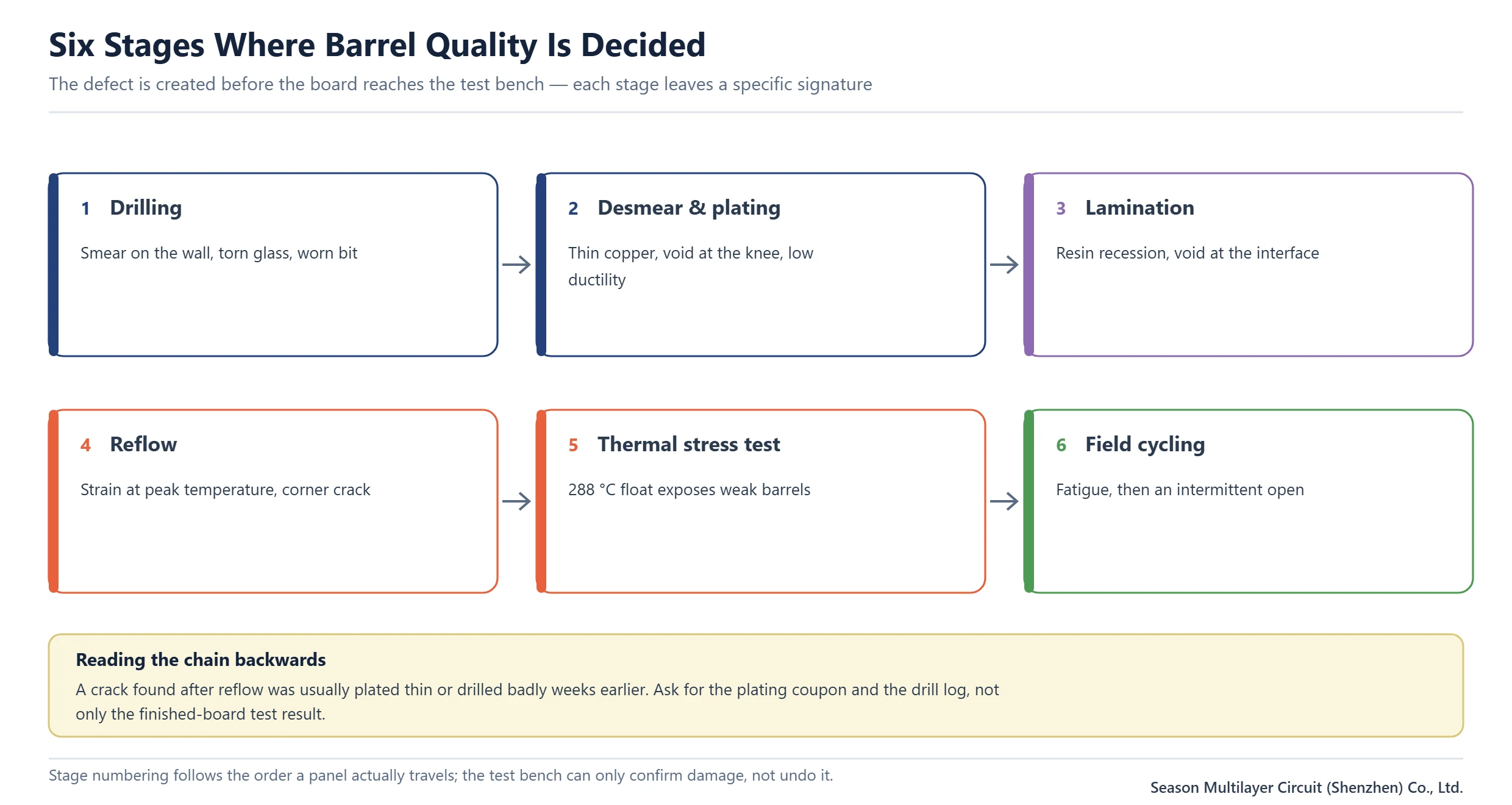
The plating bath adds its own variables. Current density distribution decides whether copper deposits evenly down a deep hole or plates heavy at the mouths and thin in the middle, which is the low-throw zone that mid-barrel cracks love. Bath analysis records, throwing-power coupons and panel-level current settings are the paperwork that separates a controlled process from a hopeful one.
How Aspect Ratio Raises PCB Barrel Crack Risk
Aspect ratio is finished board thickness divided by finished hole diameter, and it concentrates the entire expansion problem into a narrower tube. At 4:1 the plating bath throws copper evenly and the barrel shares strain comfortably. As the ratio climbs, the middle of the hole plates thinner, the drill wanders more, and every micron of laminate growth loads a smaller copper section. Past roughly 10:1 the PCB barrel crack risk is no longer a rounding error unless plating thickness is increased deliberately.
Our own process limits make the boundary explicit: through-holes at 12:1 in volume production and 20:1 on sample builds confirmed lot by lot, with blind microvias held at 1:1. The full table, including the worked examples, is maintained on the aspect ratio and plating limits page. A design that sits above the production limit is not automatically rejected, but it changes from a quoting exercise into an engineering review, and that review should happen before the order, not after the first lot fails.
| Board thickness | Drill diameter | Aspect ratio | Verdict |
|---|---|---|---|
| 1.6 mm | 0.40 mm | 4:1 | Comfortable in any qualified shop |
| 2.4 mm | 0.30 mm | 8:1 | Workable with controlled plating |
| 3.2 mm | 0.25 mm | 12.8:1 | Above the production limit; engineering review or sample build |
Design Choices That Pre-Load the Barrel
Not every PCB barrel crack is a process defect. Several design habits load the barrel before manufacturing even starts, and they are cheaper to fix in CAD than in the fab. Small holes in thick boards are the obvious case, but there are quieter ones: chains of vias used as stitching along a stiff edge, vias placed in the flexure zone of a connector mount, and vias directly under large components whose thermal cycle adds board bending to barrel strain.
Hole size affects more than ratio. A 0.20 mm finished hole leaves less wall area for the same strain and is more sensitive to a single void, so on a 2.4 mm board the difference between 0.20 mm and 0.25 mm drills is the difference between a review and a routine build. Where the schematic allows it, consolidating on the larger of two candidate hole sizes is free reliability.
Copper balance in the stackup matters too. A board with heavy copper on one side warps during reflow, and warp adds flexure strain on top of expansion strain at every via. Balanced constructions keep the barrel’s load predictable, which is one more reason the stackup review and the reliability conversation belong together rather than in separate departments.
Detecting a PCB Barrel Crack Before It Ships
Electrical test at room temperature cannot see a crack that is still closed, so the burden falls on stress-based methods. The workhorse is the thermal stress test: a solder float at 288 °C per IPC-TM-650 2.6.8 that pushes weak barrels past their limit in seconds. For products that live through many thermal cycles, an interconnect stress test cycles the barrel electrically until resistance rises, converting reliability into a measured number rather than a hope.
| Method | What it catches | Where it fits |
|---|---|---|
| Cross-section of a production coupon | Thin plating, voids, smear, recession, early cracks | Every qualification lot; the baseline evidence |
| Thermal stress, 288 °C solder float (IPC-TM-650 2.6.8) | Weak barrels that cannot survive one assembly pass | Per-lot process proof on thick or high-ratio builds |
| Interconnect stress test, resistance-monitored cycling (IPC-TM-650 2.6.26) | Fatigue life in cycles to a resistance threshold | Design qualification for long-life products |
| X-ray inspection | Void clusters and plating irregularities in sampled holes | Screening where cross-sectioning is destructive |
| Dye and pry after reflow | Cracks that opened during assembly | Failure analysis on returned assemblies |
The practical rule is to sample by risk, not by habit. A 1.6 mm board at 4:1 with Class 2 plating needs the routine coupon. A 3.2 mm backplane at 12:1 deserves cross-sections from more locations plus a thermal stress result per lot, because the cost of finding the crack after assembly is far higher than the cost of the extra coupon. Our own approach on high-ratio builds is described with the reliability testing matrix, and the same logic applies to any fabricator you qualify.
Failure Location, Root Cause and Countermeasure in One Table
Most investigations of a PCB barrel crack converge once the location is known. The table below maps the four common initiation sites to their dominant causes and the countermeasure that actually moves the needle, in the order a fab would apply them.
| Crack location | Dominant cause | Effective countermeasure |
|---|---|---|
| Pad-to-barrel corner | Stress riser at the surface; thin copper at the mouth transition | Corner fillet control, plating thickness at the minimum point, gentle drill entry |
| Mid-barrel | Low-throw zone, void, smear under the deposit | Bath throwing-power control, desmear window, hit-count discipline |
| Knee at inner-layer land | Maximum expansion strain where dielectric is interrupted | Reduce aspect ratio, raise plating class, verify with thermal stress coupon |
| Along unsupported wall | Resin recession leaving the plating unsupported | Lamination and desmear control, resin system matched to the stackup |
The mapping also explains why some fixes disappoint. Adding a whole extra plating class to a design whose crack is at the knee helps less than cutting the aspect ratio, because strain, not average thickness, is the driver there. Conversely, a mid-barrel crack on a 4:1 board is almost always a bath or desmear problem, and no amount of redesign will compensate for a thin deposit.
Prevention Checklist, Stage by Stage
Barrel reliability is bought one stage at a time, and each item below is verifiable in paperwork rather than in promises. A buyer can audit every line without standing at a production line.
- Design: keep through-hole aspect ratio at or below 12:1 for production, prefer the larger of two candidate hole sizes, and avoid via chains in known flexure zones.
- Stackup: balance copper distribution so the board does not add warp strain, and state finished thickness and hole size together on the drawing.
- Specification: name the IPC-6012 class, the minimum copper in the barrel at the thinnest point, and the coupon that will prove it.
- Drilling: require bit hit-count limits and a drill log referenced to the production panel.
- Desmear and plating: confirm bath analysis records and throwing-power coupons for deep holes.
- Verification: thermal stress per lot on thick or high-ratio builds, cross-section from more than one location, and a resistance-monitored cycle test for long-life products.
- Assembly: agree the reflow pass count and rework policy up front, because every pass spends barrel life.
None of these items is exotic, and that is the point. Most PCB barrel crack cases are the accumulation of small relaxations across several stages, so the checklist works as a conversation with the fabricator rather than as a demand list.
What a Barrel Crack Costs in Schedule
The direct costs are obvious; the schedule costs are worse and rarely priced. A crack discovered on a fabricated panel costs a re-fab plus the panel’s place in the queue. The same crack discovered after assembly costs the assembled units, the rework attempt, the diagnosis time and another full build cycle, and the diagnosis itself usually consumes the calendar of both the assembler and the fabricator while each proves it is not at fault.
High-aspect-ratio builds carry their own schedule logic: they are quoted and planned through engineering review, so feasibility is confirmed lot by lot rather than assumed. Building that review into the timeline is cheaper than discovering at CAM that a 14-layer computing board needs a hole redesign, which is why our process capability page publishes the limits before quotation. The same review discipline applies to thick industrial boards and to dense backplane work such as our automotive high-speed backplane build.
Questions That Separate a Real Answer From a Brochure
Any fabricator can claim excellent hole reliability. The questions below convert the claim into verifiable answers, and the quality of the response usually ends the selection debate faster than any audit visit.
- What copper-in-barrel minimum do you commit to at the thinnest point, and which coupon proves it on my construction?
- What is your aspect ratio limit for production, and what changes about the process above it?
- How do you control drill hit counts, and can I see the drill log for my panel?
- Which lots get a 288 °C thermal stress coupon, and what is the acceptance criterion?
- For my stackup, where do you expect the strain peak, and what did the last cross-section at that location show?
Answers that cite numbers, coupons and records indicate a controlled process. Answers that return to marketing language indicate that barrel reliability is being purchased blind, and the risk eventually lands on the programme, not on the brochure. When a PCB barrel crack does appear despite all of this, the failure analysis path is the same one used for every via defect we cover in the PCB defects guide.
Frequently Asked Questions
What is a PCB barrel crack?
It is a fatigue fracture inside the plated copper wall of a through-hole. The board usually passes electrical test at room temperature and then fails intermittently under thermal cycling or flexure, which is why the defect is so often misattributed to solder joints or assembly handling.
What causes the copper in a via barrel to crack?
Repeated strain from Z-axis expansion. The laminate grows two to four percent across a reflow excursion while the copper grows about 0.4 percent, so the barrel is stretched and released every cycle. Thin plating, voids, smear and high aspect ratio all reduce the margin the copper needs to absorb that load.
How much copper plating does IPC-6012 require in the barrel?
Class 2 requires an average of 20 µm with an 18 µm minimum; Class 3 raises this to 25 µm average with a 20 µm minimum. The minimum at the thinnest point matters more than the average, because a crack starts where the copper is weakest, not where it is thickest.
Why do barrel cracks appear after reflow and not before?
Reflow is the first event that pushes the board above the resin glass transition, where expansion jumps several-fold. A weak barrel may survive fabrication and even assembly, but each thermal pass adds work hardening, so the crack opens after one or more passes rather than at first exposure.
What aspect ratio is safe for plated through-holes?
Around 8:1 is comfortable for most qualified shops, 12:1 is a common production limit for thick boards, and higher ratios are handled as sample or review builds. The deeper the board relative to hole diameter, the thinner the plating tends to run mid-barrel and the higher the PCB barrel crack risk per cycle.
How is a barrel crack detected?
Cross-sectioning a production coupon is the baseline evidence, showing plating thickness, voids, smear and recession. Thermal stress at 288 °C per IPC-TM-650 2.6.8 exposes weak barrels in one pass, and a resistance-monitored interconnect stress test measures fatigue life directly. Room-temperature electrical test alone cannot see a crack that is still closed.
Can a barrel crack be repaired?
Not in any meaningful sense. The copper wall is inside the laminate and inaccessible once the board is built. The practical response to a PCB barrel crack is to contain the lot, cross-section to confirm the location, correct the process or design cause, and re-fab. Solder rework at the joint does not touch the defect.
Does a higher Tg laminate prevent barrel cracking?
It helps, because expansion above Tg is the dominant load, but it is not sufficient on its own. A Tg 180 laminate with thin or voided plating still cracks, and a well-plated Tg 140 barrel at a modest aspect ratio can outlive it. Plating thickness, aspect ratio and pass count decide the outcome together with the resin system.
Have the Barrel Margin Reviewed Before You Order
If the stackup, the finished thickness, the hole sizes and the reflow pass count are already defined, send them for review and the Season PCB engineering team will return the aspect ratio verdict, the recommended plating class and the coupon plan that proves it. Reviews happen before quotation, so a marginal barrel is caught while it is still a drawing change. See how we handle construction review, or submit Gerber data for a first pass.
Season PCB direct: Tel (+86) 18681528532 | WhatsApp +86 18681528532
E-mail: roc@season-pcb.com