Book Appointment Now

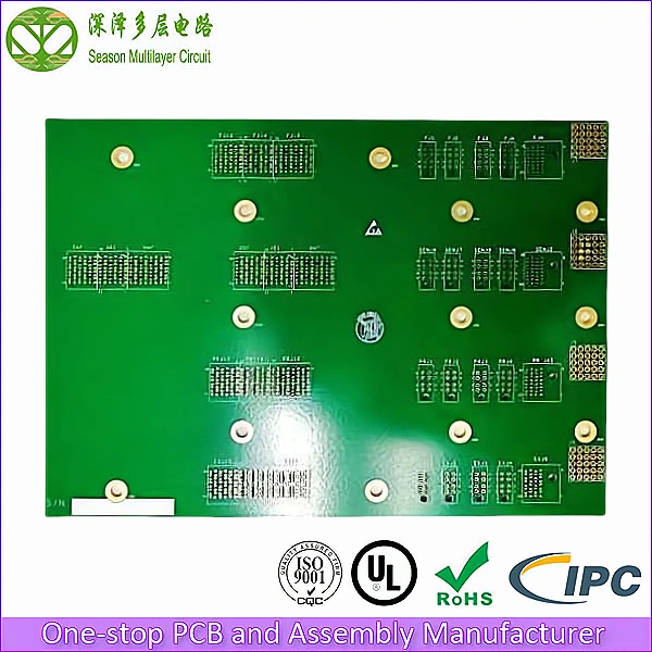
12-Layer Automotive High-Speed Backplane PCB
High-speed 12-layer backplane PCBs for automotive domain controllers, ADAS compute platforms, and central gateway modules with multi-gigabit SerDes, automotive Ethernet, and back-drilled via technology for maximum signal integrity.
Modern vehicle architectures are consolidating dozens of individual ECUs into powerful domain controllers and central compute platforms. These systems require high-speed backplane PCBs that can route multi-gigabit SerDes links, automotive Ethernet, and PCIe signals with pristine signal integrity. At Season Multilayer Circuit, we manufacture 12-layer automotive high-speed backplane PCBs with back-drilling, low-loss dielectrics, and IATF 16949 certified quality.
12
Layer Count
4/4 mil
Min. Trace/Space
0.15 mm
Min. Via Diameter
Tg 180
Glass Transition Temp
1–2 µ”
ENIG Gold Thickness
ISO 9001:2015
ISO 14001
UL (E305905)
IPC Class 2 / Class 3
IATF 16949
RoHS
12-Layer Automotive High-Speed Backplane PCB Stackup Diagram
Our 12-layer stackup for automotive backplane applications is optimized for multi-gigabit signal integrity with tightly coupled reference planes, back-drilled signal vias, and symmetric construction for warp control in large-format backplane boards.
- Top Layer (Copper/Plated): Connector pin field, component placement
- Inner Layer 2 (Ground Plane): Reference plane for L1 high-speed signals
- Inner Layer 3 (Signal Layer): High-speed SerDes routing with controlled impedance
- Inner Layer 4 (Ground Plane): Signal reference for L3 and L5
- Inner Layer 5 (Signal Layer): Automotive Ethernet differential pairs
- Inner Layer 6 (Power Plane): Main power distribution (12V/5V)
- Inner Layer 7 (Signal Layer): Secondary high-speed signal routing
- Inner Layer 8 (Ground Plane): Core voltage distribution (3.3V/1.2V)
- Inner Layer 9 (Signal Layer): Low-speed control signal routing
- Inner Layer 10 (Ground Plane): Signal reference for L9 and L11
- Inner Layer 11 (Signal Layer): High-speed SerDes routing with controlled impedance
- Bot Layer (Copper/Plated): Bottom connector pin field, BGA routing
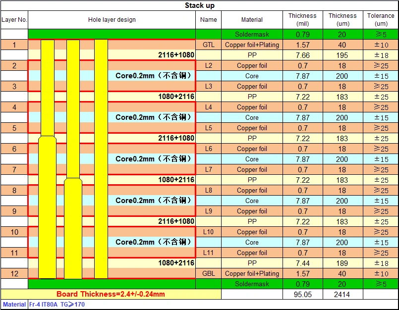
Back-drilling (controlled-depth drilling) is a critical feature of automotive backplane PCBs. By removing the unused portion of through-hole vias, back-drilling eliminates via stubs that cause signal reflections at high frequencies. This is essential for maintaining signal integrity on multi-gigabit data paths like automotive Ethernet and SerDes links.
Not every automotive interconnect is a 12-layer backplane. When the high-speed link lives on a single board — a control module, a sensor ECU, or a cockpit head unit — our 6-layer automotive PCB prototype applies the same controlled-impedance discipline at a lower layer count.
Technical Capability & Specifications
| Parameter | Specification | Advanced Capabilities |
|---|---|---|
| Layer Count | 12 Layer | 2-32L (Mass); 2-64L (Sample) |
| Base Material | FR-4 S1000-2M Tg 180 | SY, NY, TUC, ZY, EMC, KB, ITEQ, Rogers, Megtron, Nelco, Isola |
| Board Thickness | 2.4mm | 0.2-6.4mm (Mass); 0.15-20mm (Sample) |
| Panel Size | 410x150mm/1 | 800x600mm (Mass); 1050×610 (Sample) |
| Copper Thickness | Outer: 1 oz Inner: 0.5 oz | Outer: 1/3–12 oz Inner: 1/4–12 oz |
| Min Drill Size | 0.25mm | 0.127mm (Sample) |
| Min Trace Width/Spacing | 4/4 mil | 2.5/2.5 mil (Sample) |
| Back-Drill Depth | Controlled +/-0.05mm | Minimum stub: 0.10mm |
| Surface Finish | ENIG | HASL, OSP, Immersion Silver, ENIG, ENEPIG |
| Solder Mask | Green | Green, Black, Blue, Red, Yellow, White, Purple |
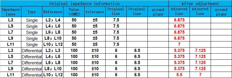
| Impedance Control | 50/85/90/100 Ohm +/-8% | +/-5% available for multi-gigabit links |
| Max Board Size | 600x500mm | 1050x610mm (Sample) |
Key Advantages of Our Automotive Backplane PCB
- Back-Drilled Via Technology: Controlled-depth back-drilling removes via stubs on signal through-holes, reducing reflections and enabling clean multi-gigabit signal transmission critical for automotive Ethernet and SerDes links.
- Symmetric 12-Layer Construction: Balanced layer stackup with equal top/bottom copper distribution prevents warpage in large-format backplane boards, critical for reliable connector mating in automotive environments.
- Multi-Reference Plane Architecture: Six ground/power planes provide continuous reference for every signal layer, ensuring consistent impedance and minimal crosstalk across long signal traces.
- IATF 16949 Automotive Quality: Full automotive quality management system with PPAP documentation, traceability, and process control for safety-critical automotive applications.
- Low-Loss Dielectric Option: Available low-loss FR-4 alternatives (Megtron 6, Nelco N4000-13) for 10+ Gbps SerDes links requiring minimal insertion loss over long trace lengths.
Overcoming Critical Challenges in Automotive Backplane Design
When sourcing high-speed backplane PCBs for automotive applications, engineers encounter three critical challenges. Here is how our engineering team eliminates them:
1. Signal Reflection from Via Stubs at Multi-Gigabit Frequencies
The Problem: Automotive backplanes route multi-gigabit SerDes and Ethernet signals through connector via fields. Unused via stubs on these signal paths cause impedance discontinuities and signal reflections, leading to bit errors and link failures at Gbps data rates.
Our Solution: Our back-drilling process uses controlled-depth drilling (accuracy +/-0.05mm) to precisely remove via stubs on signal through-holes. The remaining stub length is minimized to 0.10mm or less, effectively eliminating stub-induced reflections. This enables clean 10+ Gbps signal transmission through connector pin fields.
2. Warpage in Large-Format Backplane Boards
The Problem: Automotive domain controller backplanes are large-format boards (200mm+) with heavy connector loads. Asymmetric copper distribution causes PCB warpage, resulting in connector misalignment, BGA solder opens, and assembly failures.
Our Solution: Our 12-layer stackup is symmetrically balanced — equal copper distribution on top and bottom halves of the board. Inner signal and plane layers are arranged in mirror pairs to equalize thermal expansion. Combined with controlled lamination pressure, we achieve warpage <0.75% on backplane boards up to 600mm.
3. Signal Integrity on Long Trace Routes
The Problem: Automotive backplanes route signals across long distances (100mm+) between connectors and compute ICs. At multi-gigabit frequencies, trace loss, dielectric loss, and crosstalk degrade signal quality beyond usable limits.
Our Solution: We use tightly coupled microstrip and stripline routing with continuous ground references. Low-loss dielectric options (Megtron 6, Nelco) reduce dielectric loss. Back-drilled vias eliminate reflection points. Differential pair routing maintains tight skew (<5ps) for high-speed SerDes channels, ensuring reliable multi-gigabit data transmission.
Where Our Automotive Backplane PCBs Are Used
Our 12-layer automotive backplane PCBs power a wide range of automotive compute applications:
- ADAS Domain Controllers: Central compute platforms aggregating camera, radar, and LiDAR data via multi-gigabit SerDes links for autonomous driving functions.
- Central Gateway Modules: Vehicle network gateways routing automotive Ethernet, CAN-FD, and LIN signals between domain controllers and ECUs.
- Infotainment Compute Platforms: High-performance infotainment processors with PCIe Gen3 links to storage, display, and audio subsystems.
- Vehicle Compute Clusters: Centralized computing modules replacing distributed ECUs with high-speed backplane interconnects.
- Automotive Ethernet Switches: Multi-port automotive Ethernet switch boards for in-vehicle network backbone infrastructure.
Our Quality Guarantee for Automotive Backplane PCBs
Automotive backplane PCBs are safety-critical components that cannot tolerate failures. We implement rigorous testing protocols on every board:
- 100% AOI Inspection: Automated Optical Inspection scans every layer for trace breaks, shorts, and alignment errors.
- 100% Electrical Testing (E-Test): Fixture-based testing with back-drilling verification on every signal via.
- Controlled Impedance Testing: Polar Instruments test report documenting 50/85/90/100 ohm compliance for every batch.
- Back-Drill Depth Verification: Cross-section verification of back-drill depth and stub length on sample boards.
- Certifications: ISO 9001:2015, ISO 14001, IATF 16949, UL (E305905), RoHS compliant. IPC Class 3 available for safety-critical automotive applications.
Why Choose Season PCB for Your Automotive Backplane PCB?
With nearly 20 years of experience in PCB manufacturing, Season Multilayer Circuit has served over 8,000 global clients in automotive electronics, telecommunications, and aerospace. Our three manufacturing facilities provide capacity for both rapid prototyping and high-volume automotive production.
We understand that automotive backplane PCBs are safety-critical components. That is why every 12-layer automotive backplane PCB we ship is backed by:
- Free DFM file checking before production — including signal integrity review
- 24/7 dedicated engineering support — including back-drilling consultation
- Guaranteed on-time delivery
- No minimum order quantity — from 1 prototype to 50,000+ units
- Engineering fee waivers on bulk production orders
Season PCB specializes in 12-layer automotive backplane PCB manufacturing for ADAS domain controllers and central gateway modules. Our automotive backplane PCB products feature back-drilled via technology, multi-reference plane architecture, and IATF 16949 certified quality. Each automotive backplane PCB meets IPC standards.
For your automotive backplane PCB needs, Season PCB provides fast turnaround, competitive pricing, and IATF-certified quality. Contact us for automotive backplane PCB manufacturing today.
Our automotive backplane PCB boards comply with UL safety certifications and IPC manufacturing standards. Each automotive backplane PCB undergoes back-drill verification and signal integrity testing. The same build scales to high volumes on 998PCB Group’s high-speed and high-frequency PCB lines at the group’s Shenzhen campus.
Backplanes that carry an RF front-end alongside high-speed SerDes can drop in our low-loss Rogers laminates for the radio section.
Frequently Asked Questions
What is back-drilling and why is it important for automotive backplanes?
Back-drilling is a controlled-depth drilling process that removes the unused portion (stub) of through-hole vias on signal layers. Via stubs cause signal reflections at multi-gigabit frequencies, leading to bit errors. By removing stubs, back-drilling enables clean signal transmission for automotive Ethernet (1-10 Gbps) and SerDes links used in ADAS and infotainment systems.
What materials do you recommend for multi-gigabit automotive backplanes?
For signals up to 5 Gbps, standard FR-4 S1000-2M (Tg 180) provides adequate performance. For 5-10 Gbps, we recommend low-loss materials like Megtron 4 or N4000-13. For 10+ Gbps, Megtron 6 or Rogers RO4350B provides the lowest dielectric loss. Material selection depends on trace length and signal rate.
Can you provide PPAP documentation for automotive qualification?
Yes, as an IATF 16949 certified manufacturer, we provide full PPAP (Production Part Approval Process) documentation including control plans, FMEA, MSA, and capability studies. This documentation supports automotive OEM and Tier-1 supplier qualification requirements.
What materials and surface finishes are available for the 12-layer automotive backplane PCB?
The standard build is FR-4 S1000-2M (Tg 180) at 2.4mm board thickness, with SY, NY, TUC, ZY, EMC, KB, ITEQ, Rogers, Megtron, Nelco, and Isola laminates available on request; low-loss options such as Megtron 6 and N4000-13 support 10+ Gbps SerDes links. Copper is 1 oz outer and 0.5 oz inner, expandable up to 12 oz. ENIG is the standard surface finish, with HASL, OSP, immersion silver, and ENEPIG optional. Solder mask is green as standard, with black, blue, red, yellow, white, and purple available.
How do you verify quality on automotive backplane PCBs?
Every board passes 100% AOI scanning every layer for trace breaks, shorts, and alignment errors, plus 100% fixture-based electrical testing with back-drilling verification on every signal via. Each batch ships with a Polar Instruments impedance test report documenting 50/85/90/100 ohm compliance, and back-drill depth and stub length are verified by cross-section on sample boards. We operate an IATF 16949 certified quality management system with PPAP documentation and full traceability, alongside ISO 9001:2015, ISO 14001, UL (E305905), and RoHS; IPC Class 3 is available for safety-critical applications.
Ready to start your Automotive Backplane PCB project?
Whether you need 5 pieces for prototyping or 50,000 for mass production, our engineering team is ready to support your automotive backplane project with DFM review, signal integrity analysis, and fast-turn fabrication.
Tel: (+86) 18681528532 (WhatsApp)
E-mail: roc@season-pcb.com