Book Appointment Now

Where an HDI PCB lead time actually goes: repeated press cycles, laser capacity, yield holds and material availability, with typical ranges by stage count.
Why HDI PCB Lead Time Runs Longer Than a Standard Board
HDI PCB lead time is quoted as a single number, but it is produced by a chain of decisions that mostly have nothing to do with layer count. Two boards with the same stack thickness and the same copper weight can differ by a week or more purely because one of them re-enters the lamination, drilling and plating loop three times and the other enters it once. Buyers who understand that chain can plan around it; buyers who treat it as a fixed attribute end up compressing the wrong end of their project.
This article separates the four things that actually consume calendar days in an HDI build – repeated process cycles, laser drilling capacity, yield holds and material availability – then gives typical ranges by stage count and the design and purchasing moves that reliably pull days out of the schedule without cutting corners on inspection.
Table of Contents
- Why HDI PCB Lead Time Differs From a Through-Hole Build
- What a Standard Board Spends Its Days On
- Press Cycles Repeat the Same Work, and the Queue With It
- Laser Drilling Is a Narrower Pipe Than Mechanical Drilling
- Where the Days Accumulate, Block by Block
- Typical HDI PCB Lead Time Ranges by Configuration
- Yield and Rework Are Scheduled Risk, Not Bad Luck
- Material and Panel Availability Set the Floor
- How to Shorten HDI PCB Lead Time Without Cutting Inspection
- Planning Your Milestones Around the Real Lead Time
- FAQ
- Get a Date That Reflects Your Actual Route
Why HDI PCB Lead Time Differs From a Through-Hole Build
A through-hole multilayer board passes through the fabrication line once: image the inner layers, press the stack, drill, plate, mask, finish, test, ship. An HDI board passes through the press, drill and plate portion of that line once for every build-up layer pair. The layers do not simply stack up in thickness; the panel physically re-enters the same equipment, re-queues behind other work and re-passes the same inspection gates.
That repetition is why HDI and standard boards diverge on schedule well before they diverge on material cost. A ten-layer through-hole board and an eight-layer two-stage HDI board may need a similar amount of laminate, but the HDI board needs three press cycles instead of one, two laser passes per side instead of none, and a via fill step between each cycle.
The practical consequence is that schedule questions on an HDI programme should be asked in stage counts, not layer counts. “How long for eight layers” has no single answer; “how long for eight layers at two stages” does.
What a Standard Board Spends Its Days On
Every PCB order carries a fixed set of blocks regardless of technology. Engineering and CAM consume the first block: the data package is checked for annular ring, soldermask clearance, panelisation and drill fit, and any query has to come back to you before tooling is released. Inner-layer imaging and etching follow, then lamination, then mechanical drilling and plating, then solder mask and surface finish, then electrical test and final inspection.
On a through-hole board each of these blocks happens once, and most of them run in parallel across the panel population of the order. The queue time inside a block is usually longer than the process time, which is why shop loading matters as much as the technical route: a board that arrives when the press is fully booked waits, no matter how simple it is.
This is the baseline an HDI quote extends. Everything below adds to it rather than replacing it, which is why an HDI schedule is never shorter than the through-hole route for the same layer count.
Press Cycles Repeat the Same Work, and the Queue With It
A one-stage HDI build needs two press cycles, a two-stage build three, and a three-stage build four or more. Between any two cycles the panel must be drilled, plated and prepared again, so the repeated unit is not just the press operation – it is image, press, drill, plate, and the handling and inspection around them.
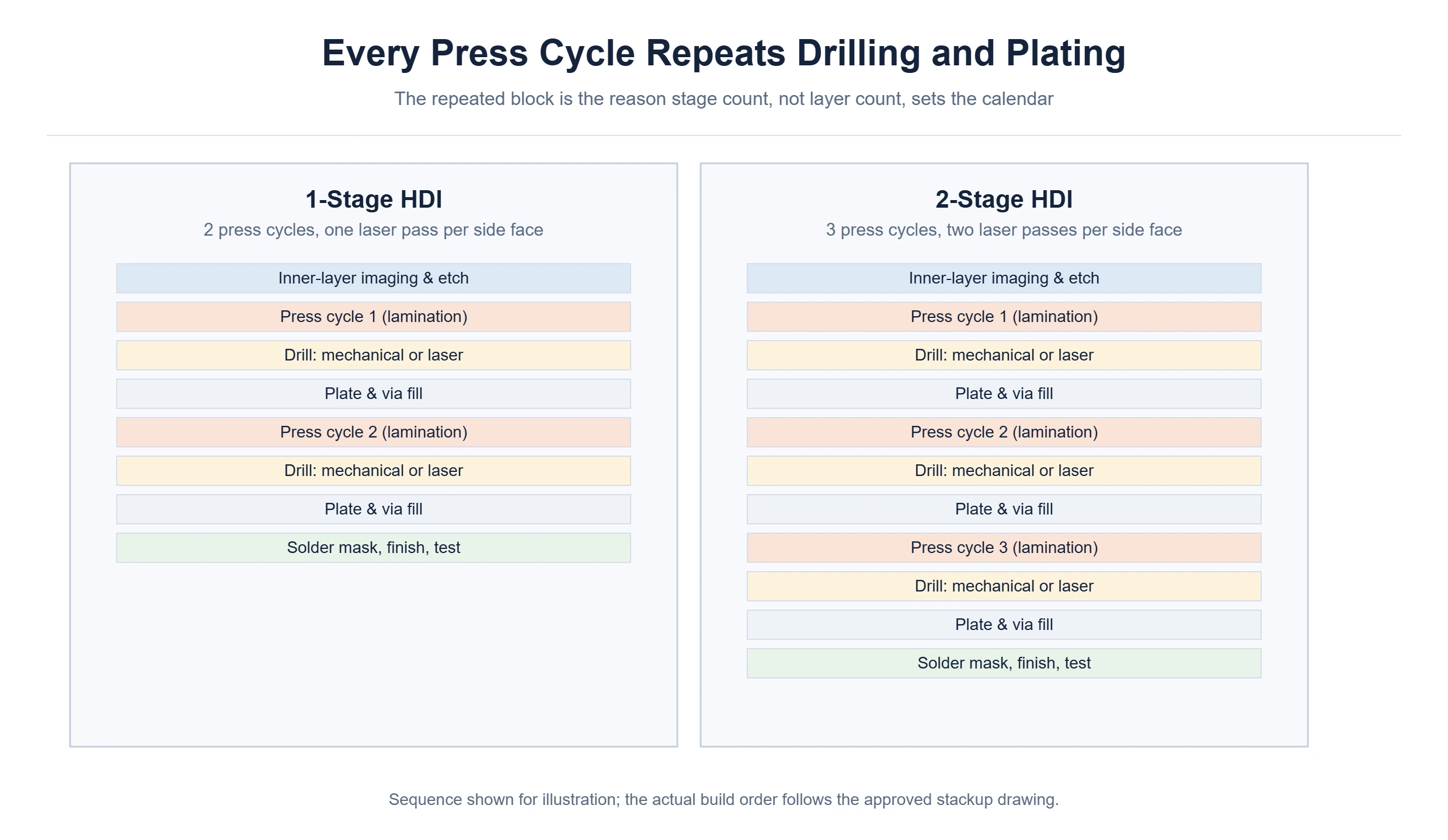
Each re-entry also re-queues. A through-hole panel competes for the drill once; a two-stage panel competes for the press three times and for laser drilling twice per side. When the shop is heavily loaded, the waiting time added by those extra queue positions is often larger than the process time itself, which is why lamination scheduling is the first thing to ask about when a delivery date looks tight.
It is also why stage reduction is the single most effective schedule lever available to a designer. Removing one stage removes one press cycle, one laser pass per side and one full trip through drilling and plating – days of process time and, at busy times, days of queue time as well.
Laser Drilling Is a Narrower Pipe Than Mechanical Drilling
Mechanical drilling capacity is broad: many spindles, many machines, and a mature queue discipline. Laser drilling for microvias is a much narrower resource. The hole is typically 0.1 to 0.15 mm, the equipment is specialised, and each layer pair with its own via size needs its own program and its own registration setup. A board with three microvia diameters across two stage pairs is not three times the work of one diameter – it is more, because setup is per combination.
The difference between mechanical and laser drilling therefore shows up twice in the schedule: once as process time, and once as sensitivity to how many other HDI jobs are in the laser queue that week. Two fabricators with identical equipment can quote different dates because one has a hole in its laser loading and the other does not.
Practical advice that follows: keep the number of distinct microvia diameters in a design to a minimum, and avoid introducing a new via size late in the programme. Each new size is new programming and a new plating recipe, and both are set-up time that lands directly on the calendar.
Where the Days Accumulate, Block by Block
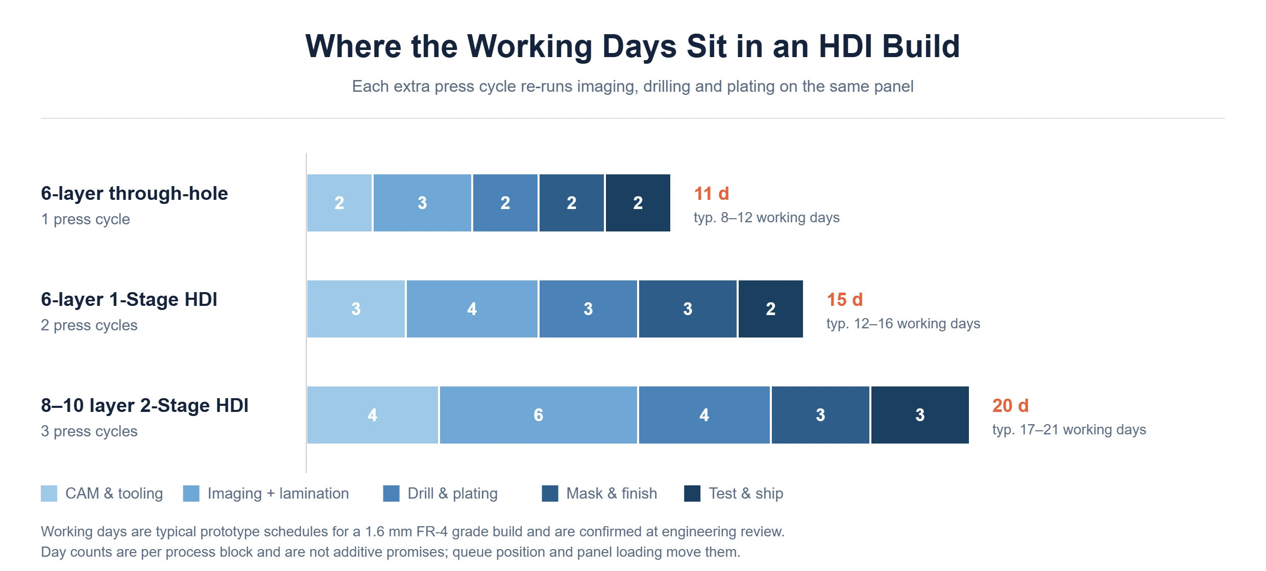
Breaking the schedule into the same five blocks for each build makes the accumulation visible. The numbers below are typical working days for a 1.6 mm FR-4 grade prototype, not commitments; queue position at the time of order moves them by more than most design changes do.
| Process block | 6-layer through-hole | 6-layer 1-Stage HDI | 8–10 layer 2-Stage HDI | 10-layer 3-Stage HDI |
|---|---|---|---|---|
| Engineering, CAM and tooling | 2 days | 3 days | 4 days | 4–5 days |
| Imaging and lamination | 3 days, 1 press | 4 days, 2 presses | 6 days, 3 presses | 8 days, 4 presses |
| Drilling and plating | 2 days, mechanical | 3 days, 1 laser pass per side | 4 days, 2 laser passes per side | 5 days, 3 laser passes per side |
| Solder mask and surface finish | 2 days | 3 days | 3 days | 4 days |
| Electrical test and final inspection | 2 days | 2 days | 3 days | 3 days |
| Typical prototype total | about 8–12 working days | about 12–16 working days | about 17–21 working days | about 20–26 working days |
Read the table as a shape rather than as a promise. The blocks that grow fastest are the ones that repeat – lamination, and drilling and plating. Engineering also grows, but for a different reason: more layer pairs mean more film sets, more drill programs and more stackup verification before the first panel is released.
Typical HDI PCB Lead Time Ranges by Configuration
Production orders run on a different curve from prototypes because the engineering work is already amortised and the process is qualified. The ranges below are for a qualified, repeat build; a first production batch after a prototype still carries part of the prototype curve while the process is being proven at volume.
| Configuration | Press cycles | Typical prototype lead time | Typical production lead time |
|---|---|---|---|
| 6-layer through-hole | 1 | 8–12 working days | 10–15 working days |
| 6-layer 1-Stage HDI | 2 | 12–16 working days | 14–20 working days |
| 8–10 layer 2-Stage HDI | 3 | 17–21 working days | 18–25 working days |
| 10-layer 3-Stage HDI | 4+ | 20–26 working days | 22–30 working days |
Three things move a board off these ranges, and only one of them is technical. The technical ones are a non-stocked laminate or a via fill specification that needs a process trial. The commercial one is loading: the same board placed in a quiet week and in a fully booked week can differ by a week or more, and no amount of design optimisation removes that. Dates are therefore confirmed at engineering review against the actual build slot, not inferred from a table.
If you need the shape of a production ramp rather than a single date, our lead time overview sets out how prototype, pilot and volume builds sit against each other, and the manufacturing capability page lists the layer counts and processes that run as standard rather than as specials.
Yield and Rework Are Scheduled Risk, Not Bad Luck
Registration tolerance accumulates with each press cycle, so a two-stage board runs a higher risk of scrap than a one-stage board of the same layer count. Fabricators plan for that: extra panels are started, and hold points are inserted where a defect is cheaper to catch. Both of those consume calendar days before anything has gone wrong.
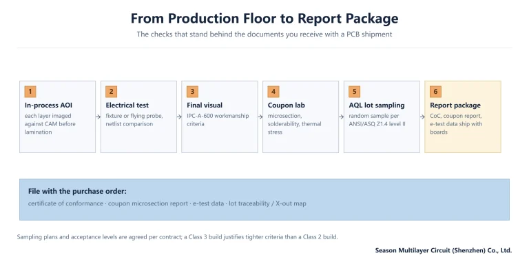
The visible part of this is the hold point after lamination and after via fill, where X-ray registration checks and coupon microsections decide whether the lot continues, judged against the acceptance criteria in IPC-6012 and IPC-6013. On a two-stage build those checks happen more than once, and each one can stop the lot for a shift while results are read. A rework, when it happens, sends the panel back into the queue rather than to the front of it – which is why one rework event can cost more days than the whole inspection programme.
Understanding this changes what a buyer should ask. The useful question is not “can you make it faster” but “which hold points are in this route, and what do you need from me before each one” – usually nothing, but occasionally a specification decision on via fill or acceptance criteria that would otherwise wait for an answer.
Material and Panel Availability Set the Floor
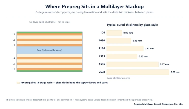
No process optimisation beats a missing laminate. Standard FR-4 grade material in common thicknesses is stocked, and prepreg in the usual glass styles is available from stock or within days. Move to a low-loss laminate, a specific Tg grade or an unusual construction and the clock starts from the material, not from the press.
The same applies to panel utilisation. A design that panels poorly wastes material and, at the margin, can force a second lamination batch where one would have done. When a programme is schedule-critical, the panelisation review is worth doing before the first build rather than after the first quote, and it belongs in the same conversation as the stackup. Our HDI technology overview covers the stackup conventions that keep builds inside standard material and standard tooling.
If your design needs a laminate that is not a stock item, say so at RFQ stage. It rarely changes the answer to “can you build it”, but it always changes the answer to “when”.
How to Shorten HDI PCB Lead Time Without Cutting Inspection
Most of the days a buyer wants back are recoverable before the order is placed, because most of the delay is queue and rework rather than process time. These levers are listed in the order their effect usually shows up.
| Lever | Typical effect on schedule | Caveat |
|---|---|---|
| Remove one HDI stage where the fanout allows | Removes one press cycle and one laser pass per side | Only valid if the escapes still close at the BGA pitch |
| Freeze the stackup before tooling release | Avoids a restart at CAM and a second film set | Requires design sign-off before the RFQ |
| Complete DFM review before release | Removes the query round trip inside the engineering block | Adds a day up front, saves more than it costs |
| Limit distinct microvia diameters | Cuts laser programming and plating setup | Constraints routing flexibility slightly |
| Pre-approve material equivalents | Avoids waiting for a substitution decision mid-build | Must be agreed in writing, not verbally |
| Share the forecast, not just the PO | Improves slot allocation on press and laser | Non-binding forecast is enough for planning |
The DFM analysis lever is consistently underrated. A query that comes back on day two of the engineering block costs a day; the same query discovered on the Gerber drill data after lamination costs a press cycle. Reviewing annular ring, mask clearance and via fill specification before release is the cheapest schedule insurance in the programme.
What does not work is compressing the inspection programme. Cutting the X-ray or coupon checks on a two-stage build does not shorten the route; it moves the discovery of a registration problem to your incoming inspection, where you have less information and no chance to recover the panel. A schedule protected that way is a schedule with the risk deferred, not removed.
Planning Your Milestones Around the Real Lead Time
Plan backwards from the assembly date and put the fabrication blocks in as blocks, not as a single number. A two-stage HDI prototype at four weeks includes a hold point after lamination where nothing can be compressed, and a first-article review where your own team has to be available. Both are calendar items on your side as much as on the fabricator’s.
Two structural moves help more than any negotiation. First, run the assembly tooling and stencil procurement in parallel with fabrication rather than after it – they do not depend on finished boards, only on the approved design. Second, decide the acceptance class and the test coverage at order placement, because those decisions sit in the engineering block and a late answer restarts it.
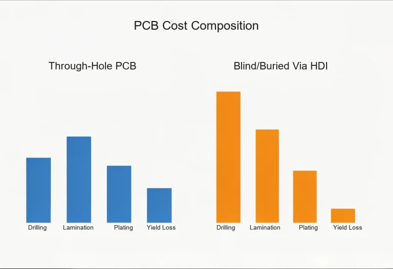
For boards where density is the open question, the cost and schedule consequences run together: every additional stage adds a press cycle as well as a premium. The breakdown of blind and buried via cost shows the same ladder from the pricing side, and the stage-count comparison shows what each rung requires in process terms. A build that holds two stages instead of three gains roughly a press cycle in schedule and a step on the premium at the same time.
Where a stackup is already fixed at three stages or more, the three-stage stackup reference sets out what the route actually contains, which is the honest basis for any date you commit to your own customer.
Frequently Asked Questions
How long does an HDI PCB take to manufacture?
A six-layer one-stage HDI prototype typically takes about 12–16 working days and an eight to ten layer two-stage prototype about 17–21 working days, with three-stage builds running 20–26 working days. Production orders on a qualified build usually add a few days rather than falling below the prototype range, because volume brings its own scheduling constraints. Dates are confirmed at engineering review against the actual build slot.
Why does an HDI board take longer than a through-hole board of the same layer count?
Because the panel re-enters the press, drill and plate loop once per build-up layer pair. A through-hole board is laminated, drilled and plated once. A two-stage HDI board goes through three press cycles and two laser passes per side, with via fill between them, so both process time and queue time multiply while the material content barely changes.
Does adding layers or adding HDI stages slow a build more?
Adding stages slows it more per unit of change. Two extra layers add imaging, lamination material and drill time in a single pass. One extra HDI stage adds a press cycle, a laser pass per side, another drilling and plating trip and another set of hold points, and each of those re-queues behind other work. That is why schedule discussions belong in stage counts rather than layer counts.
Can an HDI prototype be built faster if the design is frozen early?
Yes, and freezing early mainly protects the front of the route. A stable stackup and a complete data package remove the query round trip inside the engineering block and avoid a restart at CAM, which is where a late change costs a film set and often a press slot. It will not compress the lamination or laser blocks, but it stops days being lost before they start.
Why do two fabricators quote different lead times for the same board?
Usually because of loading rather than capability. Laser drilling and press time are narrow resources, so the date depends on what else is booked when your panel arrives. Equipment, stackup conventions and material stock also differ. Ask for the route and the hold points behind the date, not just the date, and compare those before assuming one quote is more credible.
Does the quoted lead time include first article and inspection?
It should. A realistic HDI date includes the engineering block, the press cycles, the laser work, the hold points where registration and microsection results are reviewed, electrical test and final inspection. If a date appears to exclude first-article review or coupon work, ask explicitly – those steps cannot be skipped on a two-stage build without moving the risk into your incoming inspection.
What can delay an HDI build after the order has been placed?
The common causes are a late specification decision, a stackup change after tooling release, a non-stocked laminate, and rework that sends the panel back into the queue rather than to its front. Registration-related scrap on higher stage counts is planned for by starting extra panels, but it still consumes slots. Answering via fill, acceptance class and material substitution questions at order placement removes most of the avoidable delay.
Get a Date That Reflects Your Actual Route
We build from 2 to 30 layers with one- to four-stage HDI, laser microvias down to 0.1 mm and 2/2 mil lines as standard production capability, and we quote the route behind the date rather than only the date itself. Send your Gerber data, stackup drawing and target milestone and ask which hold points your build will pass through – that list is what makes a delivery commitment defensible. Prototype builds can also be placed through the two-stage HDI prototype route if the stackup is already fixed.