Book Appointment Now

A practical guide to PCB prepreg: how glass style, resin content and resin flow set dielectric thickness, impedance and lamination quality in multilayer builds.
PCB Prepreg Explained: Glass Styles, Resin Content and Stackup Selection
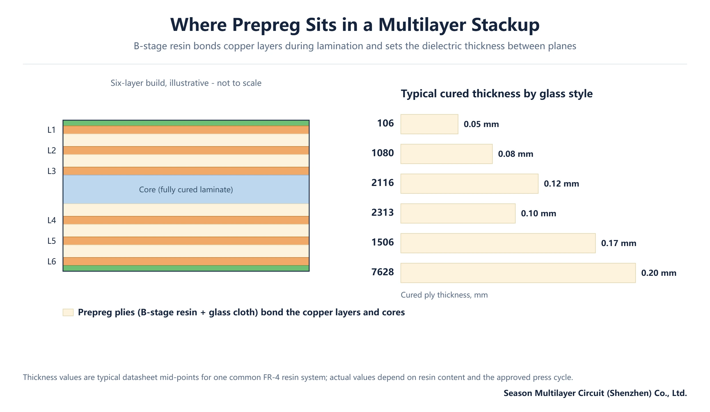
If your multilayer quote lists plies named 1080, 2116 or 7628 inside the stackup table, those lines are the PCB prepreg recipe – and they deserve more attention than they usually get. Prepreg is the semi-cured resin sheet that bonds copper layers and cores into a single board during lamination, and its glass style and resin content quietly decide your finished thickness, your dielectric spacing and, with them, your impedance. When a prototype comes back thicker than expected or a differential pair misses its impedance window, the bonding plies between the cores are very often where the story starts.
This guide explains how engineers specify PCB prepreg, what the common glass styles from 106 to 7628 actually deliver, how Dk and Df shift with resin content, and which lamination defects trace back to the bonding plies. Use it as a checklist when you review a fabricator’s stackup proposal, alongside our guides on PCB stackup design and laminate selection.
Table of Contents
- What PCB Prepreg Does in a Multilayer Stack
- How Prepreg Is Specified: Glass Style, Resin Content and Flow
- Common Prepreg Glass Styles Compared: 106 to 7628
- Prepreg Dielectric Properties: Dk and Df by Glass Style
- How PCB Prepreg Choice Sets Dielectric Thickness and Impedance
- Resin Flow, Fill and Common Lamination Defects
- Selecting Prepreg for Your Build: A Practical Checklist
- What to Confirm With Your Fabricator Before Release
- Thin Cores and HDI: Where 106 and 1080 Carry the Build
- FAQ
- Have Your Prepreg Recipe Reviewed Before Release
What PCB Prepreg Does in a Multilayer Stack
Prepreg – sometimes called B-stage resin or bonding ply – is a sheet of glass-fibre cloth pre-impregnated with partially cured epoxy resin. In its delivered state it is tacky and slightly flexible, so operators can cut it, align it and stack it between copper layers without it shifting. When the stack goes into the lamination press, heat drives the resin to full cure and pressure squeezes it into every gap around traces, planes and via holes. The result is one solid board instead of a pile of separate etched layers.
It helps to keep the two dielectric roles distinct. A core is a fully cured copper-clad laminate: rigid, dimensionally stable, and the structural backbone of the build. Prepreg is the adhesive that sits where cores meet, and it does two jobs at once – it bonds the layers together and it sets the dielectric thickness between copper planes. That second job is why your fabricator’s stackup design always lists the prepreg style and ply count per gap rather than a vague thickness promise.
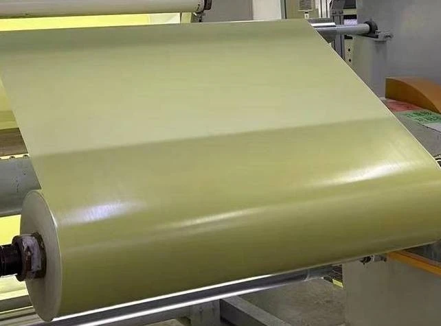
Because the resin is only partially cured, prepreg is also the most moisture- and time-sensitive material on the production floor. Fabricators store it sealed and temperature-controlled, and track its remaining shelf life. That handling discipline matters more than most buyers realise: a bonding ply that has absorbed moisture or exceeded its working life is a common root cause of voids and delamination that only show up weeks later, at assembly or in the field.
How Prepreg Is Specified: Glass Style, Resin Content and Flow
A prepreg line in a stackup table compresses three parameters into one name. The first is the glass style – the weave of the glass cloth, identified by industry numbers such as 106, 1080, 2116 or 7628. Thinner weaves carry more resin and cure to thinner plies; heavier weaves carry less resin and build thicker, stiffer dielectrics. These style numbers and the resin systems around them are catalogued in IPC-4101, the specification base for laminate and prepreg materials maintained by the IPC.
The second parameter is resin content (RC), expressed as a percentage of the ply’s weight. A 106 ply at 76% resin content is mostly resin; a 7628 ply at 44% is mostly glass. RC controls how much resin is available to flow, fill and set the final gap. The third is resin flow – how far the melted resin travels before it gels, usually graded and tuned to the press cycle. High-flow plies fill complex gaps quickly; low-flow plies hold their thickness where a controlled dielectric matters.
One more specification rides along with the resin system: flammability recognition. A bonding ply is part of the laminate system, and recognised systems carry a UL yellow-card listing for flammability class – typically UL 94 V-0 – so the finished board keeps its recognition. If your product carries a safety certification, confirm that the prepreg grade named in the stackup belongs to the recognised system, not just the core. Our overview of PCB materials and laminates covers how cores, prepregs and copper foils fit together as one qualified system.
Common Prepreg Glass Styles Compared: 106 to 7628
Six glass styles cover the overwhelming majority of multilayer work. The numbering is not a thickness rating, but there is a strong correlation: lower numbers use finer weaves and thinner plies with more resin, higher numbers use coarse weaves and thicker plies with less resin. The table below condenses the ranges a buyer will typically see quoted for a common FR-4 resin system.
| Glass style | Resin content (%) | Cured thickness (mm) | Typical role in a build |
|---|---|---|---|
| 106 | 73–78 | 0.05 | Thin dielectric plies for HDI build-up and tightly controlled stacks |
| 1080 | 65–70 | 0.07–0.09 | General-purpose thin to mid bonding plies |
| 2116 | 52–58 | 0.11–0.13 | Standard multilayer bonding between cores |
| 2313 | ≈57 | 0.10 | High-flow ply for special fills, used less often |
| 1506 | 48–52 | 0.16–0.18 | Thicker low-flow fill where spacing must hold |
| 7628 | 43–52 | 0.18–0.23 | Heavy mechanical strength; power and backplane-style builds |
In practice, 1080 and 2116 do most of the work on conventional multilayer boards, and a stackup will often mix styles in one gap – for example, one 2116 ply plus one 1080 ply to land a specific dielectric height. 106 dominates where layers sit close together, which is exactly the situation in 8-layer security and industrial builds with fine-pitch BGAs on tightly spaced planes. 7628 appears less often, mainly where a board needs mechanical robustness or a large power-plane spacing; its coarse weave also limits how well it suits fine-featured, high-frequency layers.
Prepreg Dielectric Properties: Dk and Df by Glass Style
Resin and glass have different electrical properties, so the resin-to-glass ratio moves the effective Dk and Df of the bonding ply. More resin – as in 106 and 1080 – pulls Dk down and pushes Df up; more glass – as in 7628 – pulls Dk up and Df down slightly. The table below condenses datasheet values for one representative FR-4 resin system so you can see the trend across styles.
| Glass style (RC) | Dk @ 1 GHz | Dk @ 10 GHz | Df @ 10 GHz |
|---|---|---|---|
| 7628 (43%) | 4.81 | 4.73 | 0.016 |
| 1506 (48%) | 4.70 | 4.61 | 0.016 |
| 2116 (52%) | 4.45 | 4.50 | 0.017 |
| 1080 (65%) | 4.29 | 4.18 | 0.020 |
| 106 (73%) | 4.09 | 3.97 | 0.020 |
Two cautions apply when you reuse numbers like these. First, they are typical published values for one resin system – your fabricator’s grade, and even the specific RC lot, will shift them by a few percent, so always confirm against the datasheet for the exact grade named in your stackup. Second, both Dk and Df drift with frequency: a value quoted at 1 GHz underestimates loss on a multi-gigabit link. For signal-integrity work, simulate with values at or near your actual edge rate and treat the table as a starting point, not a guarantee.
How PCB Prepreg Choice Sets Dielectric Thickness and Impedance
The distance between a signal layer and its reference plane is not set by the core alone. In a typical six- or eight-layer build, controlled pairs live over prepreg-filled gaps, so the compacted thickness of those plies after pressing is the dielectric height in your impedance model. Because impedance responds strongly to that height – roughly a 3–4% impedance shift per 10% change in spacing on a microstrip – a ply recipe that drifts by one glass style can move every trace on the layer out of band.
This is why a serious fabricator models the press outcome, not the ply thickness on the datasheet. Resin flows into the relief around traces and vias during pressing, so the compacted thickness is always thinner than the sum of loose plies; the calc depends on copper coverage on the adjacent layers. The right habit is to fix the target dielectric per gap from your impedance model, ask the fabricator to choose the glass styles and ply count that hit it after compaction, and verify the result: our PCB impedance measurement guide walks through TDR checks on the test coupon, and tolerance classes of ±10%, ±8% or ±5% should be assigned per layer pair before release.
Watch for one quiet trap in stackup reviews: two recipes can promise the same dielectric thickness while delivering different impedance, because they carry different Dk. One 2116 ply and two 1080 plies can land close on height yet differ in resin fraction, and the Dk difference is enough to matter on controlled pairs. If your fabricator proposes a swap, ask for the re-simulated impedance, not just the new thickness line.
Resin Flow, Fill and Common Lamination Defects
Prepreg has a hard job: it must liquefy, flow into every gap around copper features, wet the surfaces and gel at the same moment the press reaches full pressure. A recipe that flows too little leaves unfilled pockets; one that flows too much drains resin away from thin gaps and starves them. Most lamination-quality complaints trace back to that balance, and the fix is almost always a change in glass style, resin content or press schedule rather than a change in the core material. Our PCB lamination process guide covers the press cycle itself in detail.
| Defect | Typical root cause | First-line fix |
|---|---|---|
| Resin starvation, glass bloom at the surface | RC too low for the gap, or excess pressure squeezing resin out | Move to a higher-RC style in the affected gap and re-review the press recipe |
| Measling and small voids between plies | Trapped air or volatiles, often from moist or aged prepreg | Vacuum lamination, correct bake-out, sealed storage with shelf tracking |
| Finished thickness over target | Too many plies or higher-than-modelled flow-out | Recalculate compacted thickness from the R/C ratio and run a trial press |
| Impedance outside the agreed band | Dielectric height drift from a style or ply-count substitution | TDR the first-article coupon and re-simulate before lot release |
| Delamination after moisture exposure | Water absorbed by stored prepreg before pressing | Confirm fabricator storage discipline and incoming-bake practice |
None of these defects is exotic, and all of them are cheap to prevent at the recipe stage and expensive to find at receiving inspection. When a supplier quotes an unusually thin board or an unusually tight impedance window at a low relative cost, the bonding-ply recipe is one of the first places to look for the shortcut.
Selecting Prepreg for Your Build: A Practical Checklist
You rarely choose a prepreg brand as a buyer – you choose outcomes, and the fabricator translates them into plies. Still, the review you run before release should follow the same logic a process engineer uses. Work through these steps in order:
- Fix the target dielectric thickness for every layer pair from your impedance model, not from a generic stackup template.
- Prefer glass styles that hit each target with one or two plies; four or more plies in one gap invites thickness spread and voids.
- Check Dk and Df at the frequency your signals actually run at, and confirm the resin system matches your loss budget.
- Balance resin content against fill: high-RC styles for gaps crowded with vias and fine features, lower-RC styles where spacing must hold.
- Ask for the fabricator’s compacted-thickness calculation and press recipe for the exact copper coverage of your design.
- Keep core and prepreg in the same recognised resin system, and carry that system through every layer of the stack.
If a proposed stackup cannot answer items three and five with numbers, that is a signal to slow the release down. The questions cost an hour; the re-spins they prevent cost weeks.
What to Confirm With Your Fabricator Before Release
The final step is turning the checklist into commitments. Three confirmations belong in every engineering review for a multilayer build. First, the thickness budget: a per-gap dielectric table showing glass style, ply count and compacted thickness, so the finished board has a documented target. Second, the coupon plan: where the test coupon sits on the panel and which measurements it supports, so impedance and microsection results are traceable to your lot rather than to a generic process capability. Third, material handling: how prepreg is stored, how long it may wait after opening, and what bake-out runs before pressing.

These points are exactly what a DFM review should surface before tooling starts, and our PCB DFM analysis checklist lists them in submission-ready form. A fabricator who answers them without prompting is telling you something useful about their process discipline; one who treats the bonding-ply recipe as a proprietary afterthought is telling you something too.
Thin Cores and HDI: Where 106 and 1080 Carry the Build
HDI construction pushes prepreg selection to its limits. Build-up layers sit directly over dense microvia fields, dielectric spacing shrinks below what standard styles can deliver, and every extra micron of resin thickness weakens the laser-drilling window. That is why 106 and 1080 dominate HDI stacking: fine weaves with high resin content give thin, well-filled dielectrics that a 0.1 mm laser via can punch through cleanly, layer after layer.
The same logic scales up. On a 10-layer 2-stage HDI prototype, each build-up gap is specified ply by ply, and the sequential-lamination cycle means the bonding recipe is locked twice – once for the inner sub-composite and once for the outer build-up. A late substitution in either pass changes both thickness and Dk on finished layers. For a deeper view of how these builds stack up layer by layer, see the site’s HDI PCB technology guide.
The practical takeaway carries across every technology level: prepreg is not packaging material, it is the electrical structure of your board. Treat the bonding-ply recipe with the same rigour as the laminate grade and the copper weights, and the two most common multilayer surprises – thickness drift and impedance misses – stop happening to you.
Frequently Asked Questions
What does PCB prepreg actually do in a multilayer board?
It bonds copper layers and cores into one solid board during lamination and sets the dielectric thickness between them. Because it flows around traces and vias under heat and pressure, the bonding ply also determines how well gaps fill and how consistent the finished board thickness stays across a panel.
Which prepreg glass styles are most common?
1080 and 2116 cover most conventional multilayer work: 1080 for thin to mid gaps, 2116 for standard bonding between cores. 106 dominates HDI build-up because its fine weave and high resin content support thin dielectrics for 0.1 mm laser vias, while 7628 appears mainly where mechanical strength or thick power-plane spacing matters.
How does resin content affect the finished board?
Resin content controls how much material is available to flow and fill. High-RC plies such as 106 (73–78%) suit gaps crowded with features; lower-RC plies such as 7628 (43–52%) hold spacing but fill less. RC also shifts the cured thickness and the effective Dk of the ply, so both electrical and mechanical outcomes depend on it.
Can a prepreg substitution change my impedance?
Yes. Impedance depends on dielectric height and on the effective Dk of the gap, and both change when the glass style or ply count changes. Two recipes can match on thickness yet differ in Dk enough to move controlled pairs out of band, so any substitution should come back with a re-simulated impedance and a coupon TDR result.
What is the difference between prepreg and core?
A core is a fully cured, copper-clad laminate – the rigid structural layer of the board. Prepreg is only partially cured (B-stage), so it softens and flows in the press, bonds the layers together and cures into the dielectric between cores. Cores carry copper on their surfaces; prepreg provides the bonded spacing.
How many prepreg plies can be stacked in one gap?
One or two plies is the comfortable range for controlled dielectrics; more plies raise the risk of thickness spread, trapped air and uneven fill. If a target thickness needs four or more plies, the better move is to switch to a thicker glass style or adjust the core arrangement rather than pile up thin plies.
How should prepreg be handled before lamination?
Sealed, temperature-controlled storage with shelf-life tracking, minimal exposure after opening, and a bake-out before pressing when required. A bonding ply that absorbs moisture or ages past its working life is a frequent root cause of voids, measling and delamination that surface later at assembly or in the field.
Have Your Prepreg Recipe Reviewed Before Release
Send us your Gerber data and stackup intent, and our engineering team will return a per-gap bonding-ply table with compacted thickness, Dk values at your signal frequencies, and the coupon plan that verifies both – before tooling starts. Start with a stackup review and keep your next multilayer build on its impedance window from the first press.