Skip to content
  • Home
  • Services
  • Products
    • Fast PCB
    • Multilayer PCB
    • HDI PCB
    • High Speed PCB
    • High Frequency PCB
    • Rigid-Flex PCB
    • PCBA
  • Instant PCB Quote
  • About Us
    • Company Profile
    • Factory Display
    • Process Capability
    • Lead Time
    • HDI PCB Technology
    • PCB Materials and Laminates
  • News
  • Contact

Book Appointment Now

(+86) 1868152853224/7 Emergency Phone
Season PCB logo - PCB manufacturer in Shenzhen, China
  • Home
  • Services
  • Products
    • Fast PCB
    • Multilayer PCB
    • HDI PCB
    • High Speed PCB
    • High Frequency PCB
    • Rigid-Flex PCB
    • PCBA
  • Instant PCB Quote
  • About Us
    • Company Profile
    • Factory Display
    • Process Capability
    • Lead Time
    • HDI PCB Technology
    • PCB Materials and Laminates
  • News
  • Contact
(+86) 1868152853224/7 Emergency Phone
Season PCB logo - PCB manufacturer in Shenzhen, China

PCB Basics

Bare copper circuitry exposed on a PCB after the soldermask was removed, the starting point of controlled layer-by-layer analysis

PCB Reverse Engineering for Legacy Boards: Process and Limits

Gold-finished PCB rings and contact pads showing the uniform, mirror-bright deposit typical of an ENEPIG surface finish

ENEPIG Surface Finish: Pros, Cons and When to Specify It

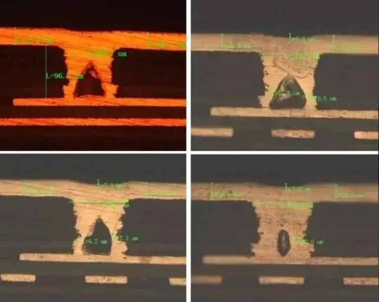
Four cross-section photos of blind vias with copper filling voids of different shapes

Plating Voids in Microvias: Root Causes and How Factories Fix Them

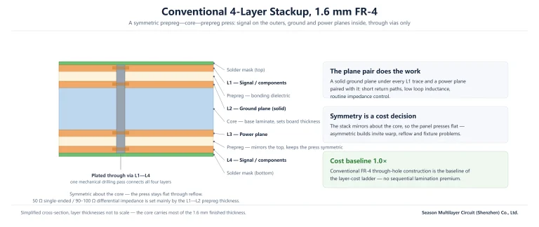
Cross section of a conventional 4-layer PCB stackup: signal layers on the outers, ground and power planes inside, symmetric prepreg-core-prepreg press with a plated through via

4-Layer PCB Cost: What Drives the Price and How to Quote It Right

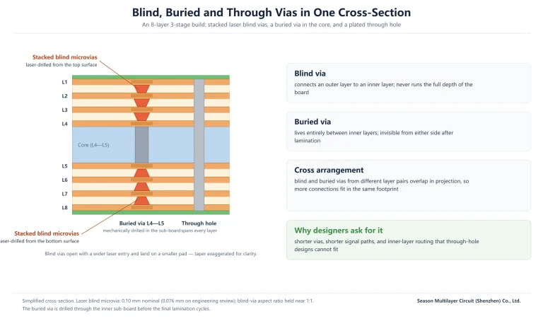
Eight-layer 3-stage HDI cross-section with stacked laser blind microvias drilled from both outer surfaces, a buried via through the core and a plated through hole

Blind and Buried Via HDI: Cross Via Structures for High-Density PCBs

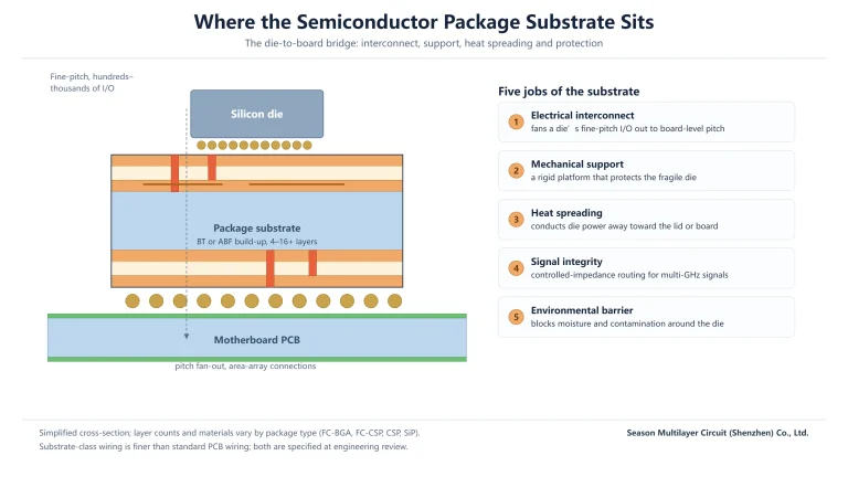
Cross-section showing a silicon die, flip-chip bumps, the package substrate and BGA balls connecting to a motherboard PCB

Semiconductor Package Substrate Explained: Functions, Materials and Types

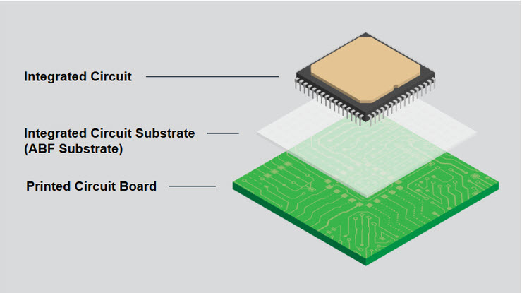
Exploded view of an IC package showing the die, ABF substrate and host PCB stack

ABF Substrate Explained: Build-Up Film, Fine Lines and FC-BGA

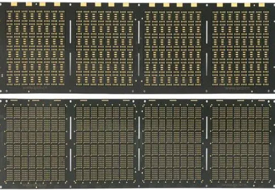
BT substrate memory package panels with gold-plated bonding pads in panel format

BT Substrate Explained: Properties, Applications and Selection

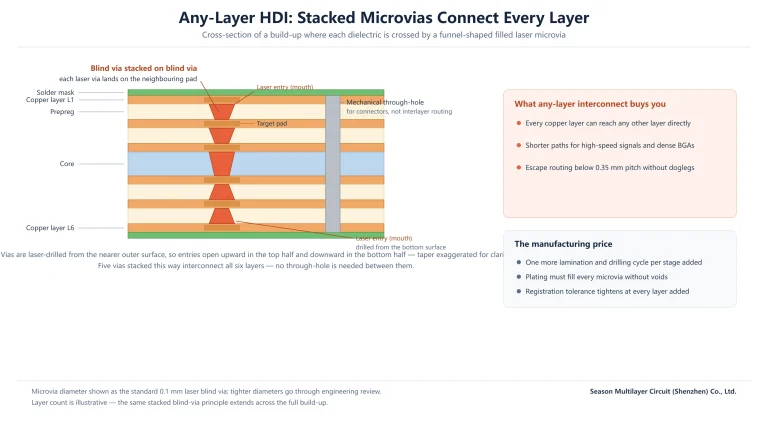
Cross section diagram of any-layer HDI with funnel-shaped laser blind vias stacked on landing pads, entries opening upward from the top surface and downward from the bottom surface, next to a mechanical through-hole

Why Advanced HDI PCB Manufacturing Is Hard: Microvias, Yield and Cost

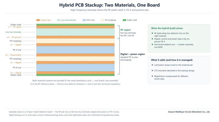
Cross section of a 6-layer hybrid PCB stackup with the RF signal and ground pair on a low-loss laminate above FR-4 cores carrying the digital and power layers

Hybrid PCB Stackup Guide: Mixed Dielectric Materials, Cost and Uses

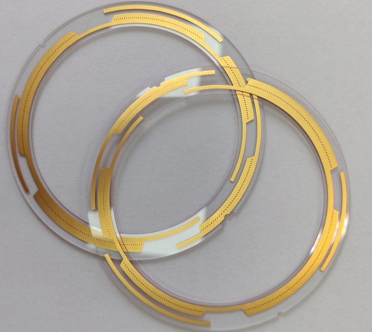
Transparent glass substrate panels with patterned gold interconnect traces, an example of glass-based circuit fabrication

Glass Substrate PCB Explained: Properties, TGV and Where It Fits

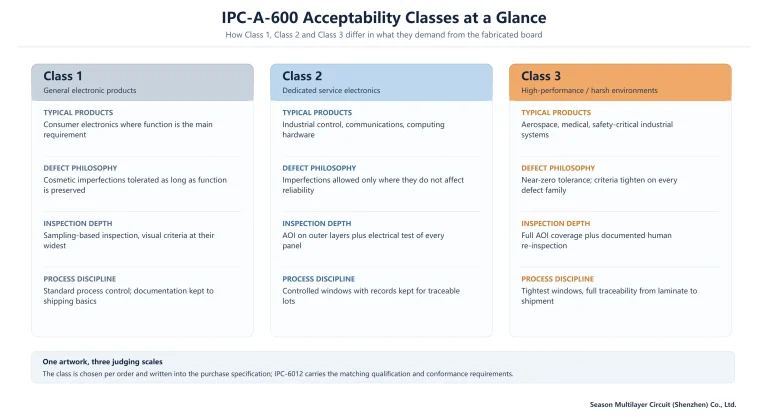
Comparison diagram of IPC-A-600 Class 1, Class 2 and Class 3 acceptance levels: typical products, defect tolerance, inspection depth and process discipline

IPC-A-600 Class 3 Explained: Requirements, Inspection and Cost Impact

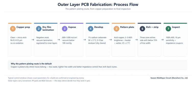
Seven step outer layer PCB fabrication flow from copper prep and dry film imaging to pattern plating, etching and AOI inspection

Outer Layer PCB Fabrication: Pattern Plating to Final Etch

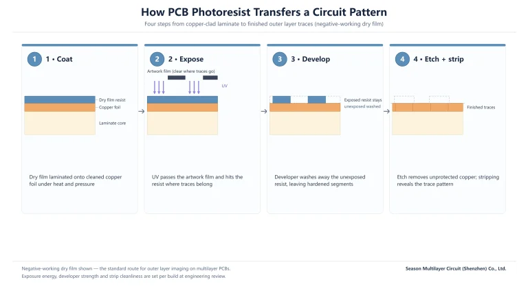
Four step diagram of PCB photoresist imaging: laminate dry film, expose through artwork, develop and etch to finished traces

PCB Photoresist Explained: How Circuit Imaging Actually Works

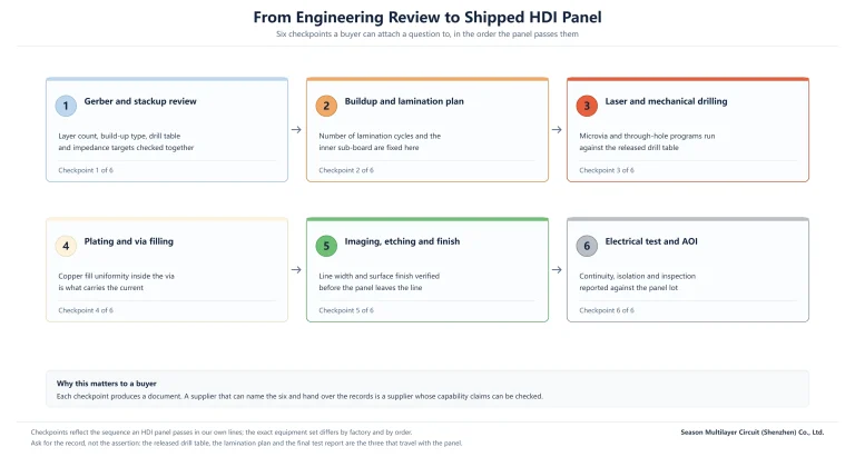
Six checkpoints from Gerber and stackup review to electrical test and AOI for an HDI panel, each producing a document a buyer can request

HDI PCB Manufacturer: How to Read a Factory’s Real Capability

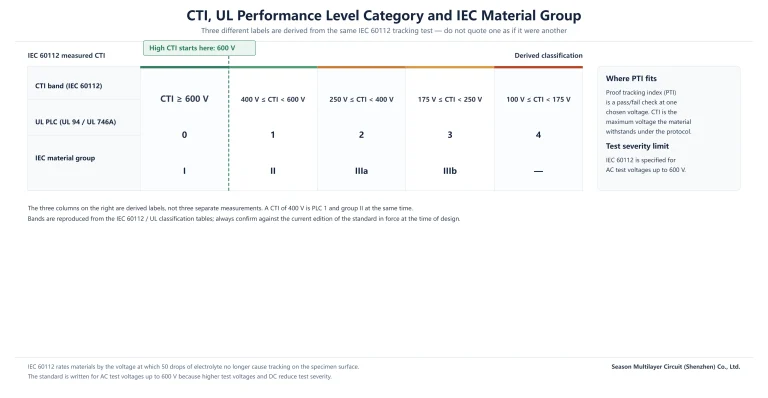
Table relating IEC 60112 CTI voltage bands to UL performance level categories and IEC material groups, with the 600 V high CTI threshold marked

High CTI PCB Explained: Ratings, Creepage Rules and Material Choice

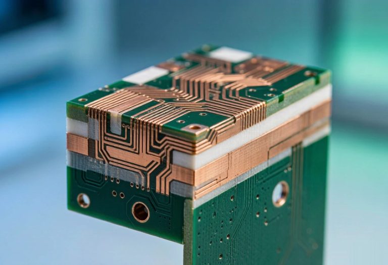
Layered PCB laminate construction showing copper foil, prepreg and core materials

PCB Laminate Selection Guide: From Standard FR4 to Low-Loss Materials

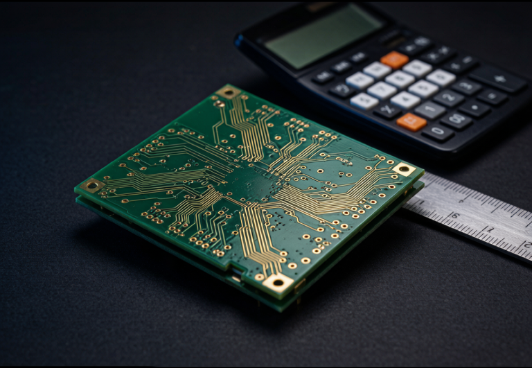
Multilayer PCB placed beside a calculator and a steel ruler, illustrating how per-area board pricing is measured

PCB Cost per Square Meter: How Quotes Are Built and Compared

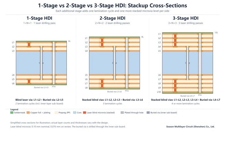
Cross-section diagrams comparing 1-stage, 2-stage and 3-stage HDI stackups, with a legend for cores, prepreg, stacked laser microvias, buried vias and plated through holes

HDI Stages Explained: 1-Stage, 2-Stage and 3-Stage PCB Stackups

Components of PCB prices shown with a multilayer circuit board, quote documents and a calculator

Components of PCB Prices: A Practical Cost Guide for Engineers and Buyers

Prev
1 2 3
Next
About Us
We are a professional manufacturer specialized in HDI and multilayer PCBs, focusing on advanced manufacturing processes for high-end HDI, multilayer PCBs, flexible printed circuits (FPCs), and rigid-flex boards, along with comprehensive services including SMT processing and PCBA OEM/ODM solutions with material procurement.
Main Products
HDI PCB
Fast PCB Sample
Multilayer PCB
High Frequency PCB
High Speed PCB
Rigid-Flex PCB
PCBA turnkey service
Know Us
Company profile
Factory Display
Process Capability
Production Time
PCB Basics
PCB industry news
Address
7F, Block A, Junfeng Business Building, 176 Chongqing Road, Fuhai Street, Baoan District, Shenzhen 518103
Tel: +86 18681528532
E-mail: roc@season-pcb.com

Copyright © 2006-2026 Season Multilayer Circuit (Shenzhen) Co., Ltd.