Book Appointment Now

What a BT substrate is, how bismaleimide triazine resin compares with FR-4 and ABF, and which package types it serves — a practical guide for hardware buyers.
BT Substrate Explained: Properties, Applications and Selection
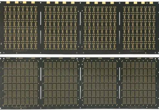
If your product uses DRAM, NAND flash, an SSD controller, or a 5G RF front-end module, the chip inside it is almost certainly mounted on a BT substrate — yet most hardware teams spend all of their review time on the host board and almost none on this layer. When a package fails in reflow or drifts out of spec in the field, the root cause is often a substrate property nobody checked: glass transition temperature, coefficient of thermal expansion, or dielectric loss.
This guide explains what a BT substrate is, how bismaleimide triazine resin differs from standard FR-4 and from ABF film, where it is used, and what its properties mean for the PCB that has to carry the finished package. The goal is practical: by the end you should know which class of substrate your chips use and what to ask your board supplier for.
Table of Contents
- What Is a BT Substrate?
- Why Chip Packaging Outgrew Standard FR-4
- BT Substrate Properties That Matter for Reliability
- How a BT Substrate Is Manufactured
- BT Substrate vs ABF vs Polyimide: Choosing the Right Class
- Where BT Substrates Are Used
- From Package Substrate to PCB: What the Board Designer Owns
- BT Substrate Selection Checklist for Buyers
- Common BT Substrate Specification Mistakes
- FAQ
- Designing the Board That Carries Your BT-Packaged Chips?
What Is a BT Substrate?
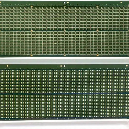
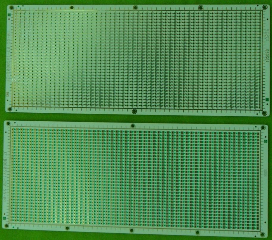
A BT substrate is an IC package substrate whose core dielectric is made from BT resin — bismaleimide triazine — reinforced with glass fabric and clad with copper. BT resin was developed in Japan in the 1980s specifically to solve a problem that conventional epoxy laminates could not: surviving lead-free assembly temperatures and repeated thermal cycling without softening, delaminating, or carbonizing.
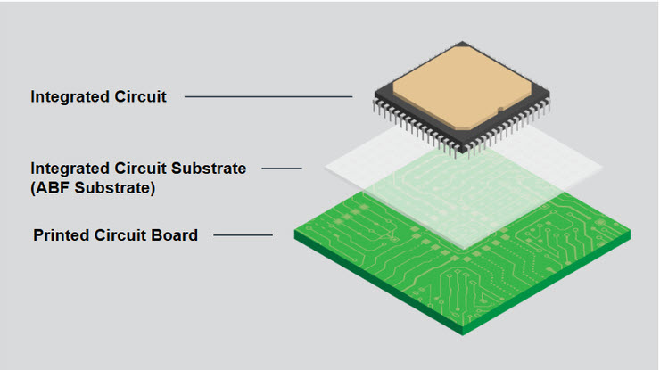
In the electronics stack, a BT substrate sits one level below the host PCB. The silicon die is attached to the substrate, the substrate’s fine-line layers redistribute the die’s bond pads to a coarse, assembly-friendly ball grid array, and the BGA balls then connect to the PCB. It is the bridge between semiconductor-scale geometry and board-scale geometry, providing electrical redistribution, mechanical support, and a heat path at the same time.
By most industry estimates, well over half of all IC packages by volume use BT-class laminates, which makes this resin system the highest-volume package substrate material in the world. That scale matters for buyers: it means mature supply chains, well-characterized reliability data, and cost positions that newer materials cannot yet match.
Why Chip Packaging Outgrew Standard FR-4
In the wire-bond era, packages were simple: a leadframe, an epoxy encapsulant, and in many cases no organic substrate at all. FR-4 — or sometimes plain phenolic board — was good enough because signal speeds were low and package geometries were coarse. Ball grid array and chip-scale packaging changed that completely. Suddenly hundreds of connections had to be redistributed under a die, in a space a few millimeters across, and the whole assembly had to survive multiple lead-free reflow passes.
Standard FR-4 struggles on three fronts. Its glass transition temperature of roughly 130–160 °C sits uncomfortably close to soldering temperatures. Its in-plane coefficient of thermal expansion of 14–18 ppm/°C is five to six times that of silicon at about 3 ppm/°C, so every thermal cycle works the solder joints like a fatigue test. And its dielectric loss is too high for the multi-gigahertz signals that modern memory and RF interfaces move across the substrate.
BT resin was formulated to close exactly those gaps, and the properties in the next section show how wide the resulting margin is. The same logic later produced other specialty dielectrics — ABF film for ultra-fine-line processor packages, and polyimide for extreme-temperature niches — but BT remains the volume workhorse in between.
BT Substrate Properties That Matter for Reliability
The thermal case is the easiest to state. A BT substrate typically has a glass transition temperature between 170 and 220 °C — a comfortable margin above lead-free reflow — and a thermal decomposition temperature above 350 °C, so the material does not degrade or carbonize even after multiple soldering cycles. In wide-temperature environments such as automotive cabins or industrial equipment, where assemblies see roughly −40 °C to +125 °C in service, that thermal headroom is what keeps the package rigid and dimensionally stable.
The mechanical case is about expansion matching. BT laminates run 10–16 ppm/°C in the X/Y plane and 30–40 ppm/°C through the Z axis, far closer to silicon than standard FR-4. Less mismatch means less stress on solder balls and wire bonds, which is precisely why BT substrates dominate BGA and CSP formats where joint failure is the dominant wear-out mechanism.
Electrically, BT resin holds dielectric constant around 3.4–4.2 and dissipation factor around 0.008–0.012, low enough to keep high-frequency losses acceptable in RF front-ends and fast memory interfaces. Volume resistivity in the region of 10¹⁴ Ω·cm, together with moisture absorption well below that of standard FR-4 (which sits near 0.8%), protects insulation resistance in humid environments. Flammability is rated UL 94 V-0 without additional flame-retardant additives, keeping end products compliant with safety requirements. The table below consolidates the typical values worth checking on any datasheet.
| Property | Typical BT substrate value | Why it matters |
|---|---|---|
| Glass transition temperature (Tg) | 170–220 °C | Stays rigid through lead-free reflow and sustained operating heat |
| Thermal decomposition temperature (Td) | ≥ 350 °C | No carbonization or degradation over repeated soldering cycles |
| CTE, X/Y plane | 10–16 ppm/°C | Close to silicon (~3 ppm/°C), reducing solder-joint fatigue |
| CTE, Z axis | 30–40 ppm/°C | Limits via stress and plated-hole strain during cycling |
| Dielectric constant (Dk) | 3.4–4.2 | Predictable impedance for high-speed routing |
| Dissipation factor (Df) | 0.008–0.012 | Low loss for RF and multi-gigabit signals |
| Water absorption | < 0.5% (some grades < 0.1%) | Insulation stability in humid operating environments |
| Flammability | UL 94 V-0 | Meets end-product safety requirements without extra additives |
One caution when comparing datasheets: these are typical published ranges for the resin class, and individual grades vary. Always confirm the specific laminate grade, resin content, and glass style in the package datasheet rather than assuming class-level numbers, and treat the values as inputs to your own reliability budget rather than guarantees.
How a BT Substrate Is Manufactured
Making a BT substrate blends conventional PCB process steps with semiconductor-grade precision. The flow below is typical; individual substrate suppliers may add or reorder steps, but every high-volume line covers the same ground.
- Prepreg and lamination. BT resin is impregnated into glass cloth to form prepreg, then copper foil and prepreg layers are stacked and pressed at roughly 180–220 °C under several MPa of pressure to cure the multilayer core.
- Precision drilling and metallization. Mechanical and laser drilling create the vias — laser drilling can reach around 50 µm diameters for high-density builds — followed by electroless and electrolytic copper plating to metallize the hole walls.
- Fine-line patterning. Dry-film or liquid photoresist is exposed and developed, then the circuit pattern is etched. Line and space of 25–80 µm is routine, with advanced builds pushing well below 10 µm.
- Surface finish. ENIG, electroplated nickel-gold, or OSP protects the bond pads and keeps them solderable and wire-bondable.
- Inspection and singulation. AOI and X-ray systems verify pattern, hole, and plating quality before laser singulation separates individual package units from the panel.
The precision ceiling here is what separates package substrates from ordinary boards. Hole-wall roughness, plating uniformity, and registration accuracy directly determine package yield, which is why substrate factories are audited and qualified the way semiconductor fabs are. It also explains why a competent host-PCB factory is not automatically a competent substrate factory — a point worth remembering when you read supplier capability pages.
BT Substrate vs ABF vs Polyimide: Choosing the Right Class
Three organic dielectric families cover most of the package substrate market, and they sit in a clear performance-versus-cost order. BT substrates anchor the volume middle: enough thermal and electrical performance for memory, RF, and MEMS, at material costs far below the alternatives. ABF film substrates occupy the top: a photo-imageable build-up film that supports line and space below 10 µm and the tall layer stacks that CPUs, GPUs, and AI accelerators need — typically at roughly 1.5–2 times the material cost of BT. Polyimide substrates are the extreme-heat niche: glass transition above 250 °C, but dielectric loss around 0.02 and difficult, expensive processing.
| Attribute | BT substrate | ABF substrate | Polyimide substrate |
|---|---|---|---|
| Typical line/space | 25–80 µm; advanced builds below 10 µm | 10 µm class and below | Generally coarser than ABF |
| Tg | 170–220 °C | High, film-dependent | > 250 °C |
| Dissipation factor | 0.008–0.012 | Low, film-dependent | ≈ 0.02 |
| Layer count in package | Moderate builds | 10+ layers common for processors | Application-dependent |
| Relative material cost | Baseline for IC substrates | ≈ 1.5–2× BT | Highest of the three |
| Representative packages | Memory, RF front-end, MEMS, power/LED | CPU, GPU, FPGA, ASIC (FC-BGA) | Extreme-heat niche applications |
For most procurement teams the practical question is not which material is best but which is sufficient. Paying ABF-level costs for a memory-class package is over-engineering, while forcing a processor into a BT-class stack usually fails on line width or layer count long before it fails electrically. If your chip vendor’s package datasheet specifies the substrate class, treat that as fixed and move your design effort to the board level — the interaction between package and host PCB is covered later in this guide, and our ABF substrate guide covers the high-end class in detail.
Where BT Substrates Are Used
BT substrates cluster in applications that need dense routing and stable electricals without the cost of an ABF-class build. The dominant segment is storage: DRAM, NAND flash, and SSD controller packages all ride on BT laminates, because memory interfaces demand hundreds of connections, low loss, and tight CTE matching in the smallest possible footprint. Every M.2 SSD PCB and portable SSD board we build hosts exactly this kind of package.
RF is the second pillar. 5G smartphone front-end modules — power amplifiers, filters, switches — run at frequencies where BT resin’s low dissipation factor directly protects signal strength, which is why the majority of RF modules use BT-class packaging. MEMS sensors add a mechanical argument: gyroscopes and pressure sensors need a substrate that will not change dimension with temperature, or their calibration drifts. Power and lighting applications, including LED packages and Mini-LED backlight units, use BT’s thermal stability to manage heat without moving to ceramic.
| Application | Why BT resin fits | Representative packages |
|---|---|---|
| Storage (DRAM, NAND, SSD) | Dense routing, low CTE, low loss for fast interfaces | Memory BGAs, SSD controllers |
| RF front-end (5G) | Low Df preserves signal at high frequency | PA, filter, and switch modules |
| MEMS sensors | Dimensional stability protects calibration | Gyroscope, pressure, accelerometer packages |
| LED and power devices | Thermal stability manages sustained heat | High-brightness LED, power device packages |
| Automotive electronics | Reliability across roughly −40 to +125 °C service | Sensor and control-module packages |
| Telecom and datacom | High-frequency performance with antenna integration | Base-station and optical-module subassemblies |
From Package Substrate to PCB: What the Board Designer Owns
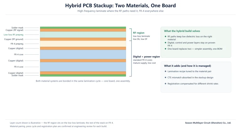
You rarely choose the package substrate — the chip vendor does, and the package datasheet fixes it. What you absolutely own is the host PCB’s job of receiving that package, and this is where substrate properties become board design constraints. A fine-pitch BGA on a BT substrate needs an escape-routing strategy that matches its ball pitch; a low-loss package interface is wasted if the first centimeter of board trace burns the margin with a cheap laminate; and a thermally demanding package needs copper planes and via stitching planned from the start.
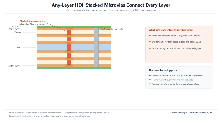
Concretely, three decisions matter most. First, stackup and materials: match the board dielectric to the speed of the interface leaving the package, as our laminate selection guide walks through. Second, via technology: breakout regions under dense BGAs usually need laser microvias rather than through-holes, which is the territory of HDI PCB technology. Third, impedance control: memory and RF interfaces expect the board to continue the impedance the substrate started, within stated tolerances rather than best effort.
A useful mental model is continuity: signal integrity, thermal path, and mechanical stress all cross from the substrate into the PCB without stopping at the ball array. Teams that treat the package as the chip vendor’s problem and the board as their own tend to discover the gap during qualification, when changes are expensive. Teams that review the two together — substrate datasheet in one hand, board stackup in the other — catch the mismatches on paper.
BT Substrate Selection Checklist for Buyers
For procurement engineers, the useful checklist is short and can be run before any quote is requested. It separates what the chip vendor has already decided from what still needs a decision, and it prevents the two most common sourcing surprises: a board that cannot escape-route the package, and a bill of materials that quietly assumes capabilities nobody confirmed.
- Confirm the package substrate class from the chip vendor’s datasheet — BT-class, ABF-class, or ceramic — and record it in the BOM notes.
- Extract the ball pitch and ball array from the package drawing and verify your board’s escape strategy (dog-bone, via-in-pad, or routed) against your fabricator’s capability.
- Check reflow profile compatibility: the substrate Tg is fixed, but your board laminate Tg must survive the same assembly process.
- Define impedance targets for every interface leaving the package, with tolerances, instead of leaving them to default.
- Confirm surface finish on the board side (ENIG, OSP, or HASL) against the package balls’ solderability requirements.
- Agree the acceptance standard — IPC Class 2 or Class 3 — before quoting, since it changes both yield expectations and price.
None of these items requires substrate-level expertise; they require the habit of reading the package datasheet as a board-level input. The checklist also doubles as a good set of questions to put to any prospective board supplier, because the quality of the answers tells you quickly whether the supplier engineers the stackup or just copies it.
Common BT Substrate Specification Mistakes
The most frequent mistake is treating the package substrate as a line item to be value-engineered. Unlike the host board, the substrate is inseparable from the chip vendor’s qualification: swapping it invalidates the package’s reliability data, and no cost saving survives that trade. The second mistake is the mirror image — over-specifying — where teams specify ABF-class features for memory-class needs and pay a multiplier that the application never justifies.
A third mistake shows up at the board interface: designs that copy the mechanical footprint of a package without checking the breakout region, then discover at layout time that a through-hole field cannot escape the ball array. That failure has nothing to do with the substrate itself and everything to do with not translating package geometry into board constraints early. The fix is procedural, not technical — put the package drawing and the substrate datasheet into the design review, and assign someone to own the interface explicitly.
Frequently Asked Questions
What is a BT substrate?
A BT substrate is an IC package substrate built on bismaleimide triazine (BT) resin reinforced with glass cloth. It redistributes a silicon die’s connections to a BGA footprint and provides heat dissipation and mechanical support. Typical properties include Tg of 170–220 °C, Dk of 3.4–4.2, and Df of 0.008–0.012, making it the dominant substrate class for memory, RF, and MEMS packages.
Is a BT substrate the same as a regular PCB?
No. Both are copper-clad laminates with similar process steps, but a package substrate works at semiconductor scale — line/space of tens of microns, much tighter registration, and semiconductor-style qualification — while a PCB carries the assembled packages at board scale. Most PCB factories, including capable HDI manufacturers, do not produce package substrates; they produce the boards the substrates mount onto.
Why is BT resin used in memory and RF packages?
Memory interfaces need hundreds of connections with low loss and tight CTE matching to silicon, and RF front-ends need low dissipation factor to preserve signal strength at high frequency. BT resin delivers Tg of 170–220 °C for assembly survival, CTE of 10–16 ppm/°C in-plane, and Df of 0.008–0.012 — the specific combination those applications need at a cost ABF-class materials cannot reach.
How does a BT substrate compare with an ABF substrate?
ABF substrates use a photo-imageable build-up film that supports line/space below 10 µm and the tall stacks processors need, at roughly 1.5–2 times the material cost of BT. BT substrates cover 25–80 µm line/space in volume production and dominate memory, RF, and MEMS packaging. In short: ABF for CPUs, GPUs, and AI accelerators; BT for everything density- and cost-balanced.
Can a standard PCB factory manufacture BT substrates?
Generally no — package substrate manufacturing is a specialty with semiconductor-grade registration, plating, and qualification requirements, and it is a different business from PCB fabrication. What a strong PCB partner does provide is the board that receives the BT-packaged chip: HDI breakout, controlled impedance, and matching laminate performance. If your project needs IC substrate supply, plan it through the chip vendor’s qualified substrate sources.
Does the package substrate affect my PCB design?
Yes, in three practical ways. The ball pitch and array determine your escape-routing and via strategy. The package’s electrical performance sets the impedance and loss targets your board must continue. And the package’s thermal behavior drives your copper weighting, via stitching, and airflow assumptions. Reading the package and substrate datasheets during stackup design avoids most of the surprises.
How much does a BT substrate cost?
IC substrates are priced through chip and package channels rather than quoted per square meter, so the useful frame is relative: BT-class material is the volume baseline for package substrates, ABF-class film typically costs around 1.5–2 times more, and polyimide more again. For the host PCB that carries the package, cost drivers are layer count, materials, line/space, and surface finish — confirmed at engineering review, not before.
Designing the Board That Carries Your BT-Packaged Chips?
If your product uses memory, RF, or MEMS packages, the host PCB has to continue what the BT substrate started — impedance, thermal path, and breakout density. Our PCB manufacturing services cover 2–30 layer boards with HDI microvias and controlled impedance for exactly these designs. Send us your Gerber files for an engineering review, and our PCB materials and laminates guide can help you pick the right stackup before you commit.