Book Appointment Now

What an AI server PCB demands: layer counts, low-loss laminates, power delivery, thermal design, and the manufacturing features behind accelerator boards.
AI Server PCB: The Technical Requirements Behind Accelerator Boards
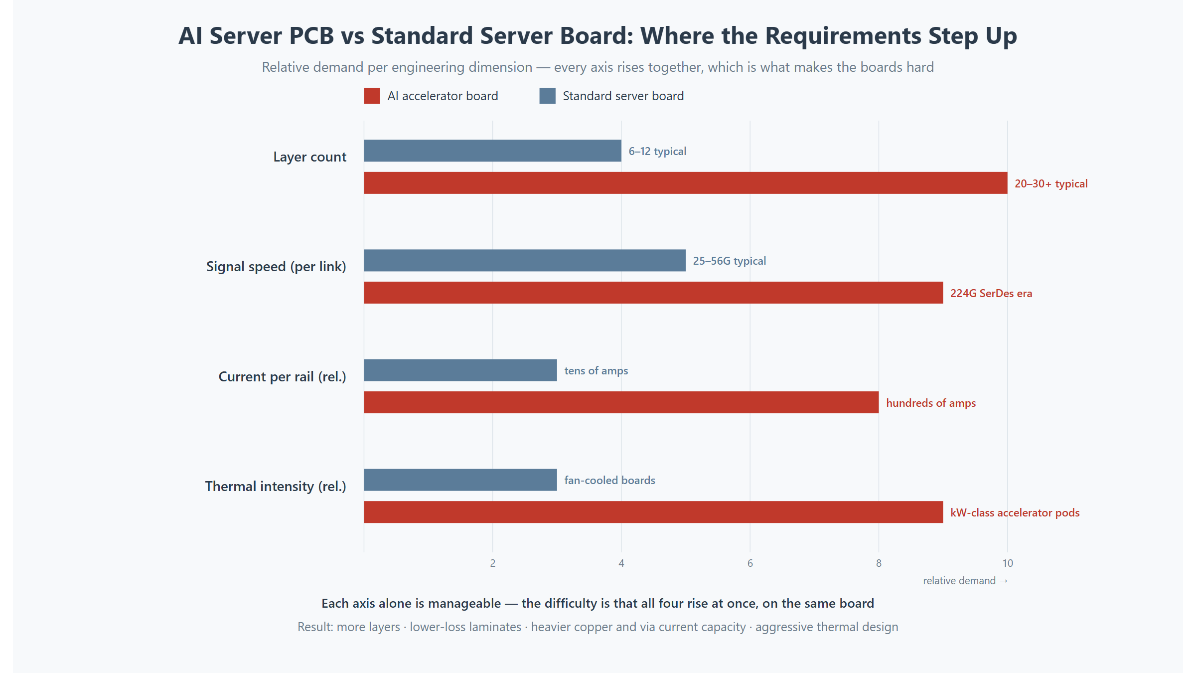
An AI server PCB is not a server board with more copper — it is a different engineering problem. Accelerator boards carry 20–30+ layers, per-link speeds an order of magnitude beyond conventional designs, power rails measured in hundreds of amps, and thermal loads dominated by dies that dissipate like small space heaters. The chart above tells the story: each requirement axis steps up at the same time, and that combination is what makes these boards hard.
This guide walks through the technical requirements dimension by dimension — structure, materials, signal integrity, power delivery and thermal design — and closes with the manufacturing features (back-drilling, heavy copper, tight registration) that turn the design into a buildable board. The cost side of the same story is covered separately in our AI server PCB cost drivers guideGlobal Electronics Association standards library.
Table of Contents
- What Makes an AI Server PCB Different
- Layer Counts and Board Size: The Structural Baseline
- Low-Loss Laminates: The Material Selection
- Signal Integrity at Accelerator Speeds
- Power Integrity: Feeding Hundreds of Amps on an AI Server PCB
- Thermal Design for Dense Accelerator Boards
- Manufacturing Features: What These Boards Ask of the Fabricator
- Specifying an AI Server Build: What to Send and What to Ask
- FAQ
- Planning an Accelerator or High-Layer-Count Build?
What Makes an AI Server PCB Different
Three load categories define the difference between an accelerator board and a standard server board:
- Data movement. Accelerator interconnects — chip-to-chip, board-to-board, rack-to-rack — run at speeds where every via, connector transition and plane split is an electrical event. The board is the transmission-line system.
- Power delivery. Modern accelerator dies draw hundreds of amps at sub-volt rails. Delivering that current with acceptable ripple turns the board’s copper layers into part of the power supply.
- Heat. kW-class modules concentrate dissipation that conventional boards spread across an enclosure. The board participates in the thermal path whether designed to or not.
A standard server board optimizes these one at a time. An AI server PCB has to solve all three simultaneously on the same stackup — which is why the requirements interact, and why trade-offs made in isolation show up as failures elsewhere.
Layer Counts and Board Size: The Structural Baseline
Layer count in accelerator land is not a routing convenience — it is driven by three non-negotiable needs:
- Escape and breakout. Large flip-chip packages with thousands of pins need escape layers that conventional boards never approach; 20–30+ layer builds are the working norm for flagship accelerator carriers.
- Reference plane density. Every high-speed layer pair needs clean reference planes, and power delivery wants its own plane pairs per voltage domain — planes consume layers as fast as signals do.
- Copper mass. Hundreds of amps per rail need wide, thick, often multiple-layer copper infrastructure; 2–3 oz internal planes are common where 1 oz is the server-board default.
Board size grows with the layer count: larger panels carry the accelerator sockets, memory channels and connector fields, and thicker finished boards (2.4 mm and beyond on 20+ layer builds) follow from the copper mass. Thickness interacts with via technology — longer barrels mean longer stubs, which is where back-drilling enters the conversation later in this guide. The stackup-ordering principles that keep these tall stacks symmetric and manufacturable are in our stackup design guide.
Low-Loss Laminates: The Material Selection
Material selection is the biggest single material-cost decision on the board, and it is set by loss, not by Dk:
| Loss tier (Df at ~10 GHz) | Material class | Typical fit on AI server builds |
|---|---|---|
| ≈ 0.020 (mid-loss) | Improved FR-4 / mid-tier systems | Power layers, lower-speed management nets; cost control on non-critical layers |
| ≈ 0.008–0.012 (low loss) | Low-loss glass systems | Most high-speed routing layers on mainstream accelerator boards |
| ≈ 0.003–0.005 (ultra low loss) | Premium PTFE-family / hydrocarbon systems | The fastest nets — top SerDes tiers and long chip-to-chip routes |
| Hybrid stackups | Premium only where needed | The standard cost answer: ultra-low-loss layers for critical nets, mid-loss elsewhere |
Hybrid construction — mixing laminate grades within one stackup — is how AI server boards keep material cost proportional to performance. The mechanics and cautions of mixed-dielectric builds are covered in our hybrid stackup guide, and the selection framework across grades in our laminate selection guide.
Two selection realities worth remembering: material datasheet loss is measured under lab conditions and varies with resin content and glass style per layer, and the glass-style/resin interactions that matter for reliability — CAF resistance among them — are detailed in our prepreg selection guide.
Signal Integrity at Accelerator Speeds
At multi-gigabit-per-link speeds, the signal-integrity playbook tightens from ‘good practice’ to ‘non-negotiable’: every layer transition is engineered, every stub is budgeted, and every reference-plane discontinuity is designed out before routing starts. The complete framework — reflections and terminations, return paths, crosstalk levers — is in our signal integrity framework guide. Three items dominate specifically on accelerator boards:
- Back-drilling. Through-vias on thick 20+ layer boards carry long stubs; removing the unused barrel is standard practice on the fastest net classes, with residual stub length specified on the fabrication drawing — the technique and limits are in our back-drilling guide.
- Impedance discipline at tight tolerance. Single-ended 50 Ω and differential 90–100 Ω are the routine targets, held to ±10% standard and tighter where the link budget demands; verification runs on the production coupon, as described in our impedance measurement guide.
- Connector and cable interface engineering. The board ends at a connector that must carry the same impedance discipline — pad geometry, antipad design and the local layer transition around every high-speed pin are engineered as one structure with the connector vendor’s footprint.
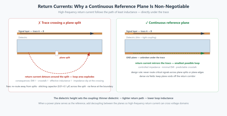
The unifying discipline is the reference plane: continuous, uninterrupted return corridors under every critical net. On a board with this many planes, power domains, and via fields, protecting those corridors is a full-time layout constraint — not a final check.
Power Integrity: Feeding Hundreds of Amps on an AI Server PCB
Power delivery is where AI server boards diverge most visibly from conventional designs. A single accelerator rail drawing hundreds of amps at sub-volt output turns milliohms into meaningful voltage drop and micro-ohms of plane inductance into ripple:
- Copper infrastructure. Multiple plane layers dedicated to power and ground, heavy copper weights on those layers, and via stitching that treats power via farms as designed conductors rather than routing leftovers.
- PDN design as a system. The target impedance profile across frequency is engineered with the VRM, plane capacitance and decoupling network together; a plane pair’s natural capacitance and its resonances are part of the design, not an accident.
- Loss accounting. Every milliohm in the delivery path is dissipated as heat and subtracted from the rail margin — copper thickness on power layers is a thermal decision as much as an electrical one.
- Domain separation. Multiple voltage domains on one board reference different plane pairs; the return-path rules for signals crossing domains mirror the signal-integrity discipline above.
The copper-weight mechanics behind these choices — what 2 oz, 3 oz and heavier planes actually deliver — are laid out in our heavy copper design rules guide.
Thermal Design for Dense Accelerator Boards
Thermal design on an AI server PCB is constrained by an inconvenient fact: the heat sources are the same packages that demand the signal integrity. Every thermal feature competes for layers, space and copper with every electrical one. The working strategies, in the order they usually get deployed:
- Board-level conduction. Filled thermal via arrays under hot devices tie into internal planes that spread heat toward the board edge or module lid — the via and plane mechanics are in our thermal management guide.
- Copper as spreader. The same heavy power planes that feed hundreds of amps double as lateral heat spreaders; plane connectivity planning serves both masters.
- Material margin. Glass transition and decomposition margins keep the laminate stable through the thermal cycles that dense operation produces; laminate-grade context is in the laminate selection guide.
- Interface to the cooling system. The board’s exit paths — lid contact areas, mounting zones, edge conduction — are designed with the module’s cooling architecture, not after it.
The design-order point matters most: thermal, power and signal features claim the same layers. Sequencing their allocation during stackup definition — not during routing — is what keeps a dense accelerator board buildable.
Manufacturing Features: What These Boards Ask of the Fabricator
Translating the requirements above into a buildable board pulls a specific capability list:
| Feature | Why accelerator boards need it | Capability conversation |
|---|---|---|
| 20–30+ layer lamination | Escape, planes and copper mass all demand layer count | Registration capability at high layer counts; press symmetry |
| Back-drilling | Stub removal on thick stacks for multi-gigabit nets | Residual stub control and drill-to-copper accuracy |
| Heavy internal copper (2–3 oz) | Power rails and heat spreading on plane layers | Etch and plating consistency at weight, layer-pair registration |
| Hybrid laminate press | Premium material only on the layers that need it | Bond compatibility between dissimilar prepreg systems |
| Tight impedance tolerance | Link budgets at the fastest SerDes tiers | Coupon-based verification and per-layer impedance reporting |
| Large-panel handling | Accelerator carriers run big and thick | Panel size capability, warpage control, handling tooling |
Reliability closes the loop: these boards run hot, biased and loaded for years, so the laminate system’s cycling and CAF behavior matter at a level consumer boards never probe — the test context is in our reliability testing guide. The economics of all these features — what each one does to the quote — are analyzed in the companion cost drivers guide.
Specifying an AI Server Build: What to Send and What to Ask
Accelerator boards reward early engineering alignment. The data package that gets a useful quotation:
- Stackup intent — layer count, the net classes per layer, target impedances with tolerances, and the voltage domains with their current levels.
- Material intent — the loss tier per layer or the request to propose a hybrid stackup against the net-speed map.
- Special-process list — back-drill classes and residual stub budgets, via fill under BGAs, heavy copper planes, via-in-pad sites.
- Thermal interfaces — where the board meets the cooling system, and any copper features reserved for conduction.
- Verification expectations — which nets get coupon testing, what impedance reporting accompanies the lot, and the reliability test basis if specified.
The engineering review that follows should close the loop on feasibility layer by layer — plane connectivity, registration margins at the copper weights, hybrid-press compatibility — before the quote rather than after the first pilot fails. For the earlier rung of the server-board ladder, the structural comparison with conventional boards is in our backplane design guide.
Frequently Asked Questions
How many layers does an AI server PCB typically have?
Mainstream accelerator carriers run in the 20–30+ layer range, driven by package breakout density, reference-plane needs and the copper mass for power delivery. Management and support boards within the same server use conventional 8–14 layer builds.
Why do AI server boards need low-loss laminates?
At the per-link speeds accelerator interconnects run, laminate loss tangent — not conductor resistance — dominates signal attenuation over the route lengths involved. Lower-Df materials keep the eye open at the receiver; hybrid stackups apply premium material only to the layers carrying the fastest nets.
What is back-drilling and why is it standard on accelerator boards?
Back-drilling removes the unused portion of a through-via barrel beyond the layer where the signal connects. On thick 20+ layer boards that stub acts as a resonant antenna at multi-gigabit speeds. Residual stub length is specified on the fabrication drawing and verified on cross-section.
How is power delivery handled for hundreds-of-amp rails?
With dedicated heavy-copper plane pairs per voltage domain, via stitching farms designed as conductors, and a PDN engineered across frequency with the VRM and decoupling network. Plane thickness is chosen for both milliohm budget and heat spreading.
Can hybrid stackups mix laminate grades in one board?
Yes — and it is the standard cost answer for AI server boards: ultra-low-loss material on the fastest layers, mid-loss systems elsewhere. The cautions are press compatibility between prepreg systems, CTE matching across the stack, and registration behavior of the mixed construction.
What impedance targets and tolerances are typical?
Single-ended 50 Ω and differential 90–100 Ω are the routine targets. Tolerance is ±10% as the standard control, with tighter control available where link budgets demand it — feasibility is confirmed against the actual stackup at engineering review and verified on production coupons.
How does thermal design coexist with signal routing on the same board?
By allocating layers at stackup definition time: filled thermal via arrays, heavy spreading planes and conduction zones claim their layers before high-speed routing is assigned. The heat sources and the signal integrity both concentrate under the same packages, so sequencing — not afterthought patching — is the workable method.
What should I submit for a first quotation on an accelerator board?
Stackup intent (layers, net classes, impedance targets), material tier per layer or a request for a hybrid proposal, the special-process list (back-drill classes, via fill, heavy copper), thermal interfaces, and the verification expectations. A quotation built on that package reflects the real build rather than a generic per-layer price.
Planning an Accelerator or High-Layer-Count Build?
Send your layer plan, net-speed map and power-rail requirements, and our engineering team will review the stackup, hybrid-material options, back-drill budgets and heavy-copper feasibility before quotation. Production runs from 2 to 30 layers (up to 64 layers for prototypes, subject to per-order review), with process feedback typically the same day.
Season PCB direct: Tel (+86) 18681528532 | WhatsApp +86 18681528532
E-mail: roc@season-pcb.com