Book Appointment Now

12-Layer 2-Stage HDI Rigid Flex PCB Manufacturer
As an IPC Class 3 rigid flex PCB manufacturer, Season PCB bonds rigid FR-4 circuit sections and a polyimide flexible core into one laminated structure, eliminating the board-to-board connectors and cable assemblies that fail first under shock and vibration. This rigid-flex PCB product family page covers our 12-layer 2-stage HDI rigid flex PCB build. It pairs a 2+8+2 stackup on high-Tg FR-4 with 0.10 mm laser blind vias, 2.8/2.5 mil line and space, 0.25 mm BGA support and ENIG, quoted and built to IPC-6013 Class 3.
Every board from this rigid flex PCB manufacturer is laminated in two sequential HDI cycles over a buried-via core. X-ray registration and coupon testing between the cycles catch process drift at the layer level. Prototype and volume production run on the same qualified lines across three plants, and each order ships with impedance coupon data, E-test reports, micro-section photographs and a certificate of conformance.
Send Gerber RS-274X or ODB++ data with your stackup and bend-zone drawing for a DFM review and quotation, typically within 24 hours. If your program also needs a rigid 2-stage HDI platform, the 12-layer 2-stage HDI core board covers the rigid-only equivalent on the same process.
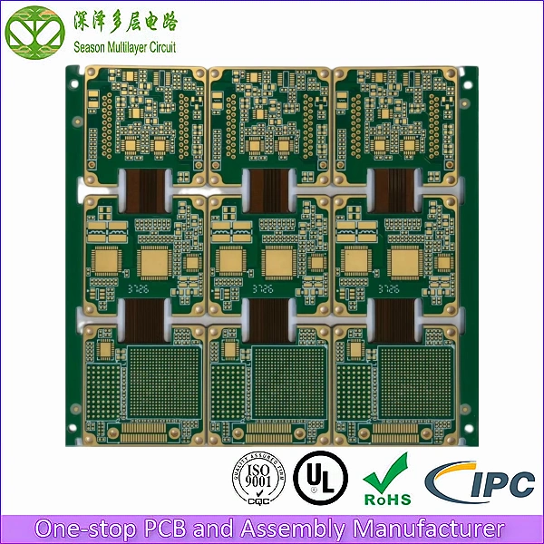
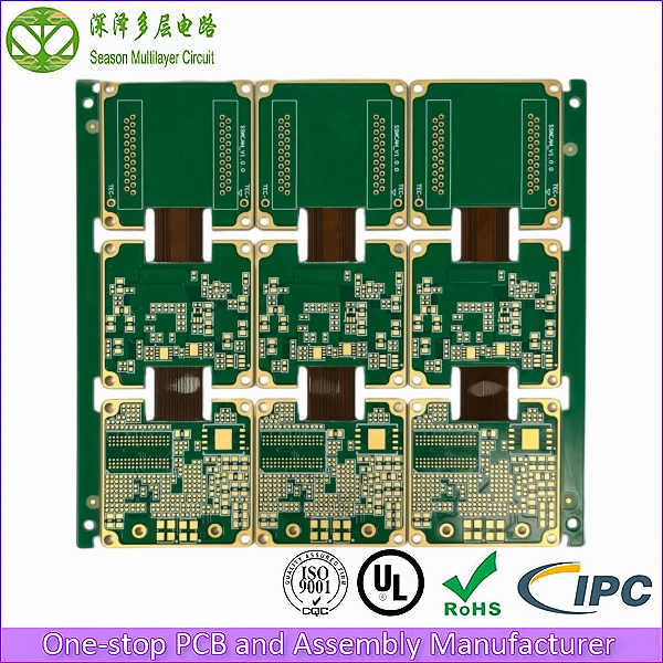
2+8+2
Build-Up Stackup
0.10 mm
Min Laser Blind Via
0.25 mm
Min BGA Pitch
±10%
Impedance Control
ENIG1-2µ”
Surface Finish
ISO9001-2004
ISO14001
UL (E305905)
IPC-Class 2/Class 3
IATF 16949
RoHS
What a 12-Layer 2-Stage HDI Rigid-Flex PCB Is
A 12-layer 2-stage HDI rigid-flex PCB permanently bonds rigid FR-4 circuit sections to a polyimide flexible circuit core in one laminated structure, so the interconnect folds into the enclosure instead of being patched together from boards, ribbon cables and connector pairs. A rigid flex PCB manufacturer has to control both lamination cycles and the flex transition in-house to make that claim; this page shows how we do both.
The 2-stage HDI designation, also written as second-order or 2+N-2 HDI, means two sequential laser microvia build-up cycles on each outer side of the rigid-flex core. Signal layers connect through stacked microvias across multiple dielectric layers. The via mechanics behind this build are explained step by step in our HDI PCB technology guide.
In the standard 12-layer build, a symmetrical 2+8+2 stackup places two HDI build-up layers on each side of the rigid-flex core. Laser-drilled microvias as small as 0.10 mm link L1 to L3 and L10 to L12, while mechanically drilled through-vias stitch the flex core to the rigid sections. Every layer pair is registered, laser-drilled, copper-filled and planarized under one controlled lamination sequence. The result is measurably lower interconnect resistance and better high-frequency signal integrity than a two-piece assembly delivers, which is why reliability-driven OEMs write the rigid flex PCB build into the drawing rather than the appendix.
The lighter alternative in the same family is the 6-layer rigid-flex PCB, which shares the same flex-to-rigid transition discipline at a lower layer count. This page focuses on the 12-layer 2-stage HDI platform for dense control, computing and instrumentation electronics.
Why a Rigid-Flex PCB Replaces Rigid Boards and Cable Assemblies
Most programs arrive at rigid-flex after a rigid-board-plus-cable architecture has failed in one of three ways: a connector opened up under vibration, the cable harness consumed the remaining enclosure volume, or assembly labor cost more than the boards. The comparison below is the one we walk through with engineering teams during DFM review.
| Factor | Rigid Boards + Flex Cable + Connectors | 12-Layer 2-Stage HDI Rigid-Flex PCB |
|---|---|---|
| Interconnect joints | Every cable adds 2–4 connector mate points per end | Zero separable joints across the assembly |
| Vibration survival | Limited by the weakest connector latch | Copper is continuous from L1 to L12 |
| Assembly labor | Cable routing, dressing and torque steps per unit | One placement, one reflow profile |
| Packaging volume | Connector bodies and bend clearance add 5–15 mm | Folds to the enclosure geometry |
| Signal integrity | Impedance discontinuity at every transition | Controlled impedance end to end, ±10% (tighter by layer) |
| Traceability | Three vendors, three quality systems | One build record, one Class 3 acceptance package |
| Unit cost at volume | Lower board cost, higher assembly and field-failure cost | Higher board cost, lower total installed cost |
The economics typically cross over once a design carries more than two cable assemblies or ships into a shock and vibration environment, which describes most of the high-reliability industrial rigid flex PCB work we build.
2-Stage vs 1-Stage HDI: When the Second Stage Pays Off
Not every rigid flex PCB needs a second lamination cycle. The honest answer we give customers: 1-stage is the right tool below a certain density threshold, and paying for 2-stage below it is waste. The table below frames the decision.
| Attribute | 1-Stage HDI (1+N-1) | 2-Stage HDI (2+N-2) |
|---|---|---|
| Microvia reach | L1 to L2 only | L1 to L3 stacked (or staggered) |
| BGA breakout | Comfortable at 0.5 mm pitch and above | Routable at 0.25–0.4 mm pitch |
| Routing density | Standard HDI density | Substantially higher escape density in rigid zones |
| Lamination cycles | One | Two, with resin plug + planarization between |
| Typical use | Wearables, consumer modules, mid-density automotive | High-density computing, instrumentation, test and measurement |
| Relative cost | Base | Premium justified by density or layer escapes |
On a 12-layer platform the second stage is usually worth it: eight core layers already put a 12-layer rigid flex PCB in high-density territory, and 0.25 mm pitch BGA breakout in the rigid zones is the norm on this class of hardware. If your device sits below that threshold, our 12-layer 1-stage HDI PCB page covers the lighter alternative on the same qualified lines.
Technical Specifications of the 12-Layer 2-Stage HDI Rigid-Flex PCB
The table below is the capability envelope this rigid flex PCB manufacturer quotes against for the platform. Values marked as options are confirmed at engineering review against your Gerber data.
| Parameter | Specification | Notes |
|---|---|---|
| Layer count | 12 layers, 2-stage HDI (2+8+2 build-up) | Two laser stages per side, mirrored |
| Base material | High-Tg FR-4 rigid zones + adhesiveless polyimide FCCL flex zone | Tg 170 °C, Td > 340 °C; Isola, Rogers, DuPont Pyralux, Shengyi |
| Min laser blind via | 0.10 mm | Stacked or staggered, L1-L3 / L10-L12; plugged or filled |
| Min through via | 0.20 mm | Through L1-L12 across rigid and flex zones |
| Line / space | 2.8 / 2.5 mil | Inner layers tuned per impedance model |
| Min BGA pitch | 0.25 mm | Via-in-pad with plugged and filled microvias |
| Copper weight | 1 oz (35 μm) outer, 0.5 oz (18 μm) inner | Heavy copper power layers as option |
| Impedance control | ±10% standard; ±8% and ±5% by layer | Per-panel TDR coupon against the impedance model |
| Minimum bend radius | 6× flex thickness (static), per IPC-2223 | Bend coupon validated on every Class 3 build |
| Surface finish | ENIG 1–2 µ” | OSP, immersion silver, hard gold body on request |
| Solder mask / coverlay | LPI solder mask on rigid zones; polyimide coverlay on flex zones | Customer-specified color; matte or gloss |
| Silkscreen | Epoxy ink, customer-specified | Single or both sides |
| Acceptance standard | IPC-6013 Class 3 · IPC-A-600 Class 3 | Full acceptance documentation package per lot |
| Quality system | ISO 9001:2015 · IATF 16949 | UL recognized laminate systems, RoHS & REACH |
Final rigid flex PCB parameters are confirmed per drawing during DFM review. For the rigid-only equivalents of this platform, see the 12-layer 2-stage HDI core board.
The 2+8+2 Stackup and Flex Zone Construction
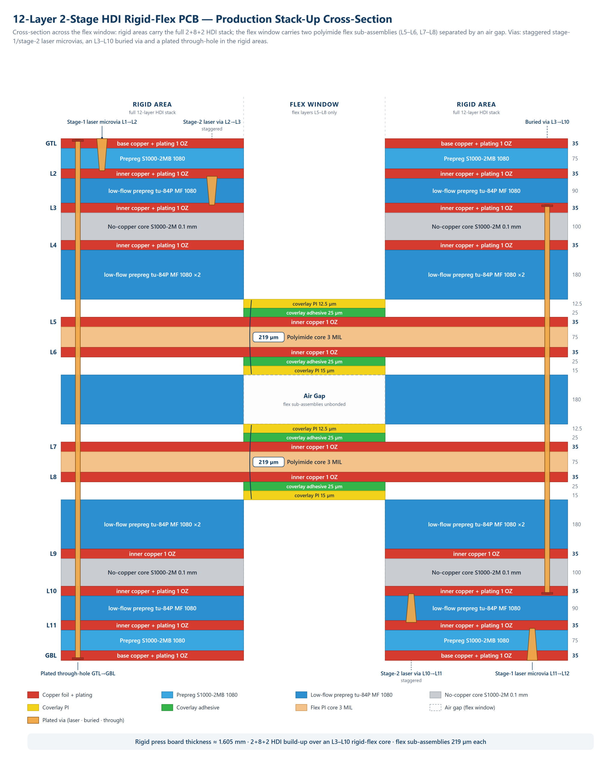
The symmetrical 2+8+2 construction balances copper and dielectric distribution across the board centerline, keeping warpage inside Class 3 limits through both lamination cycles. Each stage adds one laser-drilled, copper-filled microvia layer to the outer faces of the eight-layer rigid flex PCB core; buried vias in the L3–L10 window are resin plugged at cycle 1.
Exact dielectric thicknesses, copper weights and via structures are defined per rigid flex PCB design in the engineering build-up file issued for approval before tooling.
- L1 / L12 outer build-up — second HDI stage: laser-drilled 0.10 mm microvias, copper filled and planarized before outer foil lamination.
- L2 / L11 build-up stage 1 — first laser cycle over the core, giving stacked L1→L3 and L10→L12 interconnects.
- L3–L10 buried-via core — the eight-layer rigid-flex core on high-Tg FR-4 with adhesiveless polyimide through the flex window; buried vias resin plugged at cycle 1.
- Flex zone layer continuation — a subset of layers continues through the flex window (typically the power/ground pair and dedicated flex signal layers), while rigid-only layers terminate at the transition. Selective continuation keeps the bend zone flexible without cutting signal returns.
- Through-hole stitching — mechanically drilled 0.20 mm through-vias anchor the flex core to both rigid sections outside the bend radius.
- Coverlay and stiffeners — polyimide coverlay with rounded openings protects the flex zone; FR-4 or PI stiffeners are added where connectors or zero-clearance mounting demand local rigidity.
Impedance Control Plan Across the Rigid Stack and Flex Section
The impedance model defines every controlled structure on this rigid flex PCB layer by layer: single-ended 39 Ω and 50 Ω lines in the rigid stack, 76 Ω and 100 Ω differential pairs, and two structures continuing through the flex (FPC) section. Columns under Original Design show the trace geometry as received from the customer; the Adjusted columns are the production geometry after tuning each layer against the stackup model. All trace values are in mils. Coupon traces built to this plan are measured by TDR at Gate 3 of the inspection flow before any rigid flex PCB batch ships.
| Controlled Layer | Type | Reference Layer | Impedance (Ω) | Tolerance (Ω) | Original Design | Adjusted | |||||||
|---|---|---|---|---|---|---|---|---|---|---|---|---|---|
| Original Width (mil) | Original Spacing (mil) | Original to Plane (mil) | Adjusted Width (mil) | Adjusted Spacing (mil) | Adjusted to Plane (mil) | ||||||||
| L1&L12 | Single-ended | L2 / L11 | 50 | ±5 | L2 / L11 | 50 | ±5 | 4.5 | 4.5 | ||||
| L3&L10 | Single-ended | Default | 50 | ±5 | Default | 50 | ±5 | 3.4 | 3.6 | ||||
| L5&L8 | Single-ended | Default | 50 | ±5 | Default | 50 | ±5 | 3.4 | 3.5 | ||||
| L1&L12 | Single-ended | L2 / L11 | 39 | ±5 | L2 / L11 | 39 | ±5 | 7.1 | 7.2 | ||||
| L3&L10 | Single-ended | Default | 39 | ±5 | Default | 39 | ±5 | 3.9 | 4.4 | ||||
| L5 | Single-ended | L4 / L6 | 39 | ±5 | L4 / L6 | 39 | ±5 | 3.9 | 5.7 | ||||
| L12 | Differential | L11 | 76 | ±7.6 | L11 | 76 | ±7.6 | 6.5 | 5 | 6.2 | 5.3 | ||
| L3&L10 | Differential | Default | 76 | ±7.6 | Default | 76 | ±7.6 | 4 | 8.9 | 4.4 | 8.5 | ||
| L5 | Differential | L4 / L6 | 76 | ±7.6 | L4 / L6 | 76 | ±7.6 | 4 | 8.9 | 5.6 | 7.3 | ||
| L1&L12 | Differential | L2 / L11 | 100 | ±10 | L2 / L11 | 100 | ±10 | 4.1 | 8.8 | 4 | 8.9 | ||
| L3&L10 | Differential | Default | 100 | ±10 | Default | 100 | ±10 | 3.2 | 9.7 | 2.5 | 10.4 | ||
| L5&L8 | Differential | Default | 100 | ±10 | Default | 100 | ±10 | 3.2 | 9.7 | 3.3 | 9.6 | ||
| Flex (FPC) section | |||||||||||||
| L5&L8 | Single-ended | Default | 50 | ±5 | Default | 50 | ±5 | 6.3 | 5.8 | ||||
| L5&L8 | Differential | Default | 100 | ±10 | Default | 100 | ±10 | 5.2 | 7.7 | 4.9 | 8 | ||
What Makes This 12-Layer 2-Stage HDI Rigid-Flex PCB Exceptional
12 Layers, 2+8+2 Build-Up
Two laser stages per side over an eight-layer rigid-flex core, mirrored around the centerline to keep warpage inside Class 3 limits through both lamination cycles.
0.10 mm Laser Blind Vias
Stacked or staggered from L1 to L3 and L10 to L12, laser-drilled, copper-filled and planarized before the next stage runs.
0.25 mm BGA Breakout
Via-in-pad with resin-plugged, copper-capped microvias makes fine-pitch escapes routable in the rigid zones of the rigid flex PCB.
2.8/2.5 mil Line and Space
Inner layers tuned per the impedance model for dense control, computing and instrumentation layouts.
±10% Impedance Control
Standard ±10%, with ±8% and ±5% available by layer, verified with a TDR coupon on every panel.
Adhesiveless Polyimide Flex Core
12.5–25 μm polyimide FCCL with no adhesive layer to creep or fatigue in the bend zone of the rigid flex PCB.
−55 °C to +150 °C Materials
High-Tg FR-4 rigid zones with Td > 340 °C, qualified through both lamination cycles for industrial electronics.
IPC-6013 Class 3 Acceptance
Every rigid flex PCB is built and accepted to IPC-6013 Class 3, with a full documentation package per lot.
Design Rules for 12-Layer 2-Stage HDI Rigid-Flex That Prevent Respins
Most rigid flex PCB respins trace back to four design decisions made before the first quote. Building these into your layout from the start keeps the DFM review short and the yield predictable.
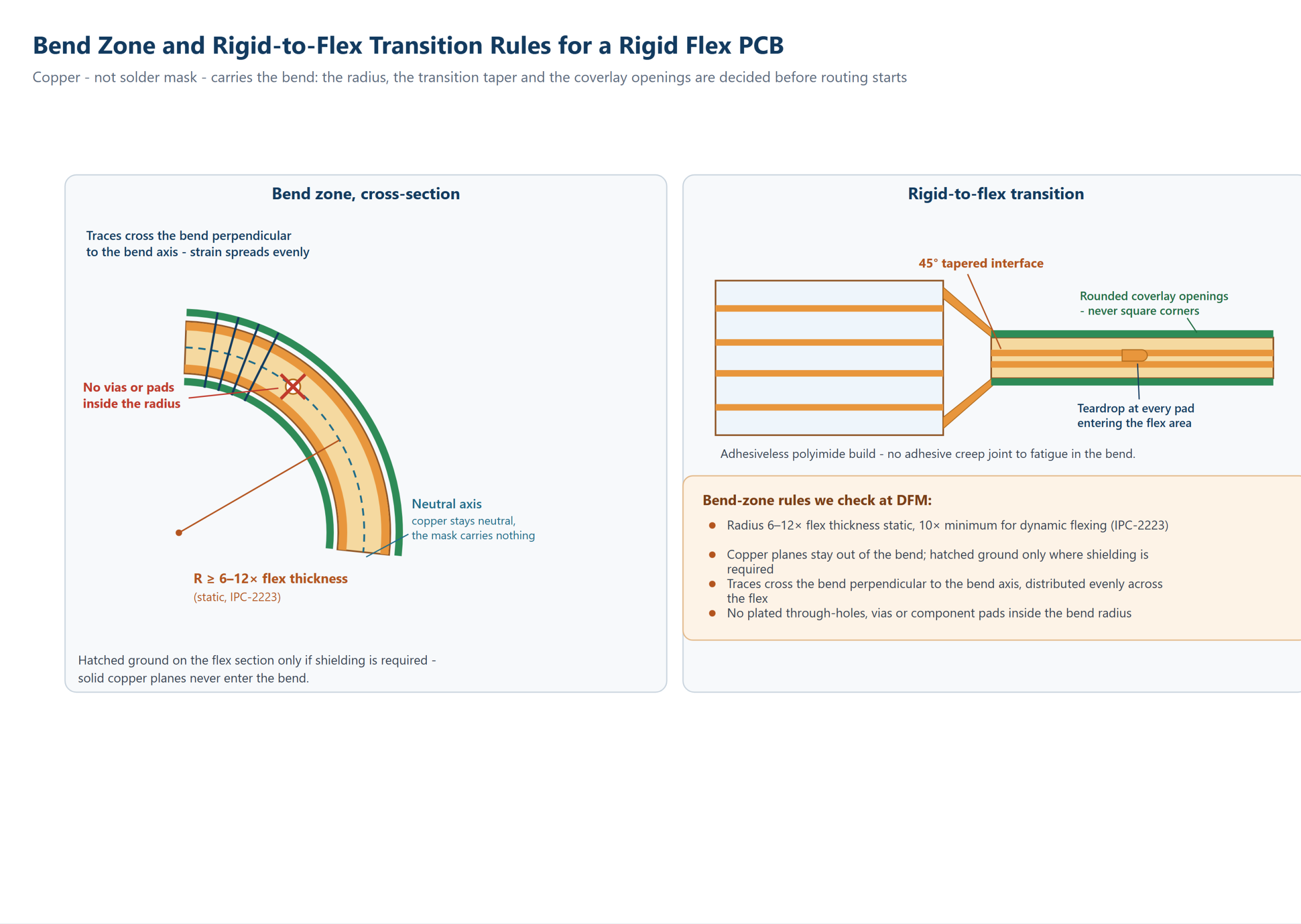
Bend Zones: Copper, Not Solder, Carries the Load
Route traces perpendicular to the bend axis only where unavoidable; traces crossing a flex zone parallel to the bend direction distribute strain evenly and survive orders of magnitude more cycles. Keep copper planes out of the bend area entirely, with hatched ground on the flex section if shielding is required. Never place plated through-holes, vias or component pads inside the radius. Per IPC-2223, size the radius at 6–12× total flex thickness for static bends and at least 10× for dynamic flexing. The IPC standards library is the reference point for the full acceptance criteria.
Rigid-to-Flex Transitions: Ease the Strain
The transition zone is where stress concentrates. Use a 45° tapered interface instead of a straight boundary, add teardrops at every pad entering the flex area, and specify rounded coverlay openings rather than square ones. We build the transition with adhesiveless polyimide so there is no adhesive creep joint to fatigue — one of the reasons Class 3 programs accept the construction.
Via-in-Pad and Stacked Microvias
At 0.25 mm BGA pitch, via-in-pad with resin-plugged, copper-capped microvias is standard practice on this rigid flex PCB build, and the second HDI stage makes L1→L3 escapes routable. The reliability-critical parameter is planarization: each stage’s via fill must be flat before the next laser cycle, which is why dimple height is a tracked parameter in our six-gate inspection flow.
Impedance Across Two Materials
Polyimide’s Dk (about 3.4) differs from FR-4 (about 4.2–4.5), so a differential pair tuned in the rigid zone detunes as it crosses into flex unless the stackup compensates. Give us your impedance targets per net class; we model both zones of the rigid flex PCB, adjust dielectric and copper geometry, and verify the result with a TDR coupon on every panel.
Materials That Hold Up from −55 °C to +150 °C
Material selection on a 12-layer 2-stage HDI rigid flex PCB is a CTE-management problem as much as an electrical one: FR-4 and polyimide expand at different rates, and the lamination sequence has to absorb that mismatch twice. The table below shows the material roles we assign by default; the full selection logic is covered in our PCB materials and laminates guide.
| Zone / Role | Default Material | Why It Is Chosen |
|---|---|---|
| Rigid zone laminate | High-Tg FR-4, Tg 170 °C, Td > 340 °C | Lead-free reflow qualified, low Z-axis expansion, Class 3 proven |
| Flex zone core | Adhesiveless polyimide FCCL, 12.5–25 μm PI | No adhesive layer to creep or fatigue in the bend zone |
| HDI dielectric | Low-loss prepreg, laser-drillable | Clean CO2 laser ablation, stable Dk for ±10% impedance |
| High-speed option | Isola, Rogers, or Shengyi low-Dk systems | For high-frequency nets; Dk/Df per data sheet |
| Flex-zone shielding | Hatched crosshatch copper or specialized shield layers | EMI control without stiffening the bend zone |
| Coverlay | Polyimide film with adhesive, rounded openings | Flexible protection that distributes mechanical stress |
Program-specific requirements such as a mandated laminate list, a qualification test plan, or CTE targets for a large ceramic BGA are handled at stackup review for every rigid flex PCB program before lamination tooling is cut. DuPont Pyralux adhesiveless systems and Shengyi flex-grade materials are both in routine use on our lines.
Where the 12-Layer 2-Stage HDI Rigid-Flex PCB Is Deployed
As a rigid flex PCB manufacturer with two decades of multilayer production behind it, Season PCB builds this platform for products that combine extreme interconnect density with extreme reliability, in packages a rigid board plus cable assembly can no longer fit.
Industrial Automation and Robotics
Robot arm joints, moving gantries, machine-vision heads and automated guided vehicles: the interconnect must survive millions of flex cycles and constant vibration with zero connector failures. Folding a 12-layer rigid flex PCB around the joint geometry also removes the cable service loops that dominate the bill of materials.
Test, Measurement and Instrumentation
Semiconductor test heads, downhole logging tools and portable instrumentation pack dense computing into handheld or rack-mounted enclosures. The 2-stage HDI build-up breaks out fine-pitch processors in the rigid zones while the flex section of the rigid flex PCB absorbs the lid, hinge or drawer motion of the instrument.
Automotive and Mobility Electronics
Built under our IATF 16949 quality system, the platform fits cockpit displays, camera and sensor clusters, and lighting controllers where the electronics wrap around the housing. Zero separable joints remove the connector failures that dominate warranty returns on high-vibration platforms.
Our Quality Guarantee: Six Inspection Gates from Imaging to Packing
Gate 1: Automated Optical Inspection
After every imaging step, AOI verifies the 2.8/2.5 mil geometry on every rigid flex PCB layer before it moves on.
Gate 2: X-Ray Registration
Checks via fill level and rigid-to-flex registration across both lamination cycles.
Gate 3: TDR Impedance Coupon
A coupon on every rigid flex PCB panel is measured against the impedance model before the build is released.
Gate 4: Flying Probe and E-Test
The full netlist is compared against the Gerber source, and every board passes 100% electrical test with no sampling.
Gate 5: Micro-Section Analysis
Verifies microvia fill, barrel copper and plating bonds at the layer level, not at final inspection.
Gate 6: Packing Records
Impedance coupon data, E-test report, micro-section photographs and the certificate of conformance travel with every rigid flex PCB batch.
Every batch from our lines ships with its record package: impedance coupon data, E-test report, micro-section photographs and the certificate of conformance that audited customers expect from a Class 3 rigid flex PCB manufacturer. The full flow, from file review to packing, is described on our PCB manufacturing services page, and the equipment behind these numbers is listed on the manufacturing capability page.
From Gerber Data to Class 3 Delivery
Both lamination cycles of the rigid flex PCB are verified by X-ray registration and coupon testing before the next stage proceeds, so any process drift is caught at the layer level, not at final inspection.
- 1. DFM review — stackup, bend zones and yield check against your data package.
- 2. Core lamination — the eight-layer rigid-flex core is pressed with buried vias resin plugged.
- 3. HDI stage 1 — laser drill, copper fill and planarization of the first build-up.
- 4. HDI stage 2 — second build-up cycle, X-ray verified before outer foil lamination.
- 5. Finish and test — ENIG plating, TDR coupon measurement and 100% electrical test.
- 6. Final QC — micro-section, dimensional audit and the Class 3 acceptance package.
Why Choose Season PCB as Your Rigid Flex PCB Manufacturer
- HDI is an in-house core process. 1-stage, 2-stage and any-layer build-ups run on the same lines as standard multilayer work, so the lamination profile of your 2+8+2 rigid-flex never changes hands mid-build.
- Capacity behind the prototype. Part of 998PCB Group, manufacturing since 2006, with 3,000,000 m² of annual capacity across plants in Shenzhen, Jiangxi and Anhui, and a 2–30 layer range.
- Quality system built for audited programs. ISO 9001:2015 and IATF 16949 quality systems, IPC-6013 Class 3 build standard, IPC-A-600 Class 3 acceptance, UL recognized laminate systems, RoHS and REACH compliance — see our UL certified PCB standards overview.
- Engineering contact, not a ticket queue. The engineer who reviews your stackup and bend zones answers questions during fabrication.
- Turnkey option. Bare board, or board plus assembly — see PCB manufacturing services for how the two are split.
Two Decades of Multilayer Production
Season PCB has run 12-layer HDI and rigid flex PCB volumes since 2006 across three plants, on lines qualified for both lamination cycles.
2-Stage HDI at Production Yield
Buried-via cores, resin plug and planarization are controlled between the two cycles, so yield does not depend on heroics at final inspection.
Impedance Modeled in Both Zones
FR-4 and polyimide are modeled separately and verified with a TDR coupon on every panel of your rigid flex PCB build.
Class 3 Records with Every Batch
Impedance coupon data, E-test reports, micro-section photographs and a certificate of conformance ship with each lot.
Prototype and Volume on One Line
NPI builds and production volumes run on the same qualified rigid flex PCB process, so the design does not drift between prototype and ramp.
One-Stop PCB + PCBA
Component sourcing and SMT for the rigid sections run under the same quality system, described on our PCB manufacturing services page.
The group behind this rigid flex PCB platform — its plants, equipment and capability envelope — is profiled in our 998 PCB Group manufacturer overview.
What to Send for a Same-Week Rigid-Flex Quote
A complete data package is the single biggest accelerant for a Class 3 rigid flex PCB quotation. Here is the checklist our quoting engineers work from:
- 1. Circuit data — Gerber RS-274X or ODB++, with rigid and flex zones either separated by layer file or clearly marked on one drawing.
- 2. Stackup or build-up requirement — your target stackup, or just the constraints (total thickness, impedance targets, layer count) and we propose the 2+8+2 build-up.
- 3. Outline drawing — dimensioned outline showing rigid-to-flex transition locations, bend areas and radii, stiffener locations if any.
- 4. Impedance targets — net classes and values if controlled; we model rigid and flex zones separately because the Dk differs.
- 5. Acceptance class and quantity — IPC-6013 Class 3 as applicable, prototype quantity, and expected annual volume so the panelization is priced honestly.
- 6. Surface finish and material calls — ENIG is our default for Class 3; flag any mandated laminate or finish early.
Send the package to this rigid flex PCB manufacturer via the quote button above or email it directly — a complete package is quoted typically within 24 hours, and incomplete packages get specific questions back within the same window. For a deeper look at the variables that move a quotation, see the components of PCB prices.
Frequently Asked Questions
What does 2-stage HDI mean on a rigid-flex PCB?
2-stage HDI (also called second-order or 2+N-2 HDI) means two sequential laser microvia build-up cycles are formed on each side of the rigid-flex board. On a 12-layer 2+8+2 stackup, two build-up layers sit on each outer side of the rigid-flex core, enabling L1-to-L3 and L10-to-L12 microvia interconnects with stacked or staggered via structures.
Why is IPC Class 3 required for high-reliability rigid-flex builds?
IPC-6013 Class 3 defines the highest reliability classification for rigid-flex boards: stricter plating thickness, annular ring, solder mask and laminate acceptance criteria. Class 3 hardware must survive thermal cycling, vibration and mechanical shock in mission-critical industrial, automotive and instrumentation systems where failure is not an option.
What materials are used in a 12-layer HDI rigid-flex PCB?
Rigid zones are built on high-Tg FR-4 (Tg 170 deg C, Td above 340 deg C), while the flex zone uses adhesiveless polyimide FCCL. For Class 3 builds we routinely use high-reliability laminates such as Isola, Rogers, DuPont Pyralux and Shengyi, selected to match your thermal, CTE and impedance requirements.
What is the minimum bend radius for a rigid-flex PCB?
Per IPC-2223, a static bend radius of 6 to 12 times the total flex thickness is recommended, while dynamic flexing applications require at least 10 times flex thickness. For a typical 0.2 mm flex stack, that means a minimum radius of 1.2 to 2.4 mm; we validate the bend zone with coupon testing on every Class 3 build.
When is 2-stage HDI worth the cost premium over 1-stage on a rigid-flex board?
2-stage HDI earns its premium when routing density, fine-pitch BGA breakout or layer-transition depth exceeds what a single microvia cycle can reach. If your device uses 0.25 to 0.4 mm pitch BGAs, needs L1-to-L3 escape routing, or packs more than 500 connections into a rigid zone smaller than a credit card, the second stage is usually the difference between a routable design and a respin.
What files do you need for a rigid-flex PCB quote?
Send Gerber RS-274X or ODB++ data with separate layer files for rigid and flex zones, the stackup or build-up requirement, an outline drawing marking the rigid-to-flex transitions and bend areas, impedance targets if controlled, and the acceptance class. We respond with a DFM review and quotation, typically within 24 hours.
What is the lead time for a 12-layer 2-stage HDI rigid-flex prototype?
Typical quick-turn prototype delivery is 15 to 20 working days for a 12-layer 2+8+2 rigid-flex build, confirmed at engineering review and driven by the two sequential lamination cycles and the resin-plug and planarization steps between them. Volume production schedules are quoted per program after the first-article qualification.
Can you support both prototype and production volumes?
Yes. Season PCB supports quick-turn engineering prototypes and scales to volume production on the same lines, backed by 998PCB Group and its 3,000,000 square meters of annual capacity across plants in Shenzhen, Jiangxi and Anhui.
Ready to Start Your 12-Layer 2-Stage HDI Rigid Flex PCB Project?
Send us your Gerber data and stackup requirements. The engineer who reviews your files returns a DFM review and a Class 3 quotation from your rigid flex PCB manufacturer — typically within 24 hours.