Book Appointment Now

Where PCB short circuits come from in multilayer boards: design spacing, etch and drill defects, CAF, and the detection steps that catch them before assembly.
PCB Short Circuit: Causes in Multilayer Boards and How to Prevent Them
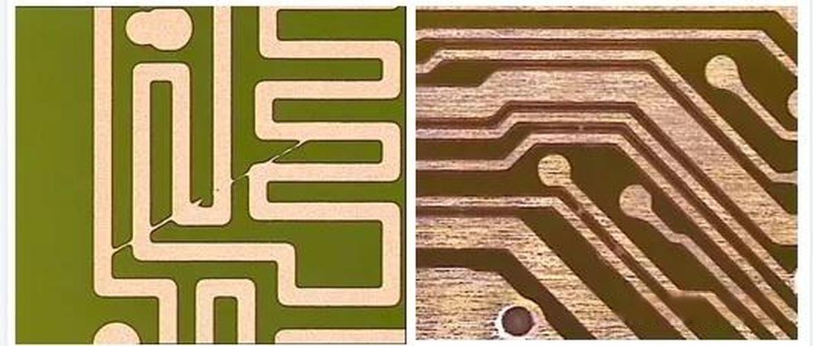
A PCB short circuit is an unintended conductive path between nets that should stay isolated — and in a multilayer board it can hide in places no visual inspection will ever reach: between inner-layer traces, along a rough hole wall, or inside the resin between vias spaced too closely. Shorts found at final test cost a rework cycle; the same short found after the product ships costs a failure analysis.
This guide walks through where short circuits actually originate in multilayer fabrication — design spacing, etch and drill defects, resin systems and CAF growth — and then maps each cause to the detection method that catches it. The goal is practical: by the end, you should be able to read a short-circuit failure on your own board and know which process step to interrogate first.
Table of Contents
- How a PCB Short Circuit Forms Inside a Multilayer Stack
- Design-Side Causes: Spacing, Pads and Plane Clearance
- Fabrication Causes: Etch, Drill and Lamination
- Material-Driven Shorts: Resin Flow and CAF
- Assembly and Mechanical Causes
- How Shorts Are Detected: The Test Chain
- Design Rules That Remove Short-Circuit Risk
- A PCB Short Circuit Found Late: The Failure-Analysis Path
- FAQ
- Want Your Spacing Margins Checked Before Fabrication?
How a PCB Short Circuit Forms Inside a Multilayer Stack
Every PCB short circuit comes down to two conductors getting close enough to touch, or to be bridged by something conductive. In a multilayer stack that can happen in four physically different places, and the place matters because it determines both the detection method and the fix:
- On the surface — trace-to-trace bridging from etch undercuts, solder bridging, or solder-mask coverage gaps. Visually detectable, usually caught by AOI or assembly inspection.
- Between inner layers — copper features from adjacent layers connected through a drill defect or misregistration. Invisible from outside; only electrical test or cross-section finds it.
- Through the hole wall — a drilled hole whose wall breaches into a neighboring conductor, most commonly when hole-to-trace clearance is marginal and drilling wanders.
- Inside the resin — conductive growth between vias over time, the CAF mechanism, which passes electrical test at delivery and fails months later in the field.
A PCB short circuit in the first three places is a manufacturing-time defect; the fourth is a reliability-time defect. Their root causes overlap heavily — spacing and process control dominate all four — but the detection strategies differ, which is why a fabricator’s test regime should be judged against all of them, not just the flying-probe pass rate. The standards that define bare-board acceptance are indexed by the Global Electronics Association standards library.
Design-Side Causes: Spacing, Pads and Plane Clearance
The single biggest driver of short-circuit risk is designed-in: how much copper-to-copper clearance the layout leaves for the fabricator to work with. Etch processes hold spacing to a tolerance — a 3/3 mil design consumes that tolerance differently than a 6/6 mil design, and the margin that remains is what absorbs registration drift, etch undercut and mask misalignment. When the layout runs at the fabricator’s process floor, every downstream wobble converts directly into yield loss or an escaped short.
The classic design-side contributors, roughly in order of how often they show up in failure analysis:
| Design issue | Failure it produces | Prevention at layout time |
|---|---|---|
| Trace-to-trace spacing at the process minimum | Etch bridging on outer layers; margin gone for registration drift | Use ≥ 4 mil spacing unless density forces less; confirm the fabricator’s proven capability first |
| Via-to-trace or via-to-via clearance too tight | Hole-wall breakout touches adjacent conductor | Keep hole-to-copper spacing above the fabricator’s hole-registration tolerance |
| Plane anti-pad too small around via | Via barrel nearly touches plane copper; marginal isolation | Size anti-pads with registration tolerance included, not just electrical clearance |
| Solder mask openings wider than copper | Exposed copper slivers between pads; assembly solder bridging | Match mask opening to pad; specify mask-defined pads where spacing is critical |
| Copper fills and hatched pours without clearance rules | Slivers of unetched copper detach and migrate | Define minimum copper sliver width; avoid isolated copper islands |
None of these rules is exotic — they are exactly the checks a DFM review runs before fabrication starts. The cheapest fix for a PCB short circuit in the industry is a design-rule-check pass that respects the fabricator’s proven spacing capability rather than the theoretical process limit.
Fabrication Causes: Etch, Drill and Lamination
Three fabrication steps generate most manufacturing-time shorts, and each has a characteristic signature:
- Etch. Undercut leaves trapezoidal traces with rough edges; over-plating or resist scum leaves copper slivers between features. A short from etch shows in cross-section as copper bridging at the trace base with clean resist edges above.
- Drill. Wandering or breakout puts a hole wall through neighboring copper. The signature is a crescent-shaped copper intrusion into the hole wall, or a barrel that lands partially outside its pad — which is also where barrel cracking risks cluster.
- Lamination. Layer-to-layer misregistration shifts inner features relative to each other; resin-starved areas leave voids where copper layers can approach. The signature is two nets from different layers connected with no drill involvement — a defect only found by electrical test.
What separates a controlled fabricator from an uncontrolled one is not whether these defects ever occur — they occur everywhere — but whether the process catches them before shipment. That comes down to the inspection chain: inner-layer AOI before lamination catches etch defects when they are still cheap to scrap; post-drill x-ray or coupon checks catch registration drift; final electrical test is the last gate. Skipping any layer of that chain shows up later as an escaped short. The full process sequence and its inspection points are laid out in our PCB manufacturing process guide.
Material-Driven Shorts: Resin Flow and CAF
Two material mechanisms deserve their own section because they fail electrical test in ways that look like process errors:
Resin flow and fill. Prepreg that flows poorly during lamination leaves voids between inner layers — and voids do two bad things at once. They reduce the dielectric spacing between copper features, and they create paths where later moisture ingress lowers surface insulation resistance. A short that cross-sections as copper-to-copper contact through a void line points here, and the fix lives in prepreg selection and press schedules rather than in etch parameters. Our prepreg glass style guide covers how resin content and glass style drive exactly this behavior.
Conductive anodic filament (CAF). CAF is the slow one: copper ions migrate along the glass-resin interface between two vias under bias and humidity, growing a conductive path over months. Boards pass bare-board test and fail in the field. The risk factors are well characterized — via-to-via spacing below roughly 15–20 mils in high-humidity applications, glass styles with bundle-to-resin channels, and bias plus moisture acting together. The countermeasures are also well characterized: wider via spacing, resin systems with better glass wetting, and for harsh environments, filled vias that eliminate the glass interface path entirely.
The practical takeaway: a short found at incoming test and a short found after six months in a humid enclosure are different defect families with different fixes. Diagnosing the second one as a fabrication error wastes everyone’s time — it is a design-and-material decision that was made at quotation. Laminate selection mechanics, including how resin systems differ in this respect, are covered in our laminate selection guide.
Assembly and Mechanical Causes
Some boards arrive perfect and get shorted on the way into the product. The assembly-side mechanisms are familiar from any rework bench:
- Solder bridging between fine-pitch pins — a paste-volume and stencil-aperture issue first, a board design issue second (pad geometry and mask-defined versus non-mask-defined pads change how forgiving the site is).
- Solder mask damage from probing, fixtures or handling, exposing copper that then bridges under contamination.
- Board flex during screwing or connector insertion — a cracked via or a fractured trace can collapse into a short. The mechanical side of this stress story is covered in our warpage and handling guide.
- Conductive contamination — flux residue, metal filings from depaneling, or fibers bridging exposed conductors under bias.
These are caught by assembly-process controls, not by the fabricator — which is why a failure-analysis conclusion that says “assembly-induced short” should be verified with the evidence, not assumed. The cross-section tells the story: solder-metal bridging looks completely different from copper bridging, and the distinction assigns responsibility cleanly.
How Shorts Are Detected: The Test Chain
A fabricator’s defense-in-depth against an escaped PCB short circuit is a chain of checks, each catching what the previous one cannot see:
| Checkpoint | Method | What it catches | Blind to |
|---|---|---|---|
| Inner layers, pre-lam | AOI on each inner-layer panel | Etch bridging, slivers, opens on the layer being imaged | Anything that happens in later layers |
| Post-drill / pre-plating | X-ray registration checks, drill coupons | Hole breakout into copper, layer misregistration | Fine etch defects |
| Pre-shipment, bare board | Electrical test: fixture or flying probe, per netlist | Every electrically detectable short and open, surface and internal | Near-short marginal spacing; future CAF growth |
| Cross-section (coupon) | Microsection per IPC-A-600 | Hole-wall intrusion, layer spacing, voids at interfaces | Random sampling only — not every via |
| Class 3 add-ons | Timed-domain reflectometry on specified nets, impedance coupons | Near-shorts and spacing marginalities that pass pure continuity | Still sampling-based |
Flying probe deserves a note: it needs no fixture, so it adapts to prototypes and low volumes at high accuracy, while universal fixtures test faster once volumes justify the tooling. Either way, the electrical test is only as good as the netlist it tests against — which is why the Gerber-to-netlist extraction step belongs in the quality conversation too. Class requirements tighten all of these gates; the differences are summarized in our IPC Class 2 vs Class 3 guide.
Design Rules That Remove Short-Circuit Risk
The layout rules that most reliably keep shorts out of multilayer builds, in priority order:
- Give spacing headroom. Run ≥ 4 mil copper-to-copper wherever density allows; reserve process-minimum spacing for the nets that genuinely need it.
- Respect hole-to-copper spacing. The drill has a registration tolerance; designs that assume perfect drilling convert that tolerance directly into breakout risk.
- Size plane anti-pads with registration included. An anti-pad that is electrically correct but registration-marginal is a short waiting for one bad panel.
- Prefer mask-defined or matched-mask openings where spacing is critical, so the mask itself becomes part of the isolation strategy.
- Eliminate isolated copper islands and sub-minimum slivers — they etch unpredictably and become conductive debris.
- For humid or high-bias applications, widen via-to-via spacing beyond CAF thresholds, or fill vias to remove the glass-interface path.
Stackup interacts with several of these: dielectric thickness between layers sets how much registration drift the design tolerates, and resin-rich systems handle CAF better. The layer-order logic that underpins these decisions is in our stackup design guide.
A PCB Short Circuit Found Late: The Failure-Analysis Path
When a short shows up after assembly or in the field, the analysis order matters because each step narrows the suspect list:
- Localize electrically — ohmmeter mapping or thermal imaging under bias finds the approximate site faster than visual hunting.
- Image non-destructively — x-ray shows internal copper positions and solder metal; it distinguishes an internal short from a solder bridge immediately.
- Section the site — the cross-section answers the responsibility question: copper-to-copper (fabrication), solder-to-solder (assembly), or conductive growth through resin (CAF, design-and-material).
- Correlate with process records — panel history, drill lot, lamination press data — before assigning the fix.
This is the same disciplined loop used across the defect families in our PCB defects causes-and-fixes guide; the value of the sequence is that it prevents the most expensive mistake in failure analysis — fixing the wrong process step. For long-term mechanisms, the reliability-testing suite that surfaces CAF-prone designs is described in our reliability testing guide.
Frequently Asked Questions
What is the most common cause of a PCB short circuit?
Insufficient copper-to-copper clearance combined with process tolerance drift is the dominant family — spacing at the process minimum leaves no margin for etch undercut, drill wander or layer misregistration. Design-rule violations and fabrication defects each contribute, but most escaped shorts trace back to clearance decisions made at layout time.
Can electrical test miss a short that will fail later?
Yes, in two ways. Marginal spacing that passes continuity can bridge under subsequent thermal or mechanical stress. And CAF growth develops over months under bias and humidity, so a board that passes bare-board test can still fail in the field. Wider via spacing and resin-system choice are the preventions.
How do I tell whether a short was caused by fabrication or assembly?
Cross-section the site. Copper-to-copper bridging with clean laminate edges points to fabrication (etch or drill); solder-metal bridging points to assembly; a conductive path through resin between vias indicates CAF, which is a design-and-material outcome rather than a process error.
What is CAF and why does it matter for multilayer boards?
Conductive anodic filament is a copper migration mechanism that grows along the glass-resin interface between vias under bias and humidity. It develops over months, so boards pass delivery test and fail later. Prevention is via-to-via spacing above the CAF-risk threshold, resin systems that wet glass bundles well, and filled vias in high-risk designs.
Is flying probe testing enough for multilayer prototypes?
Flying probe is the right accuracy-per-cost choice for prototypes and low volumes because it needs no fixture and tests against the extracted netlist. Its limits are the same as any electrical test: it verifies the nets as designed at delivery time, not future CAF growth, and it does not replace cross-section sampling of hole walls and layer spacing.
Why do inner-layer defects matter if they get covered up?
Because a short between inner layers is invisible to visual inspection forever — it can only be caught electrically or by cross-section. That is why inner-layer AOI before lamination is the most valuable inspection checkpoint in the whole chain: it catches defects while the defective panel is still cheap to scrap.
How much copper spacing is safe for a multilayer design?
Use the fabricator’s proven capability, not the theoretical floor. A common comfortable zone is 4–6 mil copper-to-copper for standard multilayer builds; going to 3/3 mil is manufacturable but consumes the tolerance that would otherwise absorb registration and etch drift. Confirm current capability with the fabricator per design.
Can solder mask prevent shorts on fine-pitch components?
Partially. Mask between pads blocks solder bridging during assembly, and mask-defined pad geometries are more forgiving on tight spacing. But mask does not protect inner layers or through-hole walls, so it complements — never replaces — electrical test and spacing-driven design rules.
Want Your Spacing Margins Checked Before Fabrication?
Send your Gerber package and we will run the spacing, hole-to-copper and anti-pad checks against proven process capability, flag the marginal clearances, and confirm the electrical-test coverage before quotation. Production runs from 2 to 30 layers (up to 64 layers for prototypes, subject to per-order review), with process feedback typically the same day.
Season PCB direct: Tel (+86) 18681528532 | WhatsApp +86 18681528532
E-mail: roc@season-pcb.com