Book Appointment Now

PCB pad lifting explained: five root causes, peel-strength and thermal-stress tests, rework rules, and design choices that keep pads attached.
PCB Pad Lifting: Causes, Tests and Prevention Rules
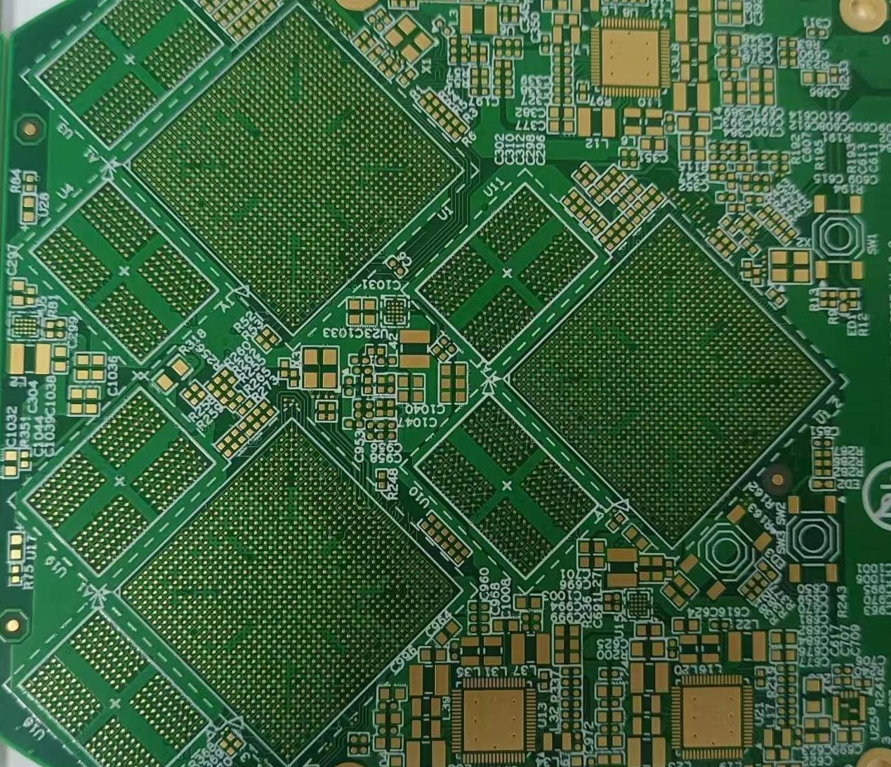
A lifted pad usually shows up at the worst possible moment: during rework, when a technician lifts a component lead and the copper pad comes up with it, leaving bare laminate behind. Pad lifting is the separation of a copper pad or trace from the underlying laminate. It almost always traces back to a combination of material choice, fabrication process control and mechanical handling — not to a single dramatic mistake.
This guide separates the two failure modes that get lumped together (interfacial pad lifting versus resin fracture known as pad cratering). It walks through the five root causes, the tests that expose weak adhesion before assemblies are built. It then covers the design and rework rules that prevent the failure in the first place. It is written from the buyer’s side of the table: what to specify, what to ask for, and what a first-article review should check.
Table of Contents
- What Pad Lifting Actually Is — and How It Differs from Pad Cratering
- The Five Root Causes of Lifted Pads
- The Interface Failure Zone: Where Copper Meets Resin
- Tests That Catch Weak Pads Before Assembly
- Design Rules That Keep Pads Attached
- Rework: Where Most Pad Lifting Damage Is Made
- What to Ask a Fabricator About Pad Adhesion
- Acceptance Criteria and the First-Article Review
- Prevention Checklist: Before You Send the Next Order
- FAQ
- Have a Pad-Related Failure or a Design Worth Stress-Reviewing?
What Pad Lifting Actually Is — and How It Differs from Pad Cratering
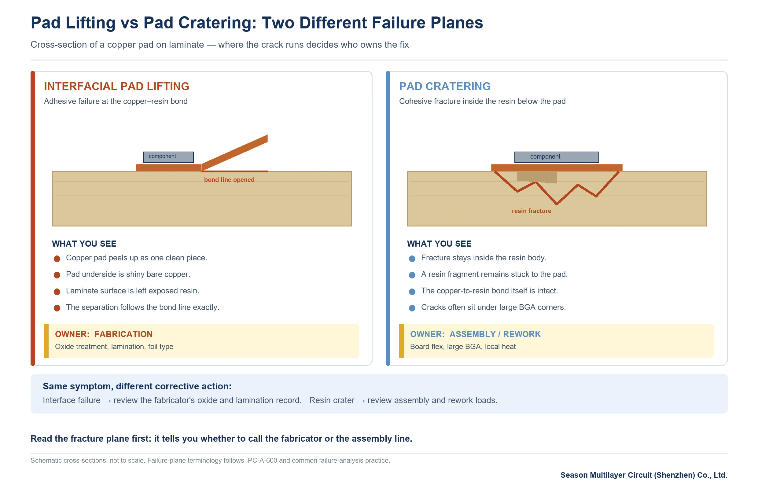
The term covers two mechanically different failures, and telling them apart changes the entire corrective-action path:
- Pad lifting (interfacial failure) — the copper-to-laminate bond fails. The pad peels cleanly away, and the underside looks shiny copper while the laminate surface shows exposed resin or the treatment layer. This is a fabrication-side adhesion problem in most cases.
- Pad cratering (bulk fracture) — the copper bond holds, but the resin underneath fractures. A crater of laminate material stays stuck to the pad. This is typically a mechanical or thermal-mechanical overstress event during assembly, rework or handling, and it is the dominant mode under large BGA packages.
The distinction matters because interfacial lifting points to the fabricator’s oxide treatment, lamination schedule or copper-foil selection, while cratering points to assembly stresses, board stiffness and support during rework. Misdiagnosing one as the other sends both engineering teams chasing the wrong variable.
The Five Root Causes of Lifted Pads
Field failures almost always fall into one of five buckets. The first decision table summarizes them with the confirming evidence for each:
| Symptom observed | Most likely root cause | Confirming evidence | Primary fix |
|---|---|---|---|
| Pad lifts during first reflow or rework, underside shiny copper | Weak copper-to-resin adhesion (oxide treatment or lamination defect) | Peel strength below the table’s minimum on cross-section coupons | Fabricator process audit: brown-oxide line, lamination parameters |
| Pad lifts with a matte, dull underside and resin stuck to it | Bulk resin fracture (pad cratering) from mechanical overstress | Fracture plane runs through resin, not the interface | Assembly-side: support fixtures, screw torque, connector handling |
| Lifting concentrated near large copper pours or heavy components | Coefficient-of-thermal-expansion (CTE) mismatch stress in the z-axis | Failures cluster after thermal cycling; warpage history present | Balanced stackup, higher-Tg or lower-CTE laminate, stress relief |
| Lifting after multiple rework cycles at the same site | Cumulative thermal damage to the resin at the interface | Discoloration of laminate around the pad; history of repeated touch-up | Cap rework cycles, lower tip temperature, preheat before desoldering |
| Lifting on freshly delivered bare boards before any soldering | Moisture absorption or handling damage between fab and assembly | Blisters on other pads; boards stored unsealed in humid shipping | Vacuum-sealed packaging with desiccant, bake-out before reflow |
Two of these five are entirely within the fabricator’s control (interface adhesion and stackup balance), one is shared (moisture management), and two belong to assembly and handling. A pad-lifting complaint that names all five suspects at once is usually a conversation that has not yet looked at the fracture surface.
The Interface Failure Zone: Where Copper Meets Resin
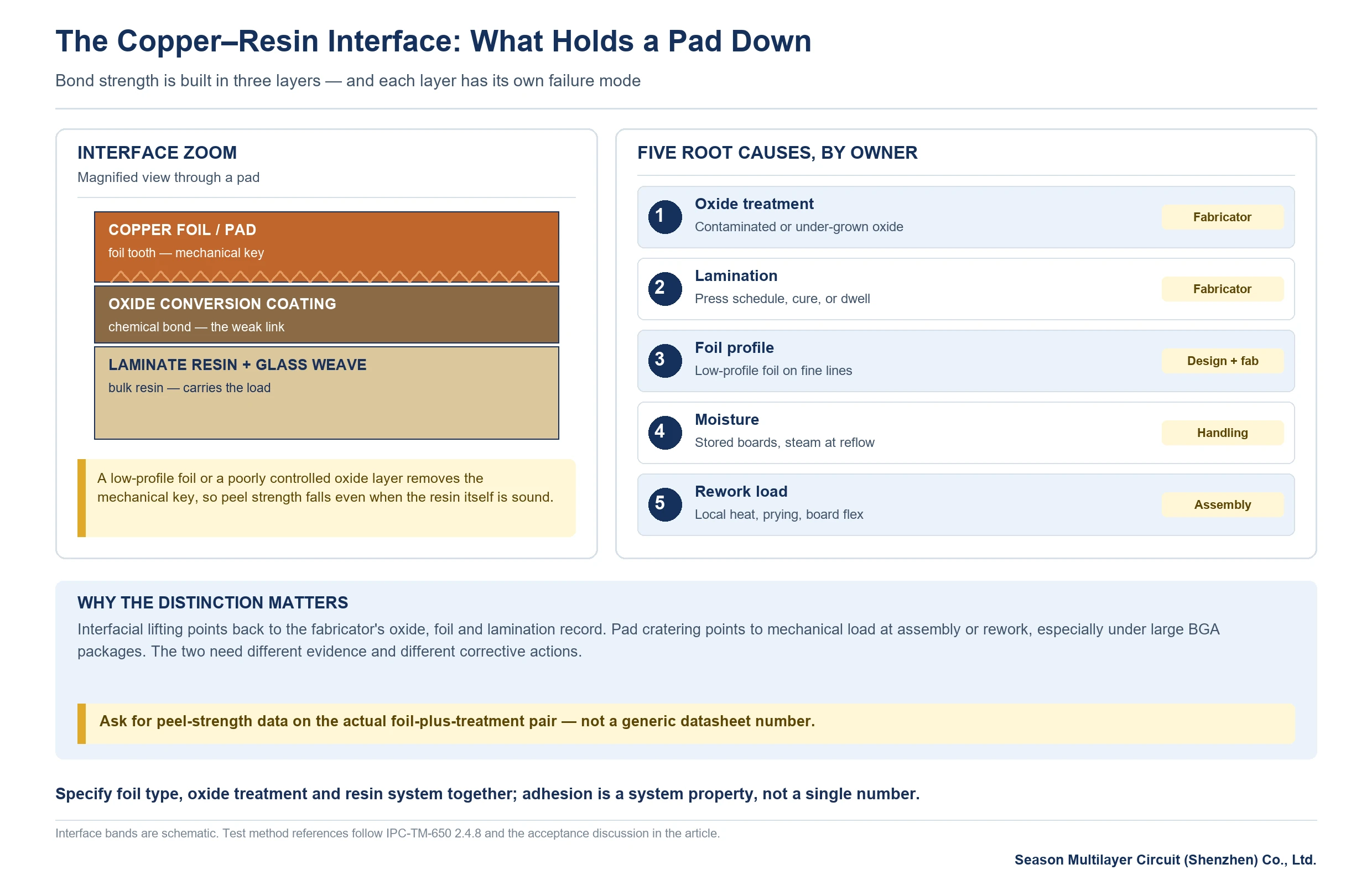
Copper does not bond mechanically to epoxy resin — it bonds chemically through an oxide treatment applied before lamination. The inner-layer brown-oxide (or black-oxide) process grows a needle-like crystalline layer on the copper surface that resin flows into during pressing, creating a mechanical-chemical interlock. If that layer is too thin, unevenly grown, or contaminated by fingerprint oils and resist residues, the interlock never forms and the pad sits on a weak interface from day one.
Foil type is the other half of the story. Standard electrodeposited foil has a relatively smooth drum side; the tooth profile that anchors into resin lives on the matte side. Low-profile and very-low-profile foils (RTF, HVLP) trade some of that mechanical tooth for better etch definition on fine-pitch designs, which is why fabricators compensate with tighter oxide-process control. The practical takeaway for a buyer: when a design specifies low-profile foil for fine lines, ask what oxide treatment goes with it, and ask for peel-strength data on the actual foil-plus-treatment combination rather than a datasheet number for generic foil.
Resin system completes the triangle. High-Tg and low-CTE laminates hold the interface together better through reflow cycles because they physically move less in the z-axis; moisture-resistant resins keep the bond from hydrolyzing during storage. This is why the same design can show pad lifting with one laminate and survive happily with another — and why a root-cause analysis that stops at “the soldering was too hot” often misses the material variable. Our laminate quality guide covers how resin selection and storage conditions interact.
Tests That Catch Weak Pads Before Assembly
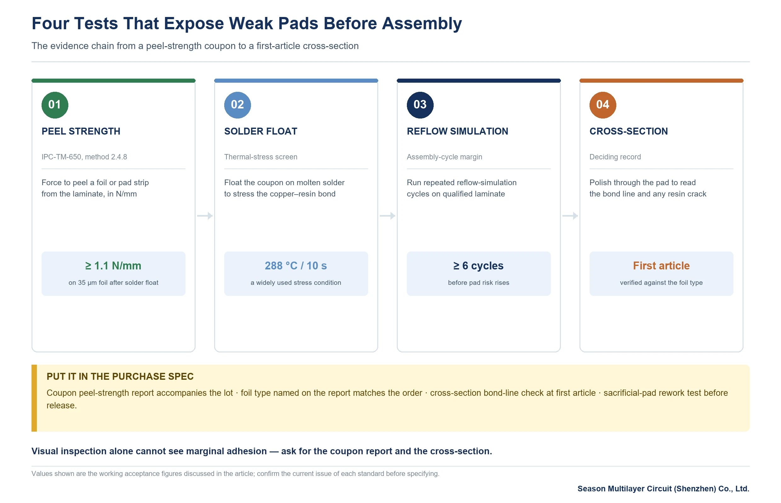
Every mechanism above has a bench test that exposes it, and all of them run on coupons or production panels before any component is placed:
| Test | What it measures | Typical acceptance for Class 2 builds |
|---|---|---|
| Copper peel strength (IPC-TM-650, method 2.4.8) | Force to peel foil or a pad strip from laminate, in N/mm | ≥ 1.1 N/mm on 35 µm foil after solder-float conditioning |
| Solder-float / thermal stress (288 °C, 10 s) | Interface survival through soldering-level thermal shock | No blistering or delamination; repeated per class requirement |
| 6× reflow simulation | Cumulative z-axis CTE stress through multiple thermal cycles | No interconnect or interface degradation on microsection |
| Cross-section of plated pads | Bond integrity, oxide-layer coverage, resin wetting at the interface | Continuous bond line; no separation at copper-to-resin boundary |
| IST or thermal-cycling coupons | Field-style survival of the interface over repeated power cycles | Resistance change within plan limits across defined cycles |
The copper peel strength row is the one worth insisting on in writing. It is cheap, fast, and it directly measures the interface that fails in the field — and it must be run on the actual foil-and-treatment combination, because a datasheet minimum for a different foil type says nothing about your build. Acceptance-class rules interact here too: Class 3 imposes tighter requirements across the board, and the differences are summarized in our IPC Class 2 vs Class 3 comparison. The broader standards landscape is indexed by the Global Electronics Association standards library.
Design Rules That Keep Pads Attached
Design decisions move the failure threshold as much as process control does. Four of them matter most in practice:
- Teardrop pad-to-trace transitions. A fillet where a trace meets a pad spreads peel stress over a wider copper area. Sharp right-angle junctions concentrate stress at the thinnest copper point and are a classic initiator for trace lifting that starts at the pad edge.
- Thermal relief on plane-connected pads. Pads tied solidly into large copper pours solder poorly and stress unevenly during reflow because the pour acts as a heat sink. Spoked thermal-relief connections balance solderability against electrical performance.
- Anchored, not floating, repair pads. Where a pad connects only to a via or a short stub, it has almost no peel resistance. Connecting pads on both sides — even with a thin trace — multiplies the force needed to lift them.
- Via-in-pad with fill. An unfilled via under a component pad is a void and a stress riser at once. Filled and capped vias turn the pad into a solid structure; the process trade-offs are covered in our via-in-pad technology guide.
None of these rules costs money at quotation — they cost a design-review pass. That is exactly why folding them into a DFM review checklist before fabrication is cheaper than discovering them on a cross-section after a field return. For designs where the pad-lifting risk concentrates under a large package, pairing these rules with a properly balanced layer stack is the remaining lever; the stackup logic is laid out in our PCB stackup design guide.
Rework: Where Most Pad Lifting Damage Is Made
Statistics from failure-analysis labs keep repeating the same pattern: a large share of lifted pads in returned assemblies were manufactured with perfectly adequate adhesion, then damaged during rework. A soldering iron run above 370 °C, a desoldering pump applied before the joint is fully liquid, or a lead pulled sideways while the solder is still plastic — any of these applies peel loads the pad was never designed to take.
Three rework rules keep the pad on the board:
- Preheat the board from the underside to within roughly 100 °C of the working temperature before any contact, so the joint reaches liquidus without the iron carrying the entire thermal load.
- Cap contact cycles — as a working practice, no more than two reflow cycles at the same joint, because resin at the interface degrades cumulatively even when each cycle looks clean.
- Pull leads axially, never sideways, and support the board flat underneath the work area so flex does not turn into a peel load on the pad.
Boards that travel between contract manufacturers add another failure vector: unsealed storage in transit lets laminate absorb moisture, and the steam expansion during reflow — the popcorn effect — attacks the interface from inside. Vacuum-packed shipments with desiccant, plus a bake-out before reflow when storage history is uncertain, close that gap cheaply.
What to Ask a Fabricator About Pad Adhesion
Pad adhesion is not a glamorous capability, which makes it a good probe of overall process discipline. A short question list gets past the marketing layer quickly:
- Which oxide treatment runs on inner layers, and is the line chemistry monitored and logged per shift?
- What foil types are stocked (standard, RTF, HVLP), and is copper peel strength verified on the foil-treatment combination actually used for the order?
- Are lamination press schedules recorded and traceable to the panel, including heat-up rate and peak dwell?
- Is solder-float or reflow-simulation testing standard on cross-section coupons, and are the coupons retained?
- What is the standard packaging for finished boards — vacuum seal with desiccant, or loose in a plastic bag?
The answers to the last two questions predict pad-lifting complaints better than most audit checklists, because they reveal whether the fabricator treats the interface as a controlled feature or as something that comes along for free. For context on how adhesion fits into the wider defect landscape, our PCB defects guide maps the failure families, and the plated-hole counterpart — barrel cracking — is analyzed separately in our barrel crack guide.
Acceptance Criteria and the First-Article Review
IPC-A-600 gives the visual acceptance framework for bare boards: pad lifting, in any degree, is not an acceptable condition on a delivered board, and blisters that bridge conductors or lift pads are treated as rejects. The inspection burden, however, is on the sample — which makes the first-article review the natural checkpoint for everything in this guide:
- Cross-section two or three pads of each type, including the smallest and the largest, and check the bond line continuity at the copper-resin interface.
- Confirm the coupon peel-strength report accompanies the lot, with the foil type named on the report matching the order.
- Wick one sacrificial pad with a soldering iron at production rework settings and confirm it survives — an intentionally crude but honest test of what assembly will actually do to the board.
- Check packaging on arrival: sealed bag, desiccant present, humidity indicator card if specified.
Surface finish interacts with all of this more than buyers expect: a finish applied over a weak interface hides it until the first reflow, while finishes like ENIG bring their own pad-related failure modes that deserve separate attention — the nickel-layer problems are covered in our ENIG solderability guide, and the finish-selection trade-offs in our surface finish comparison.
Prevention Checklist: Before You Send the Next Order
Condensed to a single page, the working prevention checklist reads:
| Stage | Action | Owner |
|---|---|---|
| Design | Teardrops on pad-trace junctions; thermal relief on plane-connected pads; no floating stub pads | Design / CAD |
| Material | Resin system with Tg and CTE matched to the reflow profile; moisture-resistant laminate for humid supply chains | Design + fabricator |
| Fabrication | Oxide process control; copper peel strength on the actual foil-treatment pair; recorded press schedules | Fabricator |
| Incoming | Sealed packaging with desiccant; bake-out if storage history is uncertain | Assembly |
| Assembly | Preheat before rework; axial lead removal; board support under the work area; capped rework cycles | Assembly |
| First article | Cross-section bond-line check; coupon peel report verified against foil type; sacrificial-pad rework test | Quality |
Nothing on the list is exotic, and that is the point: pad lifting is almost never caused by a single advanced-process failure. It accumulates from ordinary decisions made slightly carelessly — an oxide bath drifting out of range, a rework station without preheat, a shipment in an unsealed bag. The failure analysis loop is closed in our warpage causes and rework guide, which covers the mechanical side of the same stress story.
Frequently Asked Questions
What is the difference between pad lifting and pad cratering?
Pad lifting is an interfacial failure: the copper pad separates cleanly from the laminate and the underside shows bare copper. Pad cratering is a bulk resin fracture: the copper bond holds and a crater of laminate material stays attached to the pad. Lifting usually points to fabrication-side adhesion, cratering to assembly-side mechanical overstress.
Can a lifted pad be repaired?
Small pad lifts can sometimes be repaired by scraping back to sound copper, adding a jumper wire anchored to a surviving feature, and potting the area. But the repair is only as strong as the remaining anchor. On fine-pitch or BGA sites the practical repair is a jumper to the nearest via. Repeated repairs at one site should trigger a root-cause review instead of another patch.
What peel strength should I specify for a multilayer board?
A common working floor is 1.1 N/mm for 35 µm (1 oz) foil measured after solder-float conditioning, per IPC-TM-650 method 2.4.8. The more important detail is that the value be measured on the actual foil-and-oxide combination used for your order, not a generic datasheet figure.
Why do pads lift more often during rework than during the first assembly?
First assembly runs a controlled reflow profile. Rework concentrates heat through a single iron or nozzle, often without board preheat, and applies mechanical force to leads. Each rework cycle also cumulatively degrades the resin at the interface, so the same pad that survived the first reflow can fail on the second touch-up.
Does moisture really cause pad lifting?
Yes, indirectly. Absorbed moisture expands to steam during reflow — the popcorn effect — and that internal pressure attacks the copper-to-resin interface and can produce blistering across pads. Vacuum-sealed packaging with desiccant, and a bake-out before reflow when storage history is unknown, removes the risk at negligible cost.
Which design features make pads more resistant to lifting?
Teardrop transitions where traces meet pads, thermal-relief spokes on plane-connected pads, connections on both sides of the pad rather than a single stub, and filled vias under component pads. All of them spread or remove peel stress from the thinnest copper region.
Are lifted pads visible before assembly?
Sometimes. Severe blistering or lifting is visible under magnification on incoming inspection, but marginal adhesion looks perfectly normal on the surface. That is why peel-strength coupons and cross-sections, not visual inspection, are the reliable early detectors.
How many reflow cycles can a PCB survive before pad risk rises?
A well-made laminate system is qualified for at least six reflow-simulation cycles in standard test flows. In production practice, keep rework at any single joint to two cycles or fewer, and treat a third touch-up as a signal to review the root cause instead of repeating the same repair.
Have a Pad-Related Failure or a Design Worth Stress-Reviewing?
Send your stackup, surface finish and the pad geometry you are most concerned about, and our engineering team will review the adhesion-relevant variables — foil type, oxide treatment and reflow thermal load — before quotation. Production runs from 2 to 30 layers (up to 64 layers for prototypes, subject to per-order review), and process feedback typically comes back the same day. You can also request an instant PCB quote with the pad geometry attached. Related starting points: our PCB manufacturing process overview.
Season PCB direct: Tel (+86) 18681528532 | WhatsApp +86 18681528532
E-mail: roc@season-pcb.com