Book Appointment Now

How a 6-layer 2-stage HDI headphone PCB is built: the 2+2+2 stackup, microvia chains, 0.25 mm BGA fan-out, thin-board stiffness and prototype lead times.
Headphone PCB: 6-Layer 2-Stage HDI for TWS and Audio Design
A true wireless headphone PCB has to fit a Bluetooth SoC, power management, battery charging, an antenna field and two microphones into a board smaller than a fingernail — and do it at 0.8 mm thick. That combination of density and thinness is exactly what a 6-layer 2-stage HDI build exists for, and it is the structure behind most serious TWS earbud designs today.
This guide walks through a real production build step by step: the 2+2+2 stackup and its two-stage microvia chains, the design rules that make 0.25 mm BGA fan-out work, the mechanical constraints of a thin board, and the cost and sourcing picture. If you are comparing HDI stages for the first time, the HDI PCB technology guide explains how 1-stage, 2-stage and any-layer builds differ across the full product range.
Table of Contents
- Why a TWS Headphone PCB Needs 2-Stage HDI
- Reference Build: Specifications at a Glance
- Inside the 2+2+2 Stackup
- Two-Stage Microvia Chains: Staggered vs Stacked
- Routing Density: 0.25 mm BGA Fan-Out on a Headphone PCB
- Designing a 0.8 mm Thin Board Without Warpage
- Audio and RF Signal Integrity on a Headphone PCB
- 2-Stage HDI vs Conventional Through-Hole
- Cost Drivers and How to Source a Headphone PCB
- FAQ
- Get Your Headphone PCB Stackup Reviewed
Why a TWS Headphone PCB Needs 2-Stage HDI
The defining constraint of a TWS earbud is volume. Everything the product does — radio, audio codec, power, sensing — shares a few square centimeters, and the battery takes most of that. The SoC lands in a 0.25 mm pitch BGA, and the passive count around it keeps growing with each feature generation. A conventional through-hole or even a 1-stage HDI build runs out of escape routing before the schematic is fully connected.
Two buildup stages change the math. With laser microvias spanning two dielectrics per side, every BGA ball can reach an inner routing layer, traces drop between layers inside the escape field instead of snaking across it, and the antenna keep-out area stays clean. The extra stage costs more than a 1-stage build, but on a density-limited product it is usually the difference between a routable layout and an impossible one.
There is a second, quieter reason: thickness. A 0.8 mm board with two buildup stages puts its two copper cores close together at the center, leaving the outer layers free for fine-pitch escape. The same thickness achieved by shrinking a 4-layer core stack would leave no room for the BGA at all.
Reference Build: Specifications at a Glance
The parameters below come from a production TWS motherboard build. They are a practical quoting baseline: each value sits inside standard process windows, which keeps yield high and lead times short. Values at the edge of a window are possible but belong in an engineering review, not a first quotation.
| Parameter | Reference build |
|---|---|
| Layer count | 6 layers, 2-stage HDI (2+2+2) |
| Base material | Tg 170 FR-4 grade |
| Finished thickness | 0.8 mm |
| Panelization | 130.5 × 85.8 mm panel, 20 boards up |
| Outer copper | 35 µm (1 oz) |
| Inner copper | 18 µm (0.5 oz) |
| Minimum plated through-hole | 0.20 mm |
| Minimum laser blind via | 0.10 mm |
| Minimum BGA pitch | 0.25 mm |
| Trace and space | 3/3 mil |
| Surface finish | ENIG |
The 20-up panel is worth noticing. Small earbud boards only make economic sense when dozens share a panel through every process step, so panelization strategy influences unit price more than almost any other decision on this class of product. The 0.10 mm laser via is the standard capability limit; 0.076 mm is available case by case after engineering review.
Inside the 2+2+2 Stackup
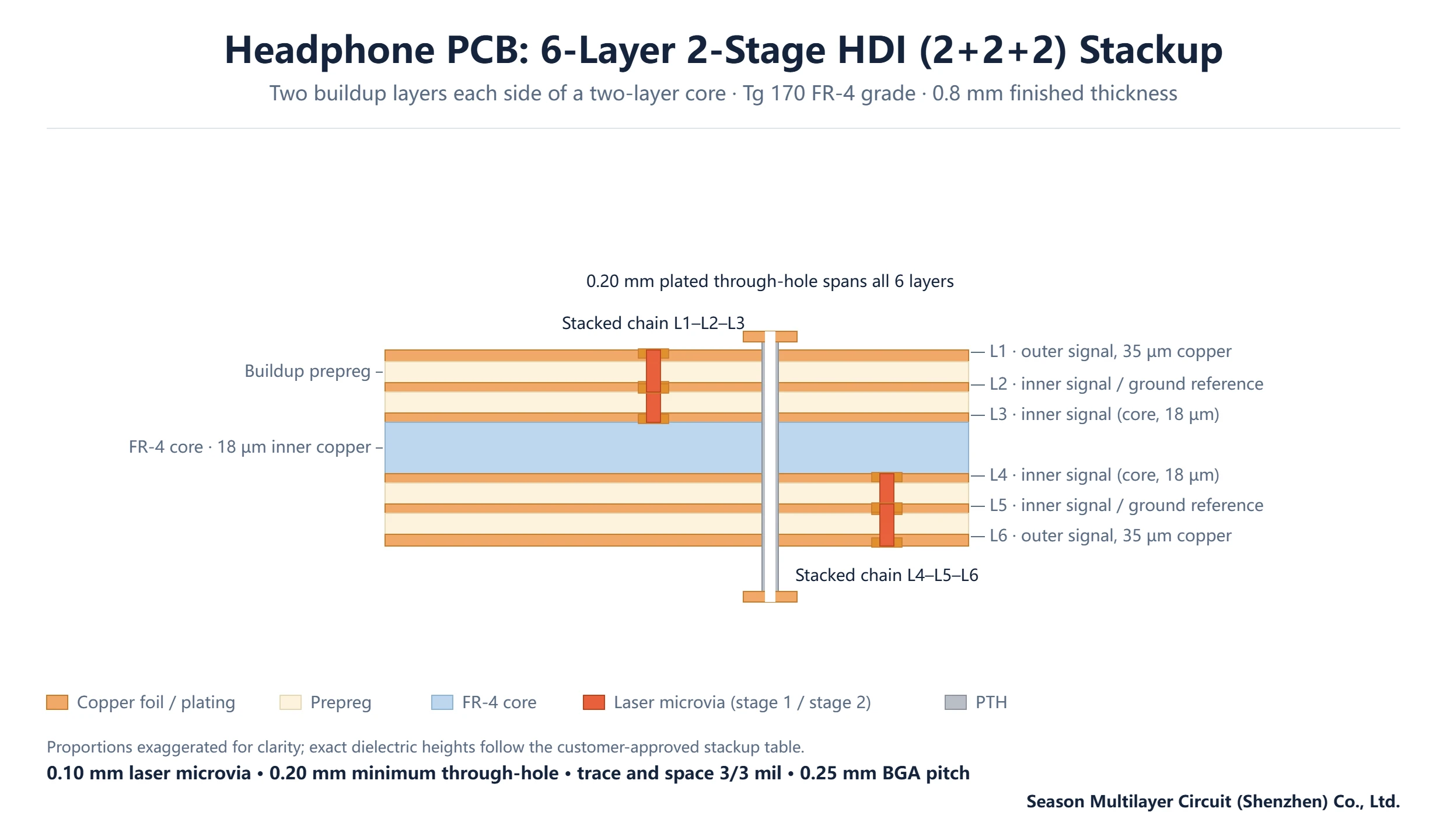
The 2+2+2 notation means two buildup layers on each side of a two-layer core. The core sub-board — a single FR-4 core carrying L3 and L4 — is laminated first. The first buildup pair is pressed on, and stage-1 laser microvias connect L2 to L3 and L5 to L4. The second buildup pair follows, and stage-2 microvias connect L1 to L2 and L6 to L5.
| Layer | Function | Microvia stage |
|---|---|---|
| L1 | Outer signal, component pads and antenna feed | Stage-2 via down to L2 |
| L2 | Inner signal / ground reference | Stage-1 via down to L3 |
| L3 | Inner signal (core, 18 µm) | Landing layer for stage-1 via |
| L4 | Inner signal (core, 18 µm) | Landing layer for stage-1 via |
| L5 | Inner signal / ground reference | Stage-1 via up to L4 |
| L6 | Outer signal and component pads | Stage-2 via up to L5 |
Each stage is laminated and drilled before the next one starts, so alignment accumulates: the stage-2 via must land on a stage-1 via or pad that was placed one lamination cycle earlier. That registration chain is the main process risk of a 2-stage build, and it is why fabricators hold tighter layer-to-layer registration tolerance here than on any 1-stage product.
Two-Stage Microvia Chains: Staggered vs Stacked
A chain from L1 to L3 can be built two ways. In a staggered chain, the stage-2 via lands beside the stage-1 via on L2 and connects through a short surface trace on that layer. In a stacked chain, both vias share one axis, and the stage-2 via sits directly on top of the stage-1 via. The figure below shows both options.
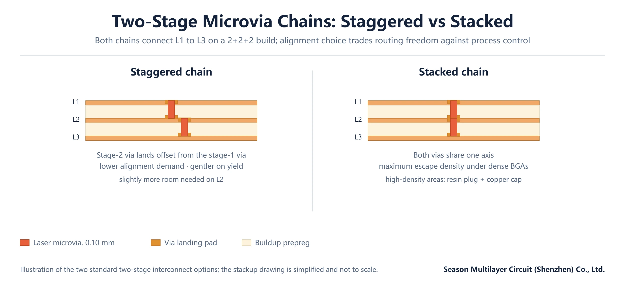
Staggered chains are gentler on yield: the alignment demand between laminations is looser, and each via is a simple drilled-and-plated structure. Stacked chains save the L2 landing footprint, which matters under a dense BGA where every square tenth of a millimeter counts. Where stacked chains are used in the high-density escape field, the vias are filled with resin and capped with plated copper, producing a flat, solid interconnect that survives multiple reflow cycles without voids.
The practical rule: use staggered chains wherever routing allows and reserve stacked, filled structures for the BGA escape field. That split keeps process risk concentrated in the small area where the density actually demands it.
Routing Density: 0.25 mm BGA Fan-Out on a Headphone PCB
At 0.25 mm pitch, the gap between adjacent balls is roughly 0.13 mm after pad diameter is subtracted — not enough for a trace, and not enough for a through-hole in any configuration. The escape strategy therefore leans entirely on microvias: each ball gets a laser via, and routing moves to L2 or L3 where the 3/3 mil window opens up. With two stages, even the center rows of the BGA escape cleanly downward.
Two rules keep this field manufacturable. First, keep the via chain length consistent within a cluster; mixed staggered and stacked chains under the same BGA create uneven plating and registration stress. Second, respect the 0.25 mm minimum BGA pitch as a hard floor in the layout tool — designing to 0.22 mm because one corner of the die allows it will fail at the fabricator’s CAM review and cost a full design cycle.
If the same product family also includes a desk or speaker variant with more board area, check whether 1-stage HDI is sufficient before inheriting the 2-stage stackup; the HDI PCB vs standard PCB comparison quantifies the density and cost crossover between the classes.
Designing a 0.8 mm Thin Board Without Warpage
A 0.8 mm finished thickness leaves little material to resist bending, so copper and dielectric distribution become primary design decisions rather than afterthoughts. The 2+2+2 structure helps by symmetry: identical buildup stacks on both faces, the two cores centered, and balanced copper coverage across all six layers. An asymmetric stackup of this thickness will bow visibly after lamination and refuse to feed through the SMT lines reliably.
The 18 µm inner copper also plays a role. Thin inner layers keep the total stack within the 0.8 mm budget, but they reduce current capacity on inner power paths, so power routing belongs on the outer layers where 35 µm is available, or on wide inner traces with short loops. Panel handling matters too: a 20-up panel of thin boards needs carrier support through the heavier process steps, which the fabricator handles but which slightly influences cost.
Finally, the stiffening structures a housing provides — battery shelf, antenna bracket, connector boss — should be identified early. Boards this thin rely on the assembly for rigidity, and a mounting point that arrives unsupported in the mechanical design becomes a cracked solder joint in the field.
Audio and RF Signal Integrity on a Headphone PCB
A headphone PCB carries two signal families with opposite personalities: the Bluetooth radio at 2.4 GHz, and analog or digital audio at the lowest speeds on the board. The 2-stage stackup serves both by giving each its own reference structure — L2 as a ground plane under the RF section, and clean, wide returns under the audio paths — without burning extra layers that the escape field needs.
Impedance control concentrates on the RF feed and any high-speed digital interfaces between the SoC and memory. Production windows follow the standard tiers: ±10% for single-ended RF lines, ±8% for differential pairs, and ±5% only where a specific interface demands it. Verified impedance on a TWS board is cheap insurance; an uncontrolled antenna feed shows up as unit-to-unit radio range variation that is miserable to debug at the assembly level.
Microphone and speaker lines deserve layout discipline even though they are slow: keep them away from the antenna keep-out and the power switching section, and give them a continuous reference. Most audio complaints traced back to PCB layout turn out to be return-path interruptions, not component choices — a pattern documented across many consumer audio designs.
2-Stage HDI vs Conventional Through-Hole
The comparison below frames when the 2-stage build earns its premium and when it does not. The numbers describe this reference class; individual designs shift the crossover, but the shape of the trade is stable across the industry.
| Aspect | 2-Stage HDI | Conventional through-hole |
|---|---|---|
| Interconnect structure | Laser microvia chains, L1→L2→L3 per side | Mechanical through-holes only |
| Minimum via diameter | 0.10–0.15 mm | 0.20 mm and above |
| 0.25 mm BGA fan-out | Direct escape through the via chain | Generally not routable |
| Best suited for | Miniaturized, high-density audio and wearable boards | Larger, cost-driven designs |
| Relative cost | Roughly 1.3–1.8× | 1.0× |
The cost multiplier is real but concentrated: it buys escape density that no other structure provides at 0.8 mm. Where the BGA pitch relaxes to 0.4 mm or the board area grows, a 1-stage or even through-hole build becomes viable again, which is why the stage decision belongs at the start of the design, not in the quoting email. Acceptance criteria for either structure come from the same source: the IPC qualification and performance standards that govern rigid board fabrication (IPC standards overview).
Cost Drivers and How to Source a Headphone PCB
Four levers dominate the unit price of this build. Panelization comes first: the 20-up panel spreads every fixed process cost across twenty boards, and a naive 6-up panel can double the unit price without changing a single design parameter. Stage count is second — each additional lamination and laser cycle adds cost, as covered above. Trace and space at 3/3 mil keeps outer-layer yield high, and ENIG protects the fine-pitch pads through multiple assembly passes.
Sourcing is straightforward when the data package is complete. Send Gerber data with drill files, the stackup intent, the impedance table and assembly requirements; Season PCB maintains a configured product page for exactly this class — the 6-layer 2-stage HDI headphone PCB — so the review can start from known-good process windows. Prototype builds typically complete in 5–7 working days and production batches in 15–20 working days, both confirmed at engineering review.
Volume scaling for consumer audio runs through the same process as prototype: the group’s three plants hold an annual capacity of 3,000,000 m² across 2–30 layers, and a design validated on the prototype line moves to volume tooling without requalification. Sister builds in the same product family — for example the 6-layer 2-stage HDI sound card PCB — share the stackup, which shortens qualification when the product line expands.
Frequently Asked Questions
What does a 2+2+2 stackup mean on a headphone PCB?
It means two buildup dielectric layers on each outer side of a two-layer FR-4 core. The core is laminated first, then each buildup pair is pressed and laser-drilled in sequence, producing two microvia levels per side — the structure abbreviated as 6-layer 2-stage HDI.
When does a TWS design need 2-stage HDI instead of 1-stage?
When the BGA escape field cannot close with a single microvia level. As a working rule, 0.25 mm pitch BGAs with more than a few hundred balls need the second stage; at 0.4 mm pitch or on larger boards, 1-stage usually routes clean and saves cost. Decide at stackup definition, not at quotation.
How small can laser microvias go on this build?
0.10 mm is the standard production capability for laser blind vias, and this reference build uses it directly. 0.076 mm is achievable case by case after engineering review, since it pushes pad sizes and registration demands toward the limit of the laser drilling and plating process.
Can the microvias in the fan-out area be filled?
Yes. In high-density areas, stacked microvias are filled with resin and capped with plated copper, giving a flat solid via that tolerates multiple reflow passes. Fill quality is verified by cross-section on first articles, with the sections archived batch by batch.
Is a 0.8 mm thick headphone PCB fragile?
It is workable when the stackup is symmetric and the housing provides the mounting support. The 2+2+2 structure balances copper and dielectric about the board center, which controls bow and twist through lamination; fragility problems almost always trace to asymmetric stackups or unsupported mounting points, not to the thickness itself.
What files should I send for a headphone PCB quote?
Gerber data with drill files, the intended stackup, the impedance table with tolerance classes, and assembly requirements including surface finish. A complete package lets the fabricator return a process review and price in one round; missing impedance intent is the most common cause of quote delays.
How long does a 6-layer 2-stage HDI prototype take?
Prototype builds typically complete in 5–7 working days and production batches in 15–20 working days, both confirmed at engineering review after the Gerber check. Stacked via chains in the escape field can add a registration review, so flagging them early keeps the schedule accurate.
Get Your Headphone PCB Stackup Reviewed
Submit your Gerber data and stackup intent for an engineering review before release: the team confirms the microvia chain strategy, BGA escape feasibility and panelization in a single pass. For the wearable sibling of this build class, the 6-layer 1-stage HDI kids smartwatch PCB page shows how the same density problem is solved one stage down, and the any-layer HDI guide covers what comes after 2-stage when a future design shrinks further.
Get Your Headphone PCB Build Reviewed Before You Commit
If the build described above is close to your design, send the stackup intention and Gerber data for engineering review. We return feasibility comments on layer count, via structure and panel efficiency, plus the production detail behind the 6-layer 2-stage HDI headphone PCB in this article. Anything outside standard process windows is flagged with the cost and lead-time deltas attached, before you commit a layout.