Book Appointment Now

A 6-layer 1-stage HDI rearview mirror PCB reference build, covering the 1+4+1 stackup, BGA escape rules, impedance windows and automotive qualification steps.
Rearview Mirror PCB: 6-Layer 1-Stage HDI Stackup and Specs
A modern rearview mirror PCB carries far more than a glass mirror: camera input, a display driver and, on smart-cockpit variants, a full application processor all share one small board. That integration is why the 6-layer 1-stage HDI build in this guide has become the default architecture for automotive mirror modules. If you are sourcing this board class for the first time, the specification numbers below come from a real production build, not a template.
This article breaks the build into the three decisions that actually drive cost and reliability: the 1+4+1 stackup, the impedance and design-rule windows, and the qualification steps a mirror module has to survive. A companion HDI PCB technology guide covers the wider process background if you need it.
Table of Contents
- Why a Rearview Mirror PCB Moved to 6-Layer 1-Stage HDI
- Reference Build: Specifications at a Glance
- Inside the 1+4+1 Stackup
- Impedance Control and Reference Planes
- Design Rules for 0.20 mm BGA Escape
- Automotive Reliability Requirements on a Rearview Mirror PCB
- What Drives the Cost of a 1-Stage HDI Build
- Manufacturing and Quality Control Checks
- Sourcing a Rearview Mirror PCB: Files and Lead Times
- FAQ
- Get Your Rearview Mirror PCB Stackup Reviewed
Why a Rearview Mirror PCB Moved to 6-Layer 1-Stage HDI
Early mirror modules needed only a motor driver and a lamp circuit, which a two-layer board handled without effort. A smart mirror is a different product: it processes a live camera stream, drives a display, and talks to the vehicle network at the same time. The processor that does this work sits in a fine-pitch BGA package, and a conventional through-hole stackup cannot escape 0.20 mm pitch balls within two layers.
A 6-layer 1-stage HDI build solves the escape problem with one layer of laser blind microvias on each outer surface while keeping the lamination flow close to a standard multilayer process. That is the practical compromise: enough routing density for the BGA, without the cost and cycle count of a 2-stage or 3-stage build. For most mirror modules the 1-stage structure is sufficient, and specifying more stages than the design needs is the most common way to overpay.
The build also keeps the finished board at 1.6 mm, which matters mechanically. A rearview mirror PCB is clamped into a housing with snaps and screws, so the board has to resist torque without flexing the solder joints. The symmetric 1+4+1 stackup described below is what keeps the board flat through reflow and the housing assembly.
Reference Build: Specifications at a Glance
The table below lists the production parameters of the reference rearview mirror PCB. Treat it as a proven starting point for a quotation: staying inside these windows keeps the board on standard tooling, while pushing any single parameter to the limit usually triggers an engineering review and a price adjustment.
| Parameter | Reference build |
|---|---|
| Layer count | 6 layers, 1-stage HDI (1+4+1) |
| Base material | Tg 170 FR-4 grade |
| Finished thickness | 1.6 mm |
| Panelization | 138 × 162 mm panel, 2 boards up |
| Outer copper | 35 µm (1 oz) |
| Inner copper | 30 µm |
| Minimum plated through-hole | 0.20 mm |
| Minimum laser blind via | 0.20 mm |
| Trace and space | 3/3 mil |
| Minimum BGA pitch | 0.20 mm |
| Surface finish | ENIG |
Two numbers deserve a second look. First, the laser blind via is specified at 0.20 mm here, which is deliberately conservative; the production capability at Season PCB runs down to 0.10 mm with 0.076 mm available case by case, so there is headroom if a future revision shrinks the BGA. Second, ENIG gives the flat, oxidation-free pads that fine-pitch assembly and the camera connector both need.
Inside the 1+4+1 Stackup
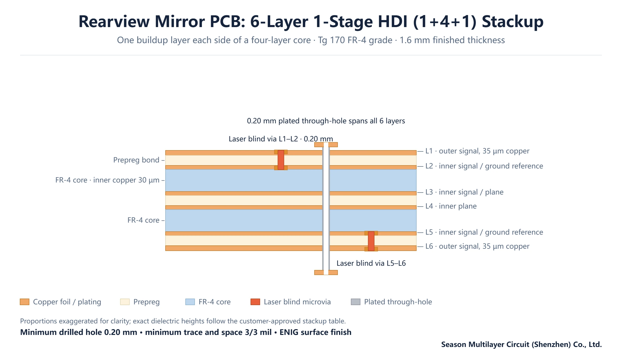
The notation 1+4+1 reads from the outside in: one buildup layer on top, a four-layer core in the middle, and one buildup layer on the bottom. The core sub-board is laminated first with conventional prepreg and FR-4 cores; the outer buildup layers are pressed afterwards and drilled with laser microvias that connect the outer surface to the first inner layer only.
| Layer | Function | Interconnect structure |
|---|---|---|
| L1 | Outer signal and component pads | 1-stage laser blind via down to L2 |
| L2 | Inner signal / ground reference | First landing layer for the blind via |
| L3 | Inner signal / plane | Core layer |
| L4 | Inner plane | Core layer |
| L5 | Inner signal / ground reference | Core layer |
| L6 | Outer signal and component pads | 1-stage laser blind via up to L5 |
Because the blind vias span exactly one dielectric, they can be small, placed densely, and filled reliably. Everything that must cross the full board still uses 0.20 mm plated through-holes, which the fabricator drills mechanically in the same panel. The stackup stays symmetric about the center of the board, which is what controls bow and twist through lamination: an asymmetric copper or dielectric distribution is the most common root cause of warped mirror boards that fail pick-and-place later.
Impedance Control and Reference Planes
A mirror module mixes three signal classes on one board: a high-speed camera link, general-purpose digital buses, and power distribution. Each class wants a different controlled impedance, and the stackup has to deliver all of them from the same six layers. The single-ended and differential pairs are referenced to the adjacent plane layers, which is why L2, L4 and L5 are assigned reference duty in the stackup table above.
Production tolerance is what separates a usable quote from a spec sheet that looks good but fails in the factory. The standard windows are ±10% for single-ended traces, ±8% for differential pairs, and ±5% where a design genuinely needs the tight window, such as the camera SerDes pair. Anything tighter than ±5% moves the board out of standard process capability and should only be specified when the interface standard truly demands it.
Verification happens on a test coupon processed in the same panel as the production boards, measured by TDR before shipment. Ask your supplier to include the coupon data with the first articles; it converts impedance from a promise into a measured number, and it gives your hardware team a baseline for comparison when the design spins.
Design Rules for 0.20 mm BGA Escape
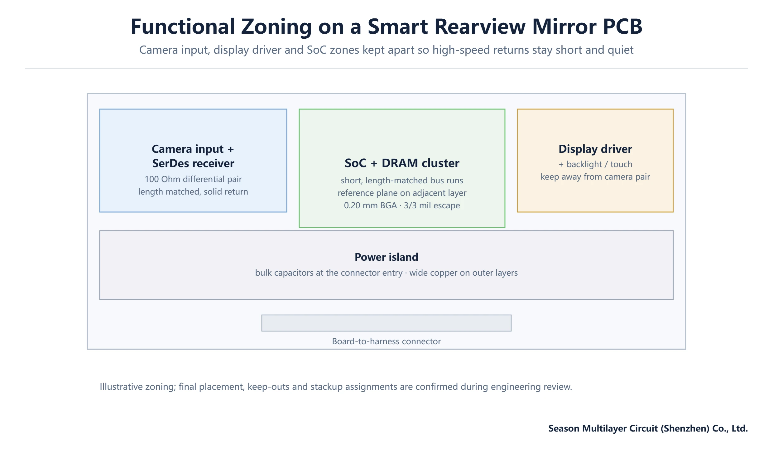
The processor on a smart mirror typically lands in a 0.20 mm pitch BGA. With a 1-stage blind via and a 3/3 mil trace window, the escape pattern works without buried-via complexity: inner rows fan out on the blind via to L2, then route on the first inner layer, while the outer rows escape on the surface. The figure below shows how the functional zones sit around that escape field.
Three rules keep the layout manufacturable on the first pass:
- Keep the camera SerDes pair on the shortest possible path from the connector to the receiver, with an unbroken reference plane underneath; every layer change adds a return path to fix.
- Place bulk decoupling where power enters the board, not beside the BGA; the 30 µm inner copper carries distribution currents comfortably when the loop is short.
- Reserve 0.20 mm hole-to-copper clearance around every plated through-hole; cramming traces against the PTH pad is the most frequent cause of etch Shorts flagged at engineering review.
If your layout already violates one of these, a DFM pass before release is cheaper than a respin; the PCB DFM analysis checklist lists what a fabricator reviews in the first 24 hours.
Automotive Reliability Requirements on a Rearview Mirror PCB
A mirror module lives in a hostile corner of the vehicle: it sees full sun load in summer, deep cold starts in winter, and constant vibration from the door or windshield mount. The qualification gap between a consumer board and an automotive mirror board is therefore structural, not cosmetic, and it starts with how much copper is left in the hole.
| Aspect | Automotive mirror build | Consumer-grade build |
|---|---|---|
| Operating temperature | −40 °C to +125 °C | 0 °C to +70 °C |
| Hole-wall copper | ≥25 µm | ≥18 µm |
| Qualification testing | Batch temperature cycling, vibration and insulation tests with data kept on file | Sample-based inspection |
| Service expectation | Typically 10–15 years in service | 3–5 years |
| Relative cost | Roughly 1.4–1.8× | 1.0× |
The thicker hole-wall copper is the key detail. Thin copper barrels crack under repeated thermal expansion, and a cracked barrel is an intermittent fault that shows up months after the vehicle is on the road. On this build class the fabricator verifies hole copper by cross-section on first articles and keeps the data batch by batch, which is also what an IATF 16949-backed quality audit will ask to see.
Materials follow the same logic: the Tg 170 FR-4 grade in this build holds its mechanical properties across the full −40 °C to +125 °C window, and laminates carrying a UL 94 V-0 flammability rating (UL directory check takes minutes) are the default for any interior electronics module. Reliability testing expectations for this class of electronics are codified in IPC qualification standards (IPC standards overview), and your customer-specific requirement usually references one of them.
What Drives the Cost of a 1-Stage HDI Build
Compared with an equivalent through-hole multilayer board, a 6-layer 1-stage HDI build typically lands in the 1.3–1.8× range, and the spread inside that range is explained by four levers. Layer count and finished thickness set the base; the minimum trace and space determines yields on the outer layers; the surface finish adds a fixed premium, with ENIG costing more than OSP but enabling the fine-pitch assembly a mirror module needs; and panel utilization decides how many boards each pressing cycle produces.
The reference build in this article is optimized on the two levers that matter most: the 138 × 162 mm two-up panel keeps utilization high, and the 3/3 mil window avoids the yield penalty of finer geometry. If a quote comes back far above the expected band, the usual suspects are a tighter-than-necessary impedance window, an unnecessary second HDI stage, or a panel arrangement that wastes material. All three are visible in a stackup review before any money changes hands.
Manufacturing and Quality Control Checks
The production flow for this build differs from a standard multilayer board in exactly two places: the extra lamination cycle for the buildup layers, and the laser drilling step for the blind vias. Everything else — imaging, plating, solder mask, legend, routing and electrical test — runs on the same equipment as a conventional 6-layer board, which is why cycle times stay close to standard multilayer lead times.
Inspection is where a mirror module earns its reliability rating. Every board passes automated optical inspection on each copper layer, followed by 100% flying-probe or fixture testing of the electrical network. First articles are cross-sectioned to confirm hole-wall copper and blind-via landing quality, and the sections are archived. Batch test reports travel with the shipment so incoming inspection at your side can verify without re-testing.
Traceability closes the loop: each panel carries a serial that links the board back to its material lots and process records. If a field issue ever reaches the fabricator, the affected batch can be isolated within hours instead of weeks — a small administrative detail that automotive customers increasingly treat as a purchase requirement.
Sourcing a Rearview Mirror PCB: Files and Lead Times
A fabricator can quote this board class from four inputs: Gerber data including the drill files, the intended stackup, the impedance table, and the assembly-related requirements such as surface finish and solder mask color. Supplying them together removes a full round of clarification emails. Season PCB maintains a dedicated product page for this exact class — the 6-layer HDI rearview mirror PCB — with the build details above already configured.
Prototype lead time for a 6-layer 1-stage HDI build typically runs 5–7 working days and production batches around 15–20 working days, both confirmed at engineering review rather than promised blindly. Volume capacity is not the constraint in this class: the group operates three plants with an annual capacity of 3,000,000 m² across 2–30 layer counts, so scaling from mirror prototypes to full production is a scheduling exercise, not a requalification.
- Send Gerbers plus stackup intent; flag any impedance class above ±8% so it is engineered in from the start.
- Request first-article cross-sections for hole copper and blind-via landing as part of the quote, not after.
- Agree the batch documentation package (test reports, coupon TDR data) before production release.
For a wider view of how this board sits in the vehicle architecture, the automotive electronics PCB guide covers material and process selection across cockpit domains, and the 6-layer automotive PCB prototype page shows the adjacent build class used for domain controllers.
Frequently Asked Questions
What does 1+4+1 mean on a 6-layer 1-stage HDI PCB?
It describes the construction sequence: a four-layer core sub-board is laminated first, then one buildup dielectric is pressed onto each outer surface. The single buildup pair per side is what makes the board 1-stage — one laser drilling pass connects each outer layer to the adjacent inner layer, and no microvia spans two dielectrics.
Why does a rearview mirror PCB use HDI instead of a standard multilayer board?
The processor in a smart mirror sits in a 0.20 mm pitch BGA, and a through-hole stackup cannot escape that pitch without via-in-pad structures or much larger boards. One stage of laser blind vias provides the escape density, keeps lamination cycles low, and holds the finished board at 1.6 mm for the housing mechanics.
What files do I need to get a rearview mirror PCB quoted?
Gerber data with drill files, the intended stackup, the impedance table with tolerance classes, and assembly requirements such as surface finish. With those four inputs a fabricator can return a complete process review and price; missing stackup or impedance data is the usual cause of quote delays.
Which surface finish is used on automotive mirror modules?
ENIG is the default. It leaves a flat, gold-capped pad that suits fine-pitch BGA assembly and the board-to-board or FPC connectors commonly found in mirror modules, and it does not oxidize during storage. OSP can be used for cost-driven builds, but it is less forgiving on multiple reflow passes.
How is impedance controlled on a 1-stage HDI build?
The stackup assigns reference planes adjacent to each routing layer, and production holds ±10% on single-ended traces, ±8% on differential pairs, and ±5% for critical links such as camera SerDes. Compliance is verified by TDR measurement on a coupon processed in the same panel, with data supplied alongside first articles.
What reliability tests apply to an automotive mirror board?
Typical batch verification covers temperature cycling across the −40 °C to +125 °C service window, vibration, and insulation resistance, with cross-sections confirming hole-wall copper of 25 µm or more. The manufacturing quality system runs under IATF 16949, and test data is archived batch by batch to support customer audits.
How long does a 6-layer 1-stage HDI prototype take?
Prototype builds typically complete in 5–7 working days and production batches in 15–20 working days, both confirmed at engineering review once the Gerbers have been checked. Complex impedance requirements or non-standard materials add review time, so flagging them in the first message keeps the schedule honest.
Get Your Rearview Mirror PCB Stackup Reviewed
Send your Gerber data and stackup intent for a process review before release: the engineering team confirms impedance windows, BGA escape feasibility and panelization in one pass, so the quotation you receive reflects a build that will run on standard tooling. The automotive HUD PCB page covers the neighboring display-board class if your module drives the instrument cluster as well.
Planning a Rearview Mirror PCB? Send It for Engineering Review
The fastest next step is to submit your Gerber package and stackup intention for engineering review. You get feasibility comments on trace and space, via structure and material selection, matched to the reference 6-layer HDI rearview mirror PCB described above, and any spec outside the process window is called out before quoting.