Book Appointment Now

A plain-English guide to the multilayer PCB: how cores, prepreg and copper foil bond into one board, plus a full 6-layer stackup example.
What Is a Multilayer PCB? Layers, Stackup and Uses Explained
A multilayer PCB is inside almost every product you quote: the industrial controller, the car display, the storage carrier, the security terminal. Yet the vocabulary around it — cores, prepreg, copper foil, layer counts — often gets fuzzy between a buyer and a factory, and that fuzziness costs money when a stackup has to be redone. This guide gives you the plain-English definition, a real 6-layer stackup with thicknesses, and the decision logic for when layers actually pay off.
You will learn how a multilayer PCB is laminated from copper-clad cores and prepreg, how it differs from single-sided and double-sided boards, which applications justify 4 to 30 layers, and what drives cost and yield before you commit a design to production.
Table of Contents
- What Is a Multilayer PCB?
- How a Multilayer PCB Stackup Is Built
- Multilayer PCB vs Single-Sided and Double-Sided Boards
- Reference 6-Layer Multilayer PCB Stackup (1.0 mm)
- When a Design Needs More Than Two Layers
- Common Multilayer PCB Applications
- Design Rules That Protect Multilayer PCB Yield
- What Drives Multilayer PCB Cost
- Choosing a Multilayer PCB Manufacturer
- FAQ
- Get Your Multilayer PCB Stackup Reviewed Before You Commit
What Is a Multilayer PCB?
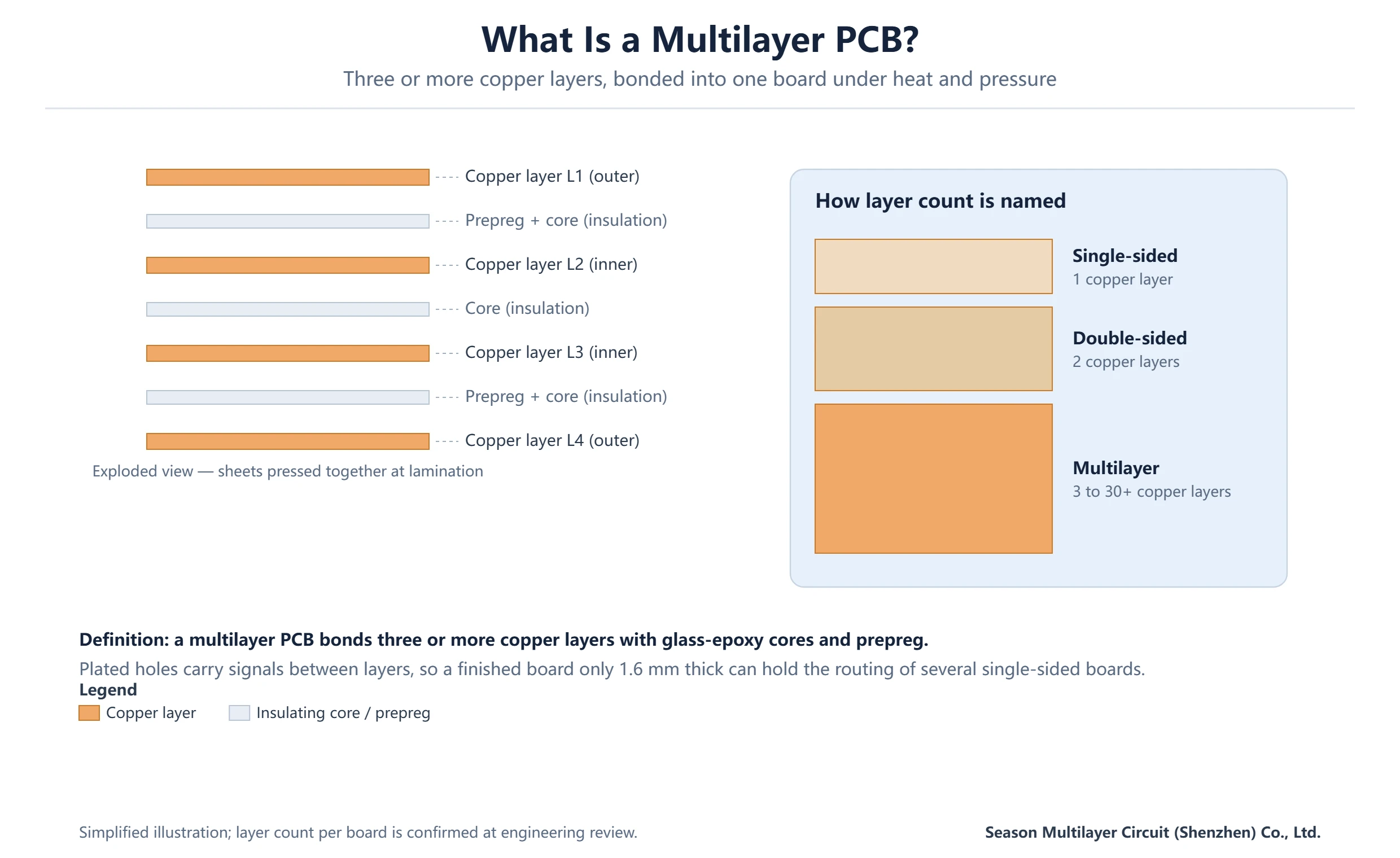
A multilayer PCB is a printed circuit board that bonds three or more copper layers into a single rigid board. The copper layers carry signals and power; glass-epoxy cores insulate them from each other; and prepreg — a semi-cured glass fabric pre-impregnated with resin — glues the whole sandwich together under heat and pressure. Plated through holes and buried vias carry connections between the layers, which is what makes the stack electrically useful rather than just physically thick.
The practical definition that matters at a factory is the copper count. One copper layer is a single-sided board, two is double-sided, and from three upward the board is laminated in presses rather than simply etched and drilled. That lamination step changes everything about how the board is planned: layer order, copper balance and material selection have to be agreed before fabrication, not after.
How a Multilayer PCB Stackup Is Built
Most 4-to-12-layer boards use foil lamination. The inner layers do not start as separate etched sheets — they start as copper foil bonded to both faces of a rigid core. A 6-layer board typically uses two such copper-clad cores: the inner four layers (L2–L5) are the foils and laminate of those cores. The outer layers are then formed by pressing copper foil against prepreg on each side during the lamination cycle.
The cross-section below shows the result: two 0.30 mm cores carrying the inner copper, prepreg bonds of different glass styles between them, and outer foils plated up to final thickness. A PTH connects all six layers, while a buried via inside the first core connects L2 to L3 without using any space on the outer layers.
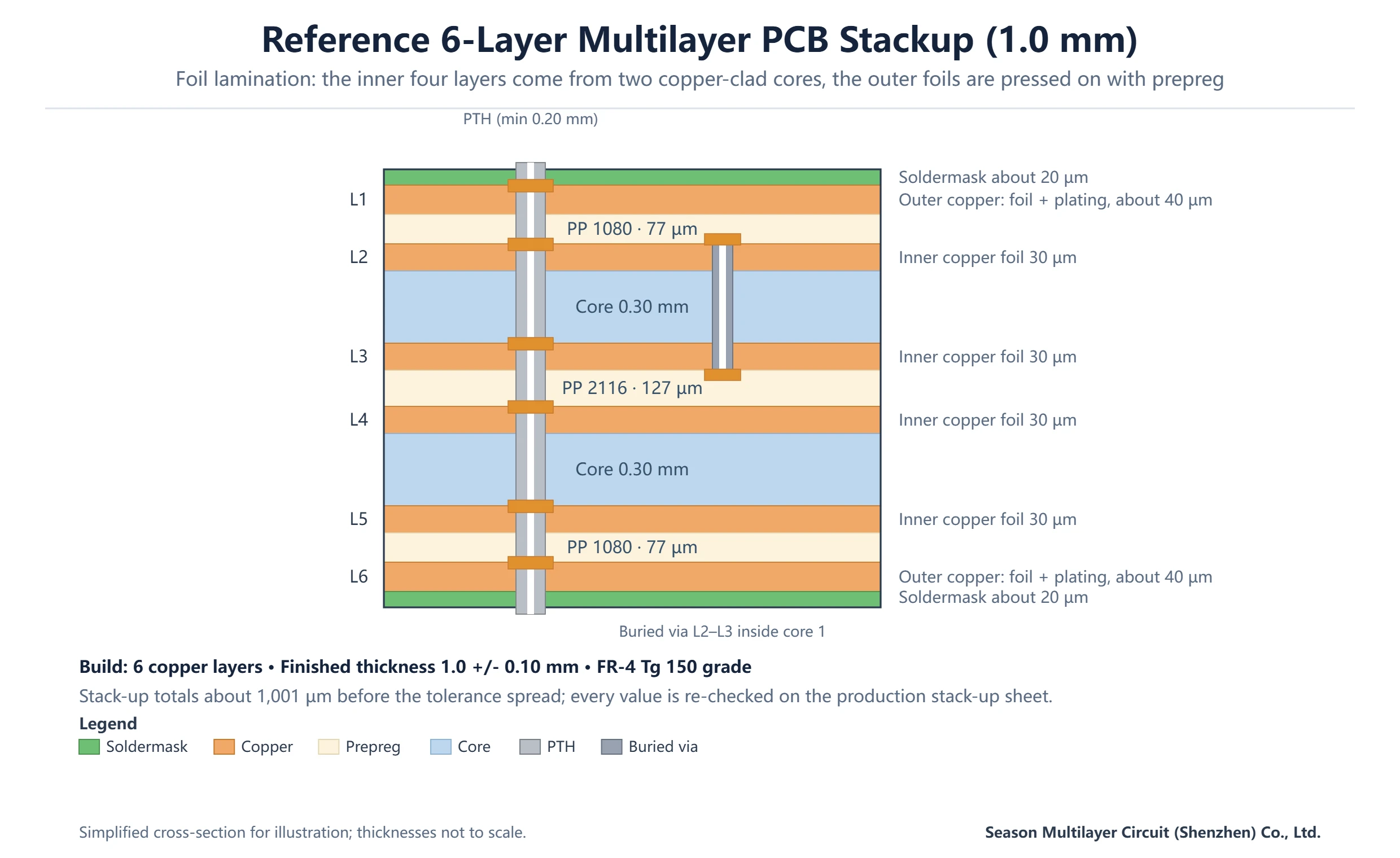
One rule survives every project: keep the stackup symmetric about the centerline. Copper weight, core thickness and prepreg style should mirror from top to bottom, because an asymmetric press cools unevenly and the board warps. The lamination step itself is where this is decided — you can see how it fits into the full process in our PCB lamination process guide.
Multilayer PCB vs Single-Sided and Double-Sided Boards
The three board families are not ranked by prestige — each fits a different routing problem. The table below puts them side by side:
| Board type | Copper layers | Routing character | Relative cost per board |
|---|---|---|---|
| Single-sided | 1 | Low density; traces on one face only, jumpers often needed | Baseline |
| Double-sided | 2 | Moderate density; PTHs connect both faces | Slightly above baseline |
| Multilayer | 3 to 30+ | High density; dedicated ground and power planes possible | Higher, scaling with layer count |
A double-sided board remains the right answer for simple power supplies, LED drivers and relay logic. The moment a design adds a fine-pitch processor, mixed analog and digital sections, or an impedance-controlled interface, routing it on two layers turns into a maze of jumpers and fragile returns — that is the point where moving to a multilayer PCB is cheaper than debugging the two-layer version.
Reference 6-Layer Multilayer PCB Stackup (1.0 mm)
Here is a production stackup for a 1.0 mm finished 6-layer board, the kind used in storage carriers and compact control modules. Reading it from the top down makes foil lamination concrete:
| Layer | Material | Thickness | Role |
|---|---|---|---|
| Soldermask | Epoxy ink | about 20 µm | Both outer faces |
| L1 | Copper foil + plating | about 40 µm | Outer signal |
| Prepreg | 1080 glass style | about 77 µm | Bonds foil to core |
| L2 | Copper foil | 30 µm | Inner signal |
| Core | FR-4 laminate, Tg 150 grade | 0.30 mm | Carries L2 and L3 foils |
| L3 | Copper foil | 30 µm | Inner signal |
| Prepreg | 2116 glass style | about 127 µm | Bonds the two cores |
| L4 | Copper foil | 30 µm | Inner signal |
| Core | FR-4 laminate, Tg 150 grade | 0.30 mm | Carries L4 and L5 foils |
| L5 | Copper foil | 30 µm | Inner signal |
| Prepreg | 1080 glass style | about 77 µm | Bonds foil to core |
| L6 | Copper foil + plating | about 40 µm | Outer signal |
The stack adds up to roughly 1,001 µm before tolerances, landing on the 1.0 mm ± 0.10 mm target. Note where the thickness actually lives: the two cores contribute 600 µm — most of the board — while prepreg choices tune the remaining gap. That is why a factory asks for your finished thickness and your impedance targets together: changing one 1080-to-2116 swap shifts both.
When a Design Needs More Than Two Layers
Layer count is not a status symbol; it is a response to specific constraints. You genuinely need the extra layers when one or more of these apply:
- Fine-pitch escape. A 0.4 mm or 0.5 mm pitch BGA needs inner-layer fanout that two faces cannot provide.
- Dedicated ground planes. Return currents need an unbroken reference; a plane layer under every signal layer is the cheapest fix.
- Impedance control. USB, Ethernet, DDR and RF lines hold their impedance only with a defined dielectric height above a plane.
- Crosstalk separation. Sensitive analog lines and fast digital edges want their own spacing layers.
- Board size limits. When the enclosure fixes the outline, density has to grow inward instead of outward.
If none of these apply, staying at two layers is the honest engineering answer. The failure pattern we see most often is a design that adds a fourth layer “for safety” without assigning it a job — an unused plane that only adds lamination cost. Every layer should earn its place.
Common Multilayer PCB Applications
Layer counts cluster by application, because each product family solves a similar routing problem:
| Application family | Typical layers | Why layers help |
|---|---|---|
| Industrial control and automation | 4–10 | Dense I/O with clean returns for mixed signals |
| Automotive cabin modules (instrument clusters, mirrors, displays) | 4–12 | Space limits plus stable operation over temperature |
| Storage and computing carriers (SSD boards, core boards) | 6–14 | Fine-pitch BGA escape and impedance-controlled data buses |
| Security and intelligent terminals | 8–12 | Isolation between video, radio and power sections |
| High-speed and RF designs | 4–12 | Reference planes for controlled impedance |
Two production examples show the range. An 8-layer security system PCB uses its stack to separate video capture, network and power sections; a 12-layer 1-stage HDI core board combines conventional inner layers with a build-up stage for a dense processor escape. Same lamination discipline, very different layer assignments.
Design Rules That Protect Multilayer PCB Yield
Three habits keep a multilayer stack buildable. First, balance copper: distribute copper weight symmetrically about the centerline so the press pulls evenly from both sides — our guide to balanced stackup design and warpage control covers the 0.75% bow-and-twist ceiling that Class 3 work demands.
Second, plan impedance from the stack, not after it. Trace width alone does not set impedance; the dielectric height and the plane underneath do. The stackup design rules article shows how signal, plane and prepreg choices interact, and why a coupon is tested on every impedance-controlled panel.
Third, respect lamination mechanics: symmetric press openings, resin content matched to the copper fill, and drilled stack tolerances that the plating can actually follow. The acceptance criteria for the finished board come from IPC-6012 and IPC-A-600 — the IPC standards library is the authoritative reference for both.
What Drives Multilayer PCB Cost
Without quoting a single number, the cost structure of a multilayer PCB is predictable. These drivers dominate, in rough order of impact:
| Cost driver | How it moves the price |
|---|---|
| Layer count | Each added layer brings more material, more press openings and more inspection surface |
| Material grade | Tg 150 and Tg 170 FR-4 grades sit close together; low-loss and high-frequency styles cost noticeably more |
| Finished thickness | Thicker cores and heavier copper raise laminate cost before processing starts |
| Surface finish | ENIG, OSP and HASL carry different relative costs per panel |
| Impedance control | Tighter tolerances add coupon testing and process control, not just design effort |
The relative logic matters more than any single quote: moving a 4-layer design from a standard build to one extra lamination cycle typically raises cost by double-digit percentages, while changing surface finish on the same stackup moves it by only a few percent. We break the 4-layer case down fully in the 4-layer PCB cost drivers checklist.
Choosing a Multilayer PCB Manufacturer
Because the stackup is committed at lamination, your best protection is a factory that reviews it before the press runs. When you compare suppliers, look for: documented capability at your layer count, an engineering review that returns concrete stackup feedback, quality system certification (ISO 9001:2015 and IATF 16949 for automotive work), and the willingness to say “this layer is unnecessary”. Our multilayer PCB manufacturer selection checklist turns those points into a scorecard.
Scale matters too. 998 PCB Group, the manufacturing group behind Season PCB, was founded in 2006 and produces 3,000,000 m² of boards per year across plants in Shenzhen, Jiangxi and Anhui, covering 2 to 30 layers from standard FR-4 through HDI builds. That depth matters when a design migrates from a 6-layer prototype to volume production on the same stackup documentation.
Finally, send clean data. Fabricators work from your Gerber data, drill files and stackup table — a clearly named layer set shortens the engineering review and removes the most common source of first-article surprises.
Frequently Asked Questions
How many layers can a multilayer PCB have?
There is no fixed ceiling, but common products sit between 4 and 14 layers. Production capability at our facilities spans 2 to 30 layers, with designs above roughly 14 layers reviewed per project for lamination and registration feasibility. Most cost-optimal designs land in the 4-to-10-layer range, where each layer has a clear job.
What is the difference between a multilayer PCB and an HDI PCB?
They describe different axes. Multilayer refers to the number of bonded copper layers; HDI (high density interconnect) refers to how layers connect — laser microvias, fine lines and build-up stages instead of only mechanical drilled holes. The two combine freely: a 6-layer 1-stage HDI board is a multilayer PCB that uses laser-drilled blind vias on top of a conventional core.
What materials are used in a multilayer PCB?
The standard kit is FR-4 cores (commonly Tg 130 to Tg 180 grades), matching prepreg glass styles such as 1080 and 2116, and electrodeposited copper foil. High-frequency designs swap in low-loss laminates with defined dielectric constants, while the copper, plating and soldermask chemistry stay broadly the same. Material selection is always confirmed against your operating temperature and signal speed.
How thick is a typical multilayer PCB?
Most consumer and industrial builds finish between 0.8 mm and 2.0 mm. The 6-layer example in this article lands at 1.0 mm ± 0.10 mm, and a conventional 4-layer board typically finishes near 1.6 mm. Thickness is tuned through core and prepreg selection, so it should be specified together with impedance targets rather than as an afterthought.
Why do multilayer PCBs cost more than 2-layer boards?
Three factors stack up: more raw material (cores, prepreg and copper per panel), additional lamination cycles that consume press time, and more inspection surface per panel. The premium is not linear — going from 2 to 4 layers is a modest step, while each layer beyond 8 costs proportionally more because yields tighten. Relative multipliers are confirmed per design at engineering review.
Can a multilayer PCB be repaired if an inner layer is damaged?
Practically, no. Inner-layer traces sit between laminated cores where no tool can reach, so a defect in an internal layer scrapes the panel. Rework is limited to outer-layer features: patching a trace, reflowing a joint or fixing soldermask. This is exactly why inner-layer inspection happens before lamination, when defects can still be caught cheaply.
How long does a multilayer PCB prototype take?
For common 4-to-8-layer builds, prototype lead time typically falls between one and two weeks depending on material availability and stackup complexity; HDI constructions add laser drilling and extra lamination cycles. Every order is confirmed at engineering review before the schedule is promised, which keeps the quoted date realistic.
Get Your Multilayer PCB Stackup Reviewed Before You Commit
Send your Gerber files and target impedance, and our engineering team will return a concrete read on layer assignment, core and prepreg selection, copper balance and panel utilisation — before anything is pressed. If a layer can be removed or a material downgraded without hurting performance, the review will say so.
Start from the PCB manufacturing services overview or browse more guides in the PCB basics library to see how the full process fits together.