Book Appointment Now

A buyer's guide to the 6-layer 1-stage HDI kids smartwatch PCB: stackup, specifications, microvia reliability and the DFM checks to run before release.
Kids Smartwatch PCB: 6-Layer 1-Stage HDI Stackup and Specs
A kids smartwatch PCB packs a SoC, power management, GNSS, a cellular or Bluetooth radio and a display interface into a board small enough to sit on a child’s wrist. The usual failure mode is not a exotic material or a fancy finish; it is routing density: a 0.2 mm pitch SoC on a roughly 40 mm board with four radios competing for space. When a two-layer or four-layer through-hole build runs out of escape routing, the project slips and the board grows until it no longer fits the case.
This guide walks through the reference build we produce for this exact application: a 6-layer 1-stage HDI stackup (1+4+1) on Tg 150 FR-4 grade laminate, 0.8 mm thick, with 0.10 mm laser microvias and ENIG finish. You will get the full specification table, a comparison against through-hole boards, the microvia reliability chain, and the design rules and inspection points that keep a wearable PCB design out of rework.
Table of Contents
- What Is a Kids Smartwatch PCB?
- The 1+4+1 Stackup Behind a Kids Smartwatch PCB
- Kids Smartwatch PCB Specifications at a Glance
- Why 1-Stage HDI Beats a Through-Hole Board in a Watch
- Microvia Reliability: Resin Fill and Cap Plating
- Design Rules That Prevent Wearable PCB Rework
- Antenna and RF Layout on a Small Board
- Quality Control from First Article to Volume
- Prototype Lead Times and Scaling to Volume
- FAQ
- Get Your Kids Smartwatch PCB Reviewed Before You Commit
What Is a Kids Smartwatch PCB?
A kids smartwatch PCB is the main carrier board of a children’s wearable: it hosts the application processor, memory, power management, Bluetooth or 4G cellular module, GNSS receiver, motion sensors and the charge and display connectors. Compared with an adult smartwatch, kids’ models usually add a cellular radio for calls and location tracking, which increases layer count and radio complexity at the same time.
The dominant constraint is area, not thickness. A typical watch main board measures a few tens of millimetres per side and must break out a 0.2 mm pitch BGA on its outer layers while keeping an antenna region clear of copper. Our 6-layer 1-stage HDI kids smartwatch PCB is built to exactly this construction, and it is the reference point for every figure in this article.
For buyers, three consequences follow. First, laser microvias are not optional: mechanical drills cannot reach the escape density a 0.2 mm pitch BGA needs on a board this small. Second, the stackup must stay symmetric, because a warped board will not survive automated assembly in a watch case. Third, the finish and pad design must tolerate hundreds of charge-connector mating cycles and humid wrist environments.
The 1+4+1 Stackup Behind a Kids Smartwatch PCB
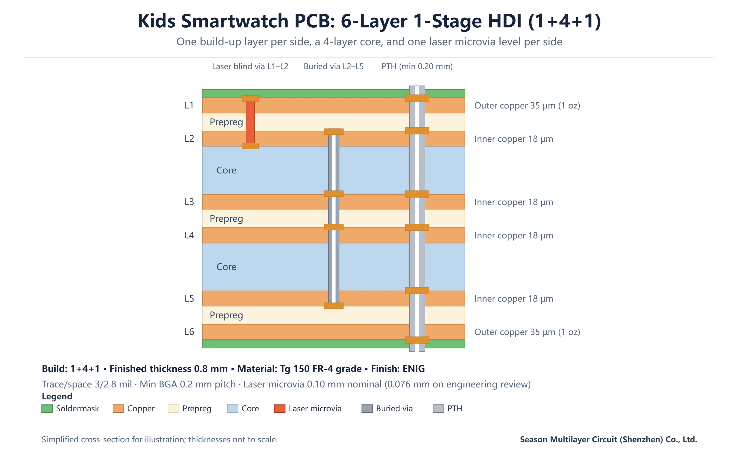
The notation 1+4+1 describes the lamination structure. The core is a conventional 4-layer sub-board: two inner copper pairs (L2/L3 and L4/L5) bonded around two cores with prepreg in between. One build-up layer is then laminated onto each outer face, giving the final six copper layers. One lamination cycle for the inner sub-board, one more for the build-up, two cycles in total.
That single build-up step is what makes the board 1-stage HDI. Each outer layer connects down to the adjacent inner layer through a laser blind microvia: L1 to L2 on top, L6 to L5 on the bottom. The inner sub-board carries a mechanically drilled buried via from L2 to L5, and a plated through hole spans all six layers for connectors, shielding clips and test points. Deeper interconnect detail on how these via types compare is covered in our HDI PCB vs standard PCB guide.
The reference material is a Tg 150 FR-4 grade, a mid-Tg laminate that balances cost, drillability and dimensional stability at 0.8 mm finished thickness. Going thinner is possible but squeezes the aspect ratio of the buried via, so we treat anything below 0.8 mm as an engineering-review item rather than a catalogue option. Symmetry is preserved top to bottom, which is what keeps post-assembly warpage inside assembly tolerances.
Kids Smartwatch PCB Specifications at a Glance
The table below lists the parameters of the reference build exactly as they appear on the product page. Treat it as a sanity check for your own stackup: if your design asks for less than these limits, a standard through-hole vendor may quote it; if it asks for more, you are in 2-stage territory and the cost model changes.
| Parameter | Reference value |
|---|---|
| Layer count | 6 layers, 1-stage HDI (1+4+1) |
| Base material | Tg 150 FR-4 grade (Mid-Tg) |
| Finished thickness | 0.8 mm |
| Outer copper | 35 µm (1 oz) |
| Inner copper | 18 µm (0.5 oz) |
| Laser microvia | 0.10 mm nominal; 0.076 mm on engineering review |
| Minimum mechanical via | 0.20 mm |
| Trace / space | 3 / 2.8 mil |
| Minimum BGA pitch | 0.2 mm |
| Surface finish | ENIG |
| Reference panel | 141.8 × 77.8 mm panel, 8 boards up |
Two rows deserve comment. The 3/2.8 mil trace and space is the budget that makes a 0.2 mm pitch BGA fan out on the outer layers; anything finer moves the board toward 2-stage HDI and mSAP-class processes. And the 8-up panel size is why unit cost drops sharply at volume: a watch board is small, so panel utilisation, not board complexity, is often the bigger cost lever once the design is stable.
Why 1-Stage HDI Beats a Through-Hole Board in a Watch
A 4-layer or 2-layer through-hole board is cheaper per square metre, and for a toy-grade band without a cellular radio it is often enough. The moment you add GNSS plus 4G plus a display interface, escape routing around the SoC consumes every spare square millimetre, and the comparison flips. The table summarises where the two constructions actually differ.
| Dimension | 1-Stage HDI (1+4+1) | 2–4 layer through-hole |
|---|---|---|
| Interconnect | Laser blind vias L1–L2 and L5–L6, buried via L2–L5 | Through holes only |
| Minimum via | 0.10 mm laser; 0.20 mm mechanical | 0.20 mm and larger |
| Fine-pitch support | 0.2 mm BGA fans out on 3/2.8 mil rules | Escape routing congests quickly |
| Routing density | High; frees board area for antenna keep-outs | Limited; forces a larger board |
| Relative cost factor | Roughly 1.3–1.8× | 1.0× |
| Typical fit | Cellular + GNSS smartwatch main boards | Basic bands, accessory boards |
The cost factor is a multiplier, not a quote: the actual figure depends on layer count, yield and panel utilisation, and it shrinks at volume because an HDI panel carries more boards than a through-hole panel of the same size. In practice the decision rule is simple: if the through-hole version forces the board above the case’s internal volume, 1-stage HDI is the cheaper path to a shippable product, because mechanical redesign costs more than the board premium.
Microvia Reliability: Resin Fill and Cap Plating
A 0.10 mm laser via is only as good as its fill. In the high-density zones of a kids smartwatch PCB, blind vias are resin-filled and then capped with plated copper, so the pad stays solid during reflow. An unfilled or voided microvia can wick solder up the barrel, starve the joint and, on a thin 0.8 mm board, lift the pad under probe or assembly stress.
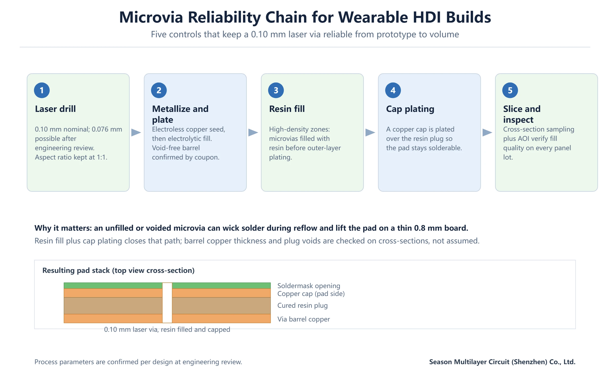
The chain runs laser drill, metallise and plate, resin fill, cap plating, then slice inspection. We keep the microvia aspect ratio at 1:1, which is the single most effective guard against incomplete plating. Fill quality is verified on cross-sections per lot, not assumed from process recipes; barrel copper thickness and plug voids are the two items we photograph and archive.
If you are weighing plug materials for your own stack, our comparison of resin plugging versus solder-mask ink plugging explains when each is the right choice and what each costs in added process steps.
Design Rules That Prevent Wearable PCB Rework
Most wearable boards that come back for a second spin fail on a handful of recurring items. These are the rules we apply at DFM review before any kids smartwatch PCB panel is cut, and they are worth self-checking before you release Gerber:
- Keep every laser microvia at or below a 1:1 aspect ratio; on a 0.8 mm build that means one build-up layer per side, not two.
- Budget 3/2.8 mil trace and space on the outer layers so the 0.2 mm pitch BGA escapes without dogbone congestion.
- Reserve the antenna region early: keep-outs near the strap end must stay free of copper, including pour, on every layer.
- Hold the stackup symmetric about the centre so warpage stays within assembly limits after reflow.
- Specify ENIG for the fine-pitch pads; HASL cannot flatten enough for 0.2 mm pitch parts.
- Send the stackup with the Gerber package so impedance and copper balance are checked before lamination, not after.
The last item matters more than it looks. Our PCB manufacturing services include a free DFM and stackup review before cutting, and on wearable projects it routinely catches antenna keep-out violations and copper-balance asymmetries that would otherwise surface as warped panels or failed radio tests.
Antenna and RF Layout on a Small Board
A cellular kids watch runs Bluetooth, GNSS and often a 2G/4G cellular front end on one board, so coexistence is a layout problem as much as a stackup problem. Each antenna needs a keep-out at the board edge, and each feed wants a short, straight run over an unbroken ground plane on the adjacent inner layer. Radio performance also has to survive type-approval testing by bodies such as UL Solutions, which is one more reason the antenna region deserves its own layout pass rather than leftover space.
The 1+4+1 stackup helps here: L2 and L5 sit directly under the outer routing layers and act as reference planes, so RF returns have a short path and the digital section can be grounded without crossing the radio’s return currents. Place the radio module and its filters first, then the SoC and memory, then power; that ordering keeps the noisy switching regulators away from the antenna end of the board.
Two practical warnings from production experience. A metal shield can placed too close to the antenna detunes it and shifts the match after assembly, so model the can in the layout, not just the board. And the battery and its flex sit millimetres from the feed on most watch designs; keep the battery return path out of the ground the RF front end references, or coexistence measurements will drift between boards.
Quality Control from First Article to Volume
Because a smartwatch board hides its worst defects under the shield can and the battery, inspection has to happen at the panel stage. The reference flow combines full-panel automated checks with per-lot destructive sampling, as summarised below.
| Check | Method | What it catches |
|---|---|---|
| Outer-layer defects | AOI on every panel | Opens, shorts, width violations on 3/2.8 mil routing |
| Electrical continuity | Flying probe or fixture test, 100% | Barrel voids and net opens invisible to AOI |
| Microvia quality | Cross-section per lot | Resin fill voids, thin barrel copper, cap plating gaps |
| Impedance | Coupon TDR per panel | Drift in 50 ohm single-ended RF feeds |
| Final visual and thickness | Sample per panel | Soldermask coverage, ENIG quality, 0.8 mm thickness |
First-article confirmation locks the process before volume: the same engineering parameters travel with the job from prototype to repeat orders, so a batch-five board matches the sample you approved. Acceptance criteria reference IPC class 2 workmanship, with class 3 available on request; the governing documents are indexed on the IPC standards page. Test reports and slice data are archived per batch, which is also what an auditor will ask to see if your program carries a safety or telecom certification.
Prototype Lead Times and Scaling to Volume
For the reference 6-layer 1-stage build, prototype runs complete in roughly 5–7 working days and volume runs in 15–20 working days, with the exact schedule confirmed at engineering review once the stackup and panel are fixed. Those ranges assume a complete Gerber package; missing impedance or drill data is the most common cause of a slipped start date.
Volume ramping is a group-level strength: production spans three plants in Shenzhen, Jiangxi and Anhui with a combined capacity of 3,000,000 m² per year across 2–30 layer technologies, so a seasonal spike in watch orders does not queue behind unrelated products. Because the reference panel carries eight boards, unit cost steps down noticeably as volumes move from thousands to hundreds of thousands of pieces.
The same construction family extends to other wearables: a 6-layer 2-stage HDI headphone PCB shares the material system and process controls but adds a second build-up stage for tighter density. If your roadmap includes earbuds or bands alongside the watch, aligning both boards on one stackup platform simplifies qualification and second-source audits.
Frequently Asked Questions
What does 1+4+1 mean in a 6-layer HDI stackup?
It counts the build-up layers around the core: one added copper layer on each face of a 4-layer inner sub-board. The outer pairs connect through 0.10 mm laser blind microvias, the 4-layer core carries a buried via, and the whole board needs two lamination cycles. It is the entry-level HDI construction and the one most smartwatch main boards use.
Can a 0.2 mm pitch BGA fan out on 3/2.8 mil design rules?
Yes. With 3 mil traces and 2.8 mil spaces on the outer layers, a 0.2 mm pitch BGA escapes with straightforward dogbone fan-out on the build-up layers. Going finer than that pushes the design toward 2-stage HDI or mSAP processes, which changes the cost model, so confirm the rules with your fabricator before locking the footprint.
Why is ENIG the default finish for a smartwatch PCB?
ENIG gives a flat, solderable pad that copes with 0.2 mm pitch BGAs and fine-pitch connectors, and its nickel layer resists wear at the charge connector. HASL leaves an uneven dome that complicates fine-pitch assembly. For pads that face repeated mating or corrosion, ENIG also ages more predictably than OSP, which degrades after multiple reflow cycles.
How thin can a 6-layer smartwatch PCB be made?
The reference build is 0.8 mm finished thickness, which fits most watch cases with clearance for the shield can and battery. Thinner builds are possible but compress the buried-via aspect ratio and the power planes, so we treat them as engineering-review items: send the stackup and current draw first, and we will confirm manufacturability before you commit the layout.
What files are needed for a kids smartwatch PCB quote?
A complete Gerber package including drill files, plus the stackup table and, for radio boards, a note of which nets are impedance-controlled. Fabrication drawings help but are not mandatory. With those files, the DFM review returns concrete feedback on microvia density, panel utilisation and cost drivers, and any spec that falls outside standard process windows is flagged before quoting.
How are microvias kept reliable on a thin wearable board?
Three controls: the aspect ratio is held at 1:1, high-density blind vias are resin-filled and capped with plated copper so solder cannot wick into the barrel, and fill quality is verified by cross-section on every production lot rather than assumed. On a 0.8 mm board these controls matter more than anywhere else, because a pad lift there is not repairable.
How long do prototype and volume production take?
Prototype runs for the 6-layer 1-stage reference build complete in roughly 5–7 working days, and volume in 15–20, confirmed at engineering review. The schedule assumes a complete Gerber and stackup package on day one. Volume capacity scales across three group plants with 3,000,000 m² of annual capacity, so ramping from thousands to hundreds of thousands of boards does not require requalification.
Get Your Kids Smartwatch PCB Reviewed Before You Commit
Send your Gerber and stackup for a free DFM review, and you will get back a concrete read on microvia density, panel utilisation and any spec outside standard process windows, before the first panel is cut. The 6-layer 1-stage HDI kids smartwatch PCB page lists the full reference specification and current build options.