Book Appointment Now

What a backplane PCB is and how one is built: thick multi-layer stackups, press-fit connector fields, impedance consistency and backdrilling for stub control.
Backplane PCB Design: Stackup, Connectors and Stub Control
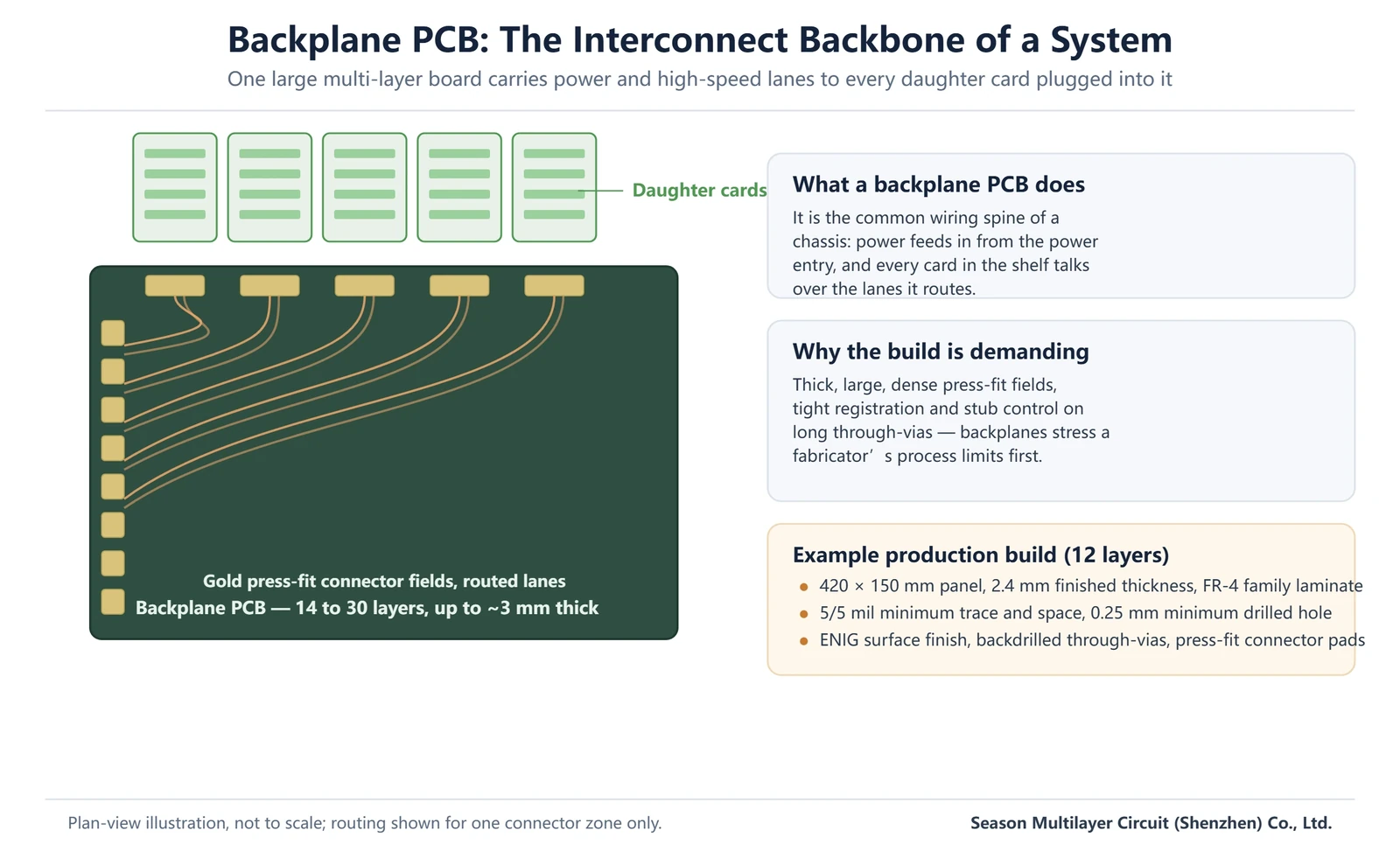
A backplane PCB is the board every other board in a system plugs into. Instead of carrying one product’s logic, it carries the shared wiring spine: power enters through it, and hundreds of high-speed lanes fan out from card slot to card slot across a chassis. Because a single backplane PCB decides whether twenty daughter cards all talk to each other reliably, its build rules sit a step stricter than a conventional multilayer board of the same layer count.
This guide covers what a backplane is and where it is used, and how the stackup differs from a standard build. It explains why connector fields and press-fit zones drive the layout. It closes with why thick boards with long through-vias almost always need backdrilling to control stub resonance.
Those concerns reduce to six rules, developed in order below. Plan the backplane stackup design around paired signal and return layers; hold the press-fit window; apply backdrilling stub control wherever the stack is thick. Keep impedance consistent along the whole route, size power for the whole shelf, and prove all of it at first article on the finished backplane PCB. It closes with an example 12-layer production build and the checks that go with it.
Table of Contents
- What Is a Backplane PCB?
- Where Backplane PCBs Are Used
- Backplane, Midplane and Motherboard: What Differs
- Backplane PCB Stackup: Layers, Thickness and Materials
- Connectors, Slots and Press-Fit Fields
- Stub Control: Why Backplanes Need Backdrilling
- Impedance Consistency Across a Long Backplane
- Power Distribution and Thermal Paths
- Test and Acceptance for Backplane Builds
- An Example 12-Layer Backplane Build
- FAQ
- Plan Your Backplane Build With an Engineering Review
What Is a Backplane PCB?
A backplane PCB is a large, thick, high-layer-count board that carries no signal-processing parts of its own. Its job is interconnection: connectors along its face accept daughter cards, and the copper inside routes power and high-speed signals between those slots. In a 20-slot chassis the backplane replaces what would otherwise be a loom of point-to-point cables, and it does so with controlled impedance on every lane.
Two physical traits separate a backplane from a normal multilayer board. First, size and thickness: backplanes commonly run 14 to 30 layers and several millimetres thick, with outlines measured in hundreds of millimetres, so warpage control and flatness become first-order requirements rather than afterthoughts. Second, the connector fields: dense arrays of press-fit pads concentrate thousands of holes into small regions, which stresses registration, hole quality and pad geometry all at once.
Because the board is the system’s spine, its reliability envelope is the system’s. A marginal via or a warped slot position on a backplane affects every card plugged into it, which is why acceptance criteria and process controls tighten as layer count and slot count rise.
Where Backplane PCBs Are Used
Anywhere a chassis holds a row of pluggable cards, a backplane is doing the interconnect. Telecom and data-center equipment is the classic case: switch and router shelves, server backplanes, and storage systems that aggregate dozens of drives or controllers. Industrial control cabinets use them for the same reason, and test-and-measurement racks depend on them for repeatable signal paths between instruments.
Automotive electronics has joined the list as domain controllers concentrate more functions into one enclosure. A 12-layer high-speed backplane of the kind built here for a vehicle central control system acts as the wiring hub between the modules in the car. It replaces long cable runs with controlled-impedance lanes on a single board.
The common thread across all of these is volume and longevity. For a high-speed backplane the specification work concentrates on the lanes that matter. Identify the SerDes classes early, keep their routes short, and give them the cleanest return paths the backplane stackup design allows. Everything else on the board follows from that plan. Backplanes live in equipment that runs for years, so the build choices that matter are the ones that hold over time. Those choices are plating thickness in the barrel, flatness across the slot row, and connector pad geometry that survives insertion cycles.
Backplane, Midplane and Motherboard: What Differs
Three related terms get blurred in datasheets. A backplane carries connectors on one face and the cards sit parallel to it, perpendicular to the board plane. A midplane moves the connectors to the board’s edge so cards can plug in from both sides, doubling density in the same chassis height at the cost of harder routing. A motherboard, by contrast, carries the processing silicon itself and hosts daughter boards as expansion, so it is a functional board rather than a pure interconnect.
| Attribute | Backplane | Midplane | Motherboard |
|---|---|---|---|
| Connectors | One face, cards parallel to board | Board edge, cards both sides | Socketed on face |
| Own processing silicon | None | None | Yes |
| Typical role | Card-to-card interconnect | High-density card interconnect | System host + expansion |
| Routing freedom | High, full board area | Constrained near edge | Dense, general purpose |
| Build emphasis | Flatness, stub control | Edge registration | General reliability |
The distinction matters for manufacturing because each shape stresses a different process capability. A midplane lives or dies on edge-slot registration; a backplane lives on flatness and via quality across a large panel; a motherboard on ordinary dense-SMT competence. Asking which one your build actually is tells the fabricator which capability page to open first.
Backplane PCB Stackup: Layers, Thickness and Materials
Layer count is set by the lane count and the connector footprint, not by preference. A shelf with 200 differential pairs needs enough signal layers to escape every slot without forcing crosstalk-prone routing, plus solid planes for every voltage domain. That arithmetic is why 14 to 30 layers is the normal working range, and why the stackup is planned around pairing every signal layer with an adjacent return plane before anything else is placed.
Thickness follows from the layer count plus a stiffness requirement. A board hundreds of millimetres long with cards pressing into its connectors cannot flex like a 1.6 mm PCB. Finished thicknesses of 2 to 3 mm and above are typical, often helped by heavier copper in the plane layers. Symmetry still governs: the balanced stackup rules that keep a normal board flat apply with more force here, because a warped backplane misaligns every slot at once. A workable backplane stackup design starts from the slot map, not the other way round. Count the lanes per connector, assign each high-speed class to a layer pair with an adjacent plane, and only then fix the thickness. On a dense shelf this ordering keeps escape routing honest and stops the layer count of a backplane PCB from creeping after layout begins.
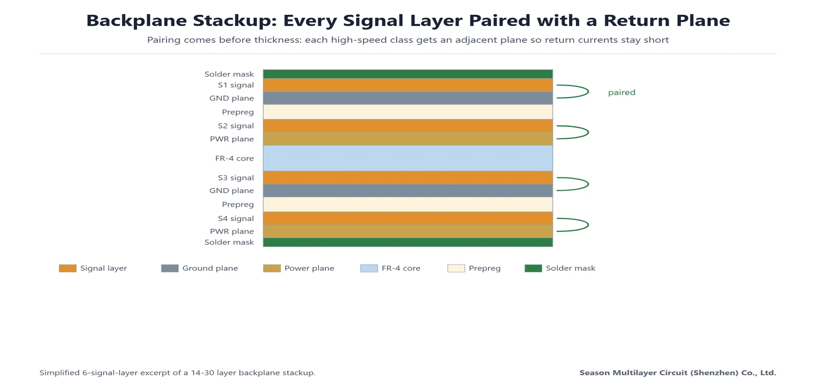
Materials split by signal speed. Conventional FR-4 serves backplanes whose fastest lanes stay within its loss budget. Lanes running multi-gigabit over tens of centimetres justify mid-loss or low-loss laminates on the signal layers. Sometimes this takes the form of a hybrid stackup that keeps the cost of the slower layers down. Power delivery adds its own pressure toward heavy copper planes, since the same board feeds every card in the shelf.
Connectors, Slots and Press-Fit Fields
The connector field is the defining layout feature. High-speed backplanes use press-fit connectors: compliant pins that press into plated holes and form the connection without soldering heat. Press-fit brings real advantages at this scale, including a gas-tight joint that survives insertion cycles and rework without reflowing the whole board. The trade is precision: diameter, plating thickness and pad geometry all sit inside the connector vendor’s window. The field itself places hundreds of these holes in rows.
That concentration is what makes layer-to-layer registration a headline capability for backplane work. Every hole in the field must land inside its pad on every layer of a thick stack. A drift that a normal board would shrug off shows up here as a press-fit hole out of tolerance. Hole quality matters just as much, since the compliant pin forms its joint against the barrel wall itself. A press-fit connector PCB lives or dies by that window. The compliant-pin datasheet fixes a finished-hole diameter and a plating band. The fabricator must hold it across hundreds of holes and every layer of a thick stack, which is why press-fit fields are quoted with registration data attached rather than as a plain drill table.
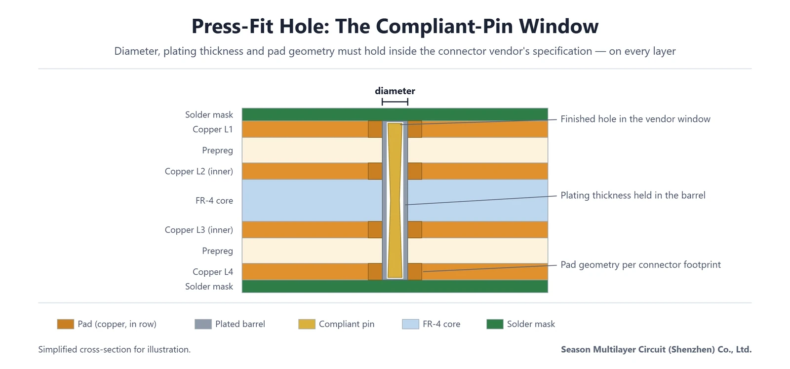
Mechanical design completes the picture. Card guides, stiffeners and mounting holes are part of the board data, and the slot row must stay straight within tight tolerance so the cards seat with the force the connector was designed for. A backplane quote should therefore include the mechanical drawing alongside the electrical data, not treat the board as a rectangle with holes.
Stub Control: Why Backplanes Need Backdrilling
A through-via that connects a signal layer near the board surface continues through the full thickness of the stack below that layer. On a 2.4 mm backplane, the unused portion, the stub, can be longer than the used portion of the same hole. At multi-gigabit data rates the stub behaves as a resonant stub: it reflects energy back into the channel and rings at frequencies that notch the eye diagram. The longer the stub, the lower the frequency at which the damage starts.
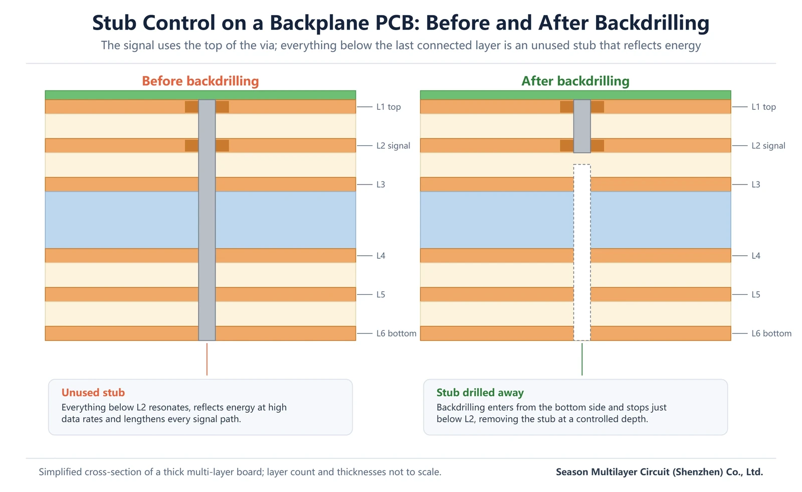
Backdrilling removes the stub. After plating, a slightly larger drill enters from the back side and removes the unused barrel to a controlled depth just below the last layer the signal touches. The depth control is the whole craft: leave too much and the resonance remains, drill too deep and the used connection itself is cut. Treat backdrilling stub control as a stackup deliverable rather than a drill-floor decision. Each hole class carries a depth value derived from the layers it serves, and the values are agreed at engineering review before tooling. When the review owns those numbers, the resonance risk on the backplane PCB is closed on paper instead of in the field. Depth is set per stackup and verified, and the remaining stub is typically held to a length that keeps the resonance above the channel’s operating band.
The backdrilling and signal integrity article covers the mechanism in detail; for backplane work the practical point is to plan for it at stackup time. Signal layers should be placed so stubs are short relative to board thickness. The hole classes that need backdrilling should be identified in the data. The backdrill depth per class should be agreed at engineering review rather than improvised in production.
Impedance Consistency Across a Long Backplane
A lane on a backplane can run hundreds of millimetres from slot to slot, so small impedance errors accumulate over a distance no ordinary board sees. The review question is therefore not only whether the geometry hits the target impedance but whether it holds that target along the whole route. Plane cutouts under connector fields, neck-downs at escape routing and layer transitions all create local dips. A TDR sweep shows these dips as steps.
Tolerances are quoted to match the need: ±10% as the standard production band, with ±8% and ±5% available where the geometry supports the tighter control. The same discipline applies lane to lane. On a high-speed backplane, a few ohms of difference between identical slot positions is visible in the eye margin at the far end. A backplane PCB is therefore judged on consistency across the panel as much as on hitting the nominal value. On a thick, high-layer-count stack, holding ±5% across thirty layers is a capability statement. It is one of the reasons backplane builds are quoted after an engineering review of the actual stackup rather than from a price table.
Verification follows the coupon and TDR measurement practice used on other controlled-impedance builds, with the coupon designed to represent the longest, most critical lanes rather than an average case.
Power Distribution and Thermal Paths
The backplane feeds every card in the shelf, so its plane stack is sized for the sum, not for one slot. Wide planes with heavy copper carry the current, and via stitching between power layers keeps the distribution low-impedance across a large board. The connector fields compound the demand: every card’s supply crosses a few hundred press-fit pins, so pin allocation between power, ground and signal is planned with the connector vendor’s map early in the layout.
Thermal behaviour is quieter than on a processing board but not absent. Power integrity on a backplane stackup design is a distribution problem at chassis scale. Hundreds of amps enter through connector pins, spread across wide planes and reach every card. Decoupling therefore starts with plane-pair geometry and the pin map of the backplane PCB, not with parts on the daughter cards. The board itself dissipates little, yet it conducts heat between cards and must not change shape as the chassis warms and cools. Coefficient-of-thermal-expansion matching, symmetric construction and stiffener strategy keep the slot row straight across the temperature range, which protects the press-fit joints as much as the electrical design does.
Test and Acceptance for Backplane Builds
A backplane’s test burden sits between a bare board and an assembly. Every net is electrically tested, as on any multilayer build, but the criteria that decide acceptability go further: hole quality in press-fit fields, flatness across the slot row, and impedance verification on the controlled lanes. Acceptance is anchored to the IPC standards for rigid boards, with the class agreed up front because rework on a press-fit field is not a field operation.
First-article inspection carries extra weight for two reasons. For a press-fit connector PCB the first article is also where the connector map is proven. Pin insertion forces, hole-diameter distribution and pad registration are measured on real holes rather than on coupons alone. A production field cannot be reworked once cards are in service. The tooling investment in a 30-layer backplane is too large to discover a systematic problem in production. The connector vendor’s hole window is also narrow enough that a first article is where diameter, plating and registration are proven together. A build like the 12-layer automotive high-speed backplane runs this sequence: engineering review, first article with full verification, then volume with the agreed controls.
An Example 12-Layer Backplane Build
The table below is a production backplane built here for a vehicle central-control application, where the board links the car’s control modules as a single wiring hub. It illustrates the typical shape of the class: moderate layer count, large outline, thick finished board, and backdrilling as a named process step.
| Parameter | Value |
|---|---|
| Layer count | 12 |
| Finished thickness | 2.4 mm |
| Material | FR-4 family laminate suited to the loss budget |
| Outline | 420 × 150 mm, panelized as a single unit |
| Outer-layer copper | 35 µm (1 oz) |
| Inner-layer copper | 30 µm |
| Minimum drilled hole | 0.25 mm |
| Minimum trace and space | 5/5 mil |
| Surface finish | ENIG |
| Special process | Backdrilling of through-vias |
| Application | Vehicle central control system interconnect hub |
Read the rows as a set rather than individually. The 0.25 mm minimum hole and the 2.4 mm thickness give an aspect ratio the plating process handles comfortably. The 5/5 mil geometry leaves etch margin on a board this size. The backdrill step exists because the through-vias span the full stack while the fastest signals use layers near the surface. Change any one of those values and the review re-examines the others, which is exactly what the engineering pass is for.
Frequently Asked Questions
What is a backplane PCB?
It is a large, thick, high-layer-count board that carries no processing parts of its own and exists to interconnect the cards plugged into it. Connectors on its face accept daughter cards, and the copper inside routes power and high-speed signals between those slots, replacing a loom of point-to-point cables with controlled-impedance lanes.
Why do backplanes need so many layers?
Layer count is driven by lane count and connector escape. A shelf with hundreds of differential pairs needs enough signal layers to exit every slot without crosstalk, plus dedicated planes for each voltage domain. That arithmetic routinely lands backplanes between 14 and 30 layers, well above a typical product board.
What is backdrilling and why does a backplane PCB need it?
Backdrilling removes the unused portion of a plated through-via below the last layer the signal touches. On a thick board that stub can resonate at multi-gigabit frequencies and reflect energy into the channel. Drilling it away from the back side, to a controlled depth, keeps the resonance above the operating band of the link.
What are press-fit connectors on a backplane?
Press-fit connectors use compliant pins that press into plated holes and form a gas-tight joint without soldering heat. They survive insertion cycles and allow connector replacement without reflowing the board. The trade-off is a tight hole window: diameter, plating thickness and registration must all hold inside the connector vendor’s specification.
How thick is a typical backplane PCB?
Commonly 2 to 3 mm or more, versus 1.6 mm for a conventional multilayer board. The thickness comes from the layer count plus a stiffness requirement: a board hundreds of millimetres long cannot flex under card insertion, and heavier copper in the plane layers adds both current capacity and rigidity.
Can FR-4 be used for a high-speed backplane?
Yes, when the fastest lanes stay within FR-4’s loss budget over the route length involved. For multi-gigabit lanes running tens of centimetres, mid-loss or low-loss laminates on the signal layers are the usual upgrade, sometimes as a hybrid stackup that keeps the slower layers on lower-cost material.
How is a backplane PCB tested before delivery?
Every net gets electrical test as on any multilayer board, plus verification of the press-fit hole window, flatness across the slot row and impedance on the controlled lanes, typically by TDR on representative coupons. First-article inspection is where hole quality, plating and registration are proven together before volume production starts.
Plan Your Backplane Build With an Engineering Review
Backplane builds are quoted from the stackup, not from a table. Send the layer plan, connector footprint and lane classes. The review will come back with the stackup proposal, the press-fit hole window and the backdrill plan before any tooling is cut. Boards are built from 2 to 30 layers with the impedance, heavy copper and backdrilling capability this class of build needs. Send the stackup as a proposal rather than only a Gerber set. A backplane stackup design reviewed against press-fit windows and backdrilling stub control targets comes back with fewer revision loops and a firmer quote.
Start from the PCB manufacturing services overview or the manufacturer selection checklist, and bring the mechanical drawing along with the electrical data, since slot position and stiffeners are part of the build as much as the routing is.