Book Appointment Now

A working definition of the high-speed PCB, the design rules and tolerances that decide yield, and what to check before releasing Gerber data.
What Is a High-Speed PCB? Design Rules, Stackup and Manufacturing Limits
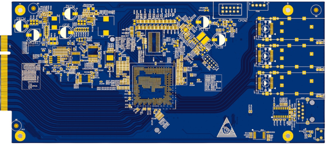
Boards that passed every check at 50 MHz now carry multi-gigabit serial links, memory buses and RF front ends — and the layout habits that worked a decade ago quietly stop working. The phrase high-speed PCB gets used loosely in quotation emails, which is exactly where projects start to go wrong: the buyer assumes the factory understands the constraint, and the factory assumes the buyer knows what to specify.
This article gives you a working definition you can apply to your own design today, the design rules that actually decide yield, the impedance tolerances a production floor can realistically hold, and a pre-production checklist for handing clean data to a manufacturer. No marketing language — just the criteria engineers argue about at engineering review.
Table of Contents
- When a Trace Stops Behaving Like a Wire: High-Speed PCB Criteria
- Impedance Control: What a Factory Can Actually Hold
- Microstrip, Stripline and Coplanar Structures
- Stackup Planning Decides Half the Result
- Choosing Laminate Loss Without Over-Specifying
- Manufacturing Tolerances That Decide Yield
- High-Speed PCB Applications from Backplanes to Optical Modules
- What Actually Moves the Cost of a High-Speed PCB
- A Pre-Production Checklist Before You Release Gerber Data
- FAQ
- Get Your High-Speed PCB Stackup Reviewed Before Production
When a Trace Stops Behaving Like a Wire: High-Speed PCB Criteria
The honest definition is not a data-rate threshold. A trace becomes a transmission line the moment its physical length is a significant fraction of the distance the signal’s edge travels during its rise time. As a working rule of thumb, once a trace is longer than roughly one-sixth of that edge length, reflections, ringing and termination behaviour start to matter — regardless of whether the part is labelled “high speed” in the datasheet.
That is why a 30 MHz SPI bus on a long cable run can behave worse than a short, well-referenced 5 GT/s link. What makes a board a high-speed PCB in practice is the combination of edge rates, trace lengths and impedance sensitivity — not the marketing category of the chipset. If your layout house is already asking about length matching and reference planes, you are there.
| Signal family | Typical data rate | Line impedance | What the layout must hold |
|---|---|---|---|
| PCIe 3.0 / 4.0 | 8–16 GT/s per lane | 85 Ω differential pair | Intra-pair length matching, via stub control |
| USB 3.2 | 5–10 GT/s | 90 Ω differential pair | Pair skew, continuous return path |
| DDR4 memory bus | 2,400 MT/s class | 40–50 Ω single-ended | Fly-by routing, length windows per byte lane |
| HDMI 2.0 | 6 GT/s | 100 Ω differential pair | Intra-pair skew, reference-plane transitions |
| Gigabit Ethernet (SGMII) | 1.25 G/s | 100 Ω differential pair | AC-coupling placement, pair symmetry |
Treat the table as a conversation starter for engineering review rather than a substitute for your own stackup calculation. The values above are the widely used industry targets for each interface class; the final geometry comes out of your dielectric heights and copper weights.
Impedance Control: What a Factory Can Actually Hold
Impedance is the first number to pin down, because every other high-speed decision hangs off it. In volume production the standard tolerance is ±10%. Tighter windows are available, but they move the board into a different process discipline: ±8% is quoted on request with material and etch controls confirmed in advance, and ±5% is handled case by case after engineering review of the stackup.
What buyers often miss is that the factory does not hold tolerance on the bare artwork alone. Etch undercut, copper plating thickness, prepreg thickness variation and solder-mask coverage over outer-layer traces all shift the final impedance. A capable manufacturer models all of these before etching the first panel, then verifies the result on a TDR-measured test coupon that travels with the order.
The practical takeaway for a designer: put your impedance table — net class, target impedance, reference layers — directly into the fabrication drawing. When the table is explicit, the factory can pre-compensate the trace widths for its own process instead of guessing your intent from the artwork.
Microstrip, Stripline and Coplanar Structures
Three transmission-line geometries cover nearly every routing decision on a high-speed PCB. Microstrip runs on an outer layer over a reference plane — fastest, shortest via transitions, but it radiates more and its impedance shifts when solder mask covers it, which is why outer-layer traces get mask compensation. Stripline runs on an inner layer between two planes, giving the best shielding and lowest crosstalk for long critical nets such as memory buses.
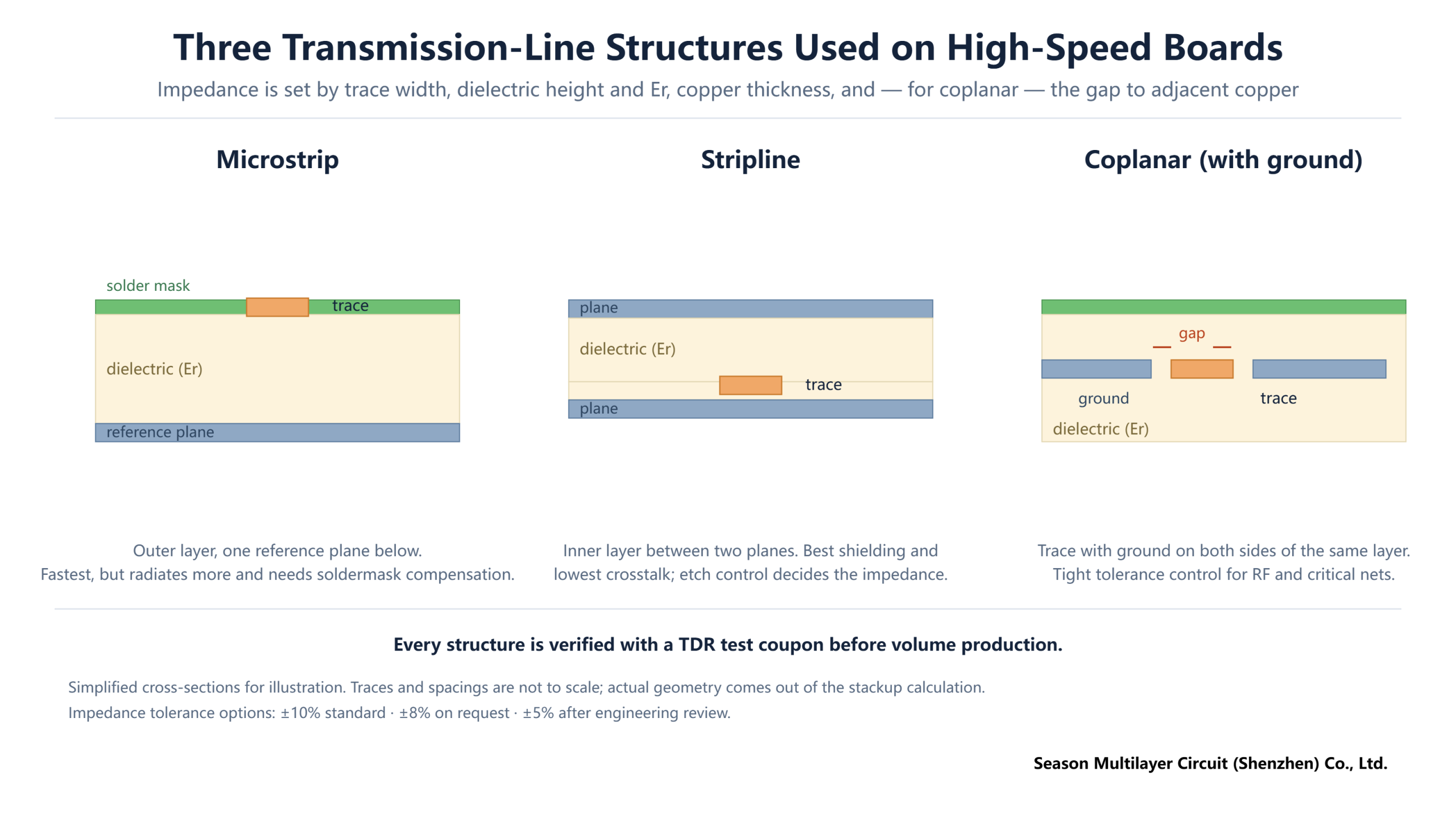
Coplanar structures add ground on both sides of the trace in the same layer, trading a little extra spacing for field containment. They are the default choice at the boundary between digital and RF sections, and anywhere a fixed characteristic impedance must survive process variation. Most mixed-signal boards use all three, so the stackup and the routing rules have to be planned together rather than layer by layer.
Stackup Planning Decides Half the Result
A high-speed stackup is decided by three questions: which reference plane does each signal layer use, how thick is the dielectric between them, and where do the power and ground planes sit. Symmetrical constructions keep the board flat through lamination, but symmetry sometimes conflicts with the impedance targets — those trade-offs are cheap to settle at quotation and expensive to settle after etching.
Keep every fast signal layer adjacent to an unbroken reference plane. A signal crossing a plane split forces the return current to detour, and that detour is where crosstalk and EMI complaints are born. If a layer transition is unavoidable, place a stitching via or a decoupling pair next to the signal via so the return path has somewhere to go.
It is worth reading your manufacturer’s stackup proposal line by line. A competent factory returns a dielectric-by-dielectric table — prepreg style, glass content, copper weights, target impedance per net class — and flags any layer where the target and the process limits disagree before the panel is made. If that document never arrives, the tolerance promise is decorative.
Choosing Laminate Loss Without Over-Specifying
Material selection is where high-speed projects quietly overspend. Loss tangent (Df) and dielectric constant (Dk) set how much signal energy the laminate absorbs and how consistent the impedance stays across the panel — but the right class depends on the length and speed of your longest nets, not on the badge of the interface. A 10 cm DDR4 bus on standard FR-4 can be perfectly sound; a 40 cm 25 GT/s serdes trace usually is not.
The pragmatic sequence is: classify your nets by speed and length, put only the genuinely long or fast ones on a lower-loss material class, and let the rest ride on standard FR-4. Our laminate selection guide walks through that classification, and the material comparison on our PCB materials and laminates page lists the stock grades we cut and laminate daily.
For pure RF and microwave work the material conversation changes character — dielectric constant tolerance and copper foil roughness dominate. That territory is covered separately in our high-frequency PCB material guide, including when a PTFE-based construction is genuinely justified and when a mid-loss material meets the link budget at a fraction of the cost.
Manufacturing Tolerances That Decide Yield
Design files assume ideal geometry; production delivers real geometry. Line-width etch variation, layer-to-layer registration, dielectric thickness tolerance and plating uniformity all consume part of your noise and timing budget. On a design with 3-mil controlled-impedance traces, a 10% etch variation is a visible impedance shift — on 6-mil traces it is background noise. Coarser geometry where you can afford it is the cheapest yield insurance available.
| Parameter | What we run day to day | Notes |
|---|---|---|
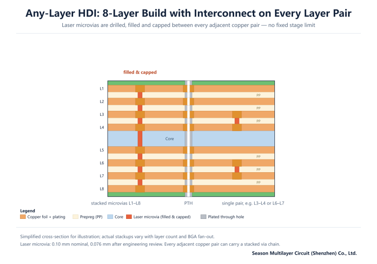
| Layer count | 2–30 layers | Includes 1-N-1 through any-layer HDI builds |
| Min line width / space | 2/2 mil (1.8/1.8 mil on prototypes) | Coarser geometry costs less and yields more |
| Laser microvia | 0.10 mm nominal | 0.076 mm after engineering review |
| Impedance tolerance | ±10% standard, ±8% on request, ±5% on review | Verified by TDR test coupon |
| Surface finish | ENIG, HASL, OSP | Chosen with insertion loss in mind |
The table is a floor, not a ceiling — every line of it is routinely discussed at engineering review, and most of the limits are stretchable on a per-design basis with data in hand. The direction to remember: every tolerance you relax somewhere non-critical buys headroom for the nets that genuinely need it.
High-Speed PCB Applications from Backplanes to Optical Modules
The same physics shows up in very different products. Computing and server boards concentrate the hardest combination: memory buses with strict length windows beside 16 GT/s serdes lanes, all on a 14-layer computing PCB that also has to survive thermal cycling. Networking gear adds backplanes measured in tens of centimetres, where insertion loss and via stubs dominate every stackup meeting.
Automotive and industrial platforms care about the same constraints with a reliability overlay: a 12-layer automotive high-speed backplane spends its life in vibration and temperature swing, so the design rules get stricter and the laminate choice gets more conservative than the raw data rate would suggest. Optical modules invert the problem — tiny boards, extreme speed density — which is exactly what our 6-layer optical module PCB for 100G/400G transceivers is built around.
Consumer devices round out the picture: a flagship phone carries more high-speed interfaces than a small server did a decade ago, squeezed into an HDI construction. The lesson across all of them — the definition of high speed travels with the product, and the manufacturing plan has to be built for the specific mix, not for a category label.
What Actually Moves the Cost of a High-Speed PCB
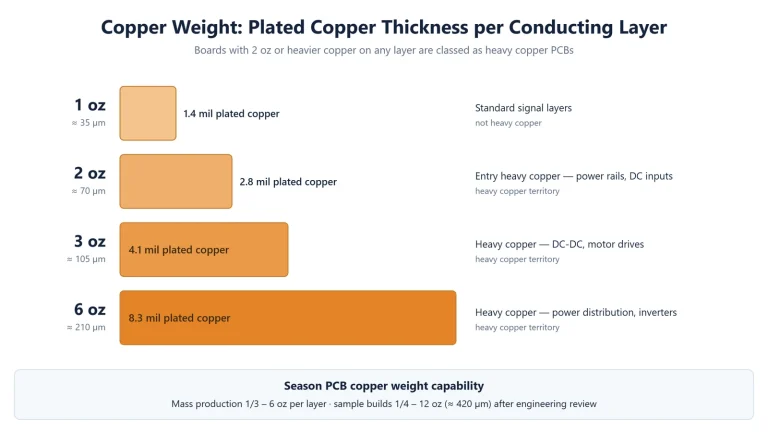
Without a quote in hand, you can still rank the cost drivers with confidence. Layer count leads, because every layer adds material, lamination time and inspection. Laminate class is second — a lower-loss material class typically adds tens of percent to the raw material cost before any other factor. Tight impedance tolerance adds process controls; fine line/space under 3 mil adds yield loss; and every special process (filled microvias, heavy copper, exotic finishes) adds its own multiplier.
The useful habit is to spend only where your nets demand it. Boards that put their entire interconnect on a premium laminate because one bus needed it routinely price two classes above their actual requirement. Bring the net classification to the table early and the cost conversation becomes an engineering decision instead of a negotiation.
A Pre-Production Checklist Before You Release Gerber Data
Most high-speed first-article delays trace back to a handful of missing inputs. Before you send the package, confirm the following — it takes ten minutes and saves a round of engineering-review emails:
- Impedance table: net class, target impedance, reference layer and tolerance for every controlled line
- Stackup request: layer count, total thickness window and any material preference, stated as requirements not suggestions
- Length-matched nets flagged on the fabrication drawing, with the matching window called out
- Return-path notes wherever a critical signal changes reference planes
- Complete, up-to-date Gerber data plus drill files — X2 format with embedded layer attributes removes an entire class of interpretation errors
- Test coupon requirements, if your spec calls for measured impedance evidence with the shipment
If your release process follows IPC documentation practice, the fabrication drawing and the impedance table are the two documents the factory reads first — keep them in sync and the rest of the review is quick. The IPC standards library is the reference point most manufacturers work from.
Frequently Asked Questions
What data rate makes a PCB high speed?
There is no single threshold. A board is high speed when trace lengths are a significant fraction of the signal edge length — long traces with fast edges behave as transmission lines. In practice, designs carrying serdes links above a few GT/s, DDR memory buses, or any net with controlled-impedance requirements qualify.
What impedance tolerance can be held on production boards?
The volume-production standard is ±10%. ±8% is available on request with confirmed material and etch controls, and ±5% is handled case by case after engineering review of the stackup. Every controlled order is verified on a TDR-measured test coupon that accompanies the shipment.
Do I need low-loss laminate for every high-speed design?
No. Material class should follow your longest and fastest nets. Short DDR4 or 5 GT/s links on standard FR-4 are frequently sound; 20 cm-plus multi-gigabit traces usually need a mid- or low-loss class. Classify nets by speed and length first, then pay for loss performance only where the budget requires it.
How is impedance verified before shipment?
Each build panel carries a test coupon that replicates the controlled-impedance structures of your design. The coupon is measured with a TDR probe against the impedance table from your drawing, and the report ships with the boards so incoming inspection can compare numbers directly.
Which files should I send for a high-speed PCB quotation?
Complete Gerber and drill files, the impedance table with reference layers and tolerances, your stackup requirements including total thickness, and any length-matching or coupling notes. The more explicit the fabrication drawing, the fewer assumptions the engineering review has to resolve before pricing.
Can HDI be combined with high-speed design rules?
Yes, and it is common in dense consumer and module designs. Microvias as small as 0.10 mm shorten stub effects compared with through-holes, and filled-and-capped via-in-pad structures free routing channels under BGAs. The stackup review simply has to cover both the impedance plan and the HDI process window together.
How long does a high-speed PCB prototype take?
A typical 8–10 layer controlled-impedance prototype runs in the 17–18 working-day range, with simpler builds faster and complex HDI or low-loss constructions longer. Every timeline is confirmed at engineering review once the actual stackup and process list are known — quoted dates before that review are estimates.
Get Your High-Speed PCB Stackup Reviewed Before Production
Send us your Gerber data, the impedance table and your stackup requirements, and our engineering team will return a dielectric-by-dielectric review — target impedance per net class, process tolerance per layer, and any conflicts between your spec and the manufacturing window — before a panel is made. Start through our PCB manufacturing services page or browse more engineering guides in the PCB basics library.