Book Appointment Now

4-Layer Router PCB
High-performance 4-layer PCBs for network routers — router PCB manufacturing with Gigabit Ethernet, Wi-Fi 6/6E, and multi-port switching. Controlled impedance, EMI shielding, and cost-effective manufacturing for consumer and enterprise networking.
Network routers are the backbone of modern connectivity, requiring PCBs that can handle high-speed Ethernet switching, wireless communication, and processor interfaces with clean signal integrity. At Season PCB, we manufacture 4-layer router PCBs with controlled impedance, EMI shielding, and optimized cost-efficiency for consumer and enterprise networking applications.


4
Layer Count
5/5 mil
Min. Trace/Space
0.20 mm
Min. Via Diameter
Tg 180
Glass Transition Temp
1–2 µ”
ENIG Gold Thickness
ISO 9001:2015
ISO 14001
UL (E305905)
IPC Class 2 / Class 3
RoHS
Table of Contents
4-Layer Router PCB Stackup Diagram
Our 4-layer router PCB stackup is the industry-standard configuration for network router applications, providing dedicated signal routing layers with ground and power plane shielding for Gigabit Ethernet, Wi-Fi, and processor interfaces.
- Top Layer (Copper/Plated): Component placement, Ethernet PHY, Wi-Fi module, SoC
- Inner Layer 2 (Ground Plane): Solid ground reference for top-side signal integrity and EMI shielding
- Inner Layer 3 (Power Plane): Power distribution (3.3V/5V/12V) with decoupling support
- Bottom Layer (Copper/Plated): Bottom routing, Ethernet transformer coupling, test points
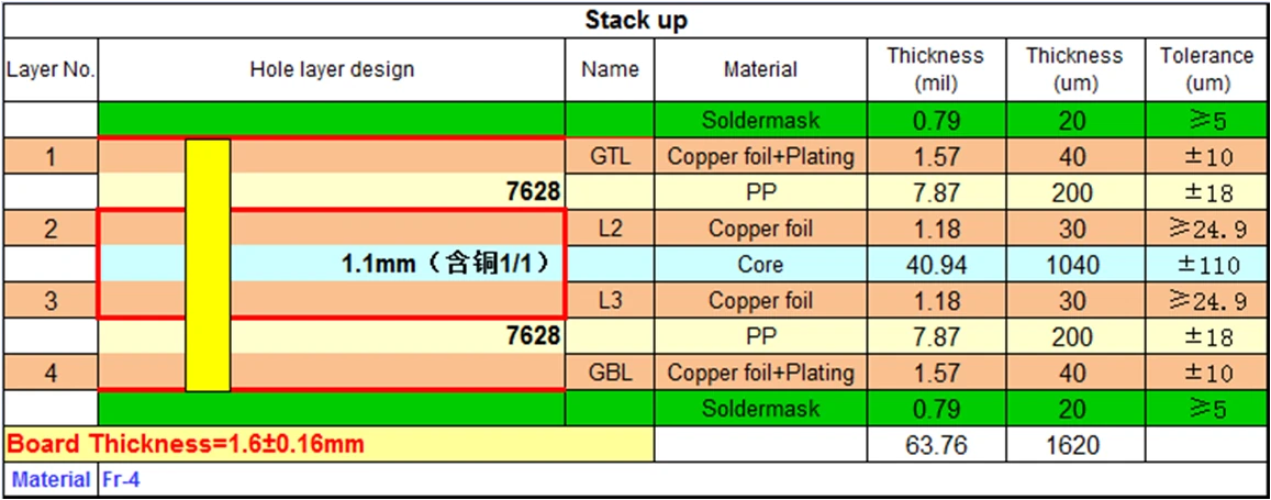
The 4-layer stackup is the optimal balance of performance and cost for router applications. The solid ground plane (L2) provides excellent signal reference for high-speed Ethernet and Wi-Fi traces, while the power plane (L3) ensures clean power distribution. For routers with advanced features like Wi-Fi 6E/7, multi-gigabit Ethernet, or PoE, the 4-layer board may incorporate special features: resin-plugged vias for planar surface under BGA packages, controlled-impedance routing for high-speed Ethernet traces, and thick copper for power delivery.
Impedance control targets for this stackup, per the impedance drawing:

Technical Capability & Specifications
| Parameter | Specification | Advanced Capabilities |
|---|---|---|
| Layer Count | 4 Layer | 2-30L (Mass); 2-64L (Sample) |
| Base Material | FR-4 S1000-2M Tg 180 | SY, NY, TUC, ZY, EMC, KB, ITEQ, Rogers, Megtron, Nelco, Isola |
| Board Thickness | 1.6mm | 0.2-6.4mm (Mass); 0.15-20mm (Sample) |
| Panel Size | 160×120mm | 800×600mm (Mass); 1050×610mm (Sample); custom panelization available |
| Copper Thickness | Outer: 1 oz Inner: 1 oz | Outer: 1/3–12 oz Inner: 1/4–12 oz |
| Min Drill Size | 0.20mm | 0.15mm (Sample) |
| Min Trace Width/Spacing | 5/5 mil | 4/4 mil (Sample) |
| Surface Finish | ENIG | HASL, OSP, Immersion Silver, Immersion Tin, ENIG |
| Solder Mask | Customer-specified color | LPI (liquid photo-imageable), matte or gloss |
| Impedance Control | 50/90/100 OHM | ±5 to ±10 per impedance drawing |
| Controlled Dielectric | Available | Tolerance: ±0.05mm on dielectric thickness |
Key Advantages of Our Router PCB
- Optimized 4-Layer Architecture: Industry-standard signal-ground-power-signal stackup provides excellent signal integrity for Gigabit Ethernet and Wi-Fi applications at the most cost-effective layer count.
- Controlled Impedance for Ethernet: 100 ohm differential impedance control for Gigabit Ethernet pairs ensures reliable high-speed data transmission with minimal bit errors and retransmissions.
- EMI Shielding for Wi-Fi: Solid ground plane (L2) provides effective EMI shielding for Wi-Fi antenna feed lines and RF circuits, preventing interference between wireless and wired network sections.
- Cost-Effective Manufacturing: 4-layer construction with standard materials and processes provides the best price-to-performance ratio for volume router production, enabling competitive product pricing.
- Thermal Management for SoC: 1 oz inner copper power plane acts as a thermal spreader under the router SoC, distributing heat without requiring additional thermal solutions for typical consumer router power levels.
Overcoming Critical Challenges in Router PCB Design
When sourcing PCBs for network router applications, engineers encounter three key challenges. Here is how our engineering team eliminates them:
1. Gigabit Ethernet Signal Integrity
The Problem: Gigabit Ethernet operates at 125 MHz with strict jitter and eye-diagram requirements. Poor PCB layout with improper impedance control, insufficient ground reference, or long stub traces causes signal degradation, packet loss, and reduced throughput.
Our Solution: Our 4-layer stackup routes all Gigabit Ethernet differential pairs on the top layer (L1) with the solid ground plane (L2) as reference. We maintain 100 ohm differential impedance (±10%) through controlled trace geometry and dielectric thickness. Short, direct routes from PHY to magnetics minimize insertion loss and reflections.
2. EMI Interference Between Wi-Fi and Ethernet
The Problem: Routers combine Wi-Fi RF circuits and Gigabit Ethernet on the same board. Without proper isolation, Wi-Fi transmissions couple into Ethernet traces (and vice versa), causing data corruption and regulatory compliance failures.
Our Solution: The solid ground plane (L2) creates a physical shield between the top-side RF/Ethernet section and the bottom-side routing. We recommend physical separation of Wi-Fi and Ethernet sections on the top layer, with grounded copper pour acting as a Faraday shield between them. This achieves >30dB isolation between Wi-Fi and Ethernet circuits.
3. Cost Optimization for Volume Production
The Problem: Consumer routers are price-sensitive products. Over-specifying the PCB (excess layers, premium materials, tight tolerances) increases cost beyond competitive levels. Under-specifying causes performance issues and returns.
Our Solution: Our engineering team works with you to optimize the 4-layer stackup for your specific router design. We identify the minimum required specifications (copper weight, impedance tolerance, material grade) that meet your performance requirements. Standard panel sizes and processes minimize manufacturing cost. The result: optimal price-performance ratio for volume production.
Where Our Router PCBs Are Used
Our 4-layer router PCBs power a wide range of networking applications:
- Home Wi-Fi Routers: Dual-band and tri-band Wi-Fi 6/6E routers with Gigabit Ethernet WAN/LAN ports for residential broadband.
- Mesh Router Nodes: Mesh Wi-Fi system nodes with dedicated backhaul radio and Ethernet backhaul option for whole-home coverage.
- Enterprise Edge Routers: Multi-port enterprise routers with VLAN support, QoS, and VPN capability for SMB networks.
- 4G/5G CPE Routers: Cellular broadband routers combining 4G/5G modems with Wi-Fi and Ethernet for fixed wireless access.
- IoT Gateway Routers: Industrial IoT gateways combining Ethernet, Wi-Fi, Zigbee, and BLE for smart building and factory applications.
Materials and Surface Finish Options for Your Router PCB
Material choice decides how a 4-layer router PCB behaves under 24/7 traffic. Our standard build uses FR-4 S1000-2M (Tg 180), a laminate that holds dielectric thickness and registration through the sustained operating temperatures a router enclosure reaches in a rack or on a shelf. When a design moves to multi-gigabit Ethernet, 2.5G/5G PON, or long board-to-board runs, the same platform extends to lower-loss laminates without changing the four-layer geometry — our PCB laminate selection guide explains how Dk and Df drive that decision.
Surface finish follows the assembly process. ENIG with 1–2 µ” gold is the standard choice because its flat pads keep Ethernet PHY, SoC, and memory packages coplanar across the panel; OSP offers a lower-cost option for lead-free assembly where flatness demands are lighter; electric hard gold suits boards with edge-contact connectors. Our PCB surface finish comparison covers the trade-offs in detail. Prepreg glass style is selected during stackup review so the L1-L2 and L3-L4 dielectrics hit the impedance target with margin — see our prepreg selection rules.
In a typical build, those choices land as follows:
- FR-4 S1000-2M (Tg 180) standard; low-loss laminates for multi-gigabit designs
- ENIG 1–2 µ” standard; OSP for cost-optimized builds; hard gold for edge contacts
- Prepreg glass style chosen in stackup review to hold impedance margin
- Halogen-free laminates available for eco-certified router programs
Inside Our 4-Layer Router PCB Production Process
Every 4-layer router PCB order starts with a DFM review focused on what four-layer geometry punishes: impedance reference continuity for the Gigabit Ethernet pairs, copper balance across the 1.1mm core, PoE current paths on the L3 power plane, and BGA fanout against the 0.2mm minimum drill. Corrections at this stage cost a file edit; the same issues found after lamination cost a production run.
On the line, the inner layers are imaged, etched, and AOI-inspected before lamination bonds them around the core with 7628 prepreg. X-ray alignment holds layer-to-layer registration through pressing, and the finished board thickness is verified against the 1.6mm nominal before drilling. Through-hole vias are drilled, copper-plated, and capped by the outer-layer imaging, plating, and etch sequence, then solder mask and surface finish are applied and the panel is routed to size.
Verification closes the loop: finished panels go through 100% electrical testing before packing, and impedance coupons travel with every production panel — measured by TDR against your 50/100 ohm targets, with a report shipped in each batch. Our PCB impedance measurement guide explains how TDR and VNA methods verify those numbers.
Our Quality Guarantee for Router PCBs
Network router electronics require consistent signal quality and reliability. We implement rigorous testing protocols on every board:
- 100% AOI Inspection: every layer scanned for trace breaks, shorts, and registration drift against the Gerber master.
- 100% Electrical Testing (E-Test): flying probe or fixture testing confirms continuity and isolation on the finished panel, checked against your CAD netlist.
- Controlled Impedance Testing: TDR measurement on coupons from every panel, reported against your 50/100 ohm Ethernet and RF targets on a Polar Instruments report.
- Solder Mask Inspection: Visual and automated inspection of solder mask coverage on impedance-controlled traces.
- Certifications: ISO 9001:2015, ISO 14001, UL (E305905), RoHS compliant. IPC Class 2 standard, Class 3 available.
Why Choose Season PCB for Your Router PCB?
With 20 years of experience in PCB manufacturing, Season PCB has served over 8,000 global clients in networking, consumer electronics, and telecommunications. Our three manufacturing facilities provide capacity for both rapid prototyping and high-volume production.
We understand that router PCBs require a balance of signal integrity, EMI shielding, and cost efficiency. That is why every 4-layer router PCB we ship is backed by:
- Free DFM file checking before production
- 24/7 dedicated engineering support
- Delivery scheduling aligned with your program milestones
- Prototype-to-production flexibility — from a single build to full-volume programs
- Engineering fee waivers on bulk production orders
Season PCB builds 4-layer router PCB boards for Wi-Fi routers, mesh systems, and enterprise networking — controlled impedance for Gigabit Ethernet, EMI shielding for Wi-Fi coexistence, and a stackup that stays inside consumer price targets.
Send us your layer count, target impedance, and annual volume, and our engineers will reply with a DFM-checked quote and a stackup recommendation.
Every build complies with UL safety certifications and IPC manufacturing standards. For volume production, the same stackup runs on 998PCB Group’s high-speed and high-frequency PCB lines at the group’s Shenzhen campus.
Frequently Asked Questions
Is 4 layers enough for Wi-Fi 6E routers?
For most consumer Wi-Fi 6E routers, 4 layers is sufficient. The solid ground plane (L2) provides adequate EMI shielding for Wi-Fi 6E (6 GHz band) and Gigabit Ethernet signals. However, for routers with Wi-Fi 7 (320 MHz channels, 4K-QAM), multi-gigabit Ethernet (2.5G/10G), or complex PoE, we recommend upgrading to 6 layers for additional signal routing and isolation.
What impedance tolerance do you offer for Gigabit Ethernet?
Standard impedance control tolerance is ±10% for 100 ohm differential pairs on 4-layer boards. For critical Gigabit Ethernet applications, we can achieve ±8% with tighter control on trace geometry and dielectric thickness. Every batch includes a Polar Instruments impedance test report.
What is the typical lead time for 4-layer router PCB prototypes?
Prototype and mass-production schedules for your router PCB are confirmed with your quotation and depend on stackup complexity and order volume. Fast-turn options are available and quoted upfront so you can plan development milestones with certainty.
What materials and surface finishes are available for the 4-layer router PCB?
The standard build is FR-4 S1000-2M (Tg 180), with SY, NY, TUC, ZY, EMC, KB, ITEQ, Rogers, Megtron, Nelco, and Isola laminates available on request. Board thickness is 1.6mm standard (0.2-6.4mm for mass production, 0.15-20mm for samples) with 1 oz copper on outer and inner layers, expandable up to 12 oz. ENIG is the standard surface finish, with HASL, OSP, immersion silver, and immersion tin optional. Solder mask color is customer-specified, in LPI with matte or gloss finish.
How do you verify quality on 4-layer router PCBs?
Three checks gate every shipment: inner-layer AOI before lamination, 100% electrical test on the finished panel, and TDR measurement on impedance coupons that travel with the batch. The Polar Instruments report ships with each order, so it can be filed directly with your incoming inspection records. Our quality system is certified to ISO 9001:2015 and ISO 14001, listed to UL (E305905), and RoHS compliant, with IPC Class 2 and Class 3 builds both available.
Ready to start your Router PCB project?
Whether your program calls for early prototype builds or full-volume production, our engineering team is ready to support your router project with DFM review, impedance modeling, and fast-turn fabrication.
Tel: (+86) 18681528532 | WhatsApp: +86 18681528532
E-mail: roc@season-pcb.com