Book Appointment Now

10-Layer HDI Industrial Control PCB
High-reliability 10-layer HDI PCBs for industrial control systems — industrial control PCB manufacturing with multi-protocol communication, real-time processing, and rugged reliability for factory automation, PLCs, and motion control in harsh industrial environments.
Industrial control systems demand PCBs that can handle high-speed processing, multiple communication protocols, and harsh environmental conditions — all while maintaining 24/7 reliability. From PLCs to motion controllers, the PCB is the critical backbone of industrial automation. At Season PCB, we manufacture 10-layer HDI industrial control PCBs with blind/buried vias, robust EMI shielding, and industrial-grade thermal management.


1+8+1
Layer Count
3/3 mil
Min. Trace/Space
0.10mm
Min. Via Diameter
Tg 180
Glass Transition Temp
1–2 µ”
ENIG Gold Thickness
ISO 9001:2015
ISO 14001
UL (E305905)
IPC Class 2 / Class 3
RoHS
IATF16949
Table of Contents
10-Layer HDI Industrial Control PCB Stackup Diagram
Our standard 10-layer HDI industrial control PCB stackup is a 1.6 +/-0.16 mm 1+8+1 build on FR-4 S1000-2M (Tg 180): three 0.152 mm cores carry the L3–L4, L5–L6 and L7–L8 buried via pairs, 1080 prepreg bonds every layer, and 0.10mm laser blind vias tie the outer component layers to the system. That gives complex multi-processor controllers comprehensive EMI shielding, multiple power domains and high-density routing in one board. The table below lists the material, thickness and tolerance of every layer, followed by the impedance targets we hold on the released build.
| Layer | Material | Thickness | Function / Design Note |
|---|---|---|---|
| Solder mask | — | 20 µm (≥5) | Applied top and bottom |
| L1 (Top) | Copper foil + plating (GTL) | 35 µm ±10 | CPU/FPGA, communication ICs, I/O connectors; 50 ohm single-ended and 85/90/100 ohm differential to L2 |
| Prepreg | 1080 | 72 µm ±13 | L1–L2 blind-via dielectric |
| L2 | Copper foil + plating | 30 µm (≥24.9) | EMI shielding plane for top-side signals; 40/50 ohm single-ended and 80 ohm differential to L1/L3 |
| Prepreg | 1080 ×2 | 149 µm ±18 | L2–L3 dielectric |
| L3 | Copper foil + plating | 30 µm (≥24.9) | High-speed data bus routing (PCIe, EtherCAT) |
| Core | FR-4, 0.152 mm (no copper) | 152 µm ±18 | Core 1; buried vias connect L3 to L4 |
| L4 | Copper foil | 30 µm (≥24.9) | Core voltage distribution (3.3V/1.2V) |
| Prepreg | 1080 ×2 | 147 µm ±18 | L4–L5 dielectric |
| L5 | Copper foil | 30 µm (≥24.9) | Signal reference plane; buried vias connect L5 to L6 |
| Core | FR-4, 0.152 mm (no copper) | 152 µm ±18 | Core 2 |
| L6 | Copper foil | 30 µm (≥24.9) | Communication protocol routing (CAN, RS-485) |
| Prepreg | 1080 ×2 | 148 µm ±18 | L6–L7 dielectric |
| L7 | Copper foil | 30 µm (≥24.9) | I/O power distribution (24V/5V); buried vias connect L7 to L8 |
| Core | FR-4, 0.152 mm (no copper) | 152 µm ±18 | Core 3 |
| L8 | Copper foil | 30 µm (≥24.9) | Analog sensor routing; 40/50 ohm single-ended and 80/90/100 ohm differential to L7/L9 |
| Prepreg | 1080 ×2 | 148 µm ±18 | L8–L9 dielectric |
| L9 | Copper foil + plating | 30 µm (≥24.9) | Bottom-side signal reference plane |
| Prepreg | 1080 | 72 µm ±13 | L9–L10 blind-via dielectric |
| L10 (Bottom) | Copper foil + plating (GBL) | 35 µm ±10 | Bottom routing and thermal dissipation; 50 ohm single-ended and 85/90/100 ohm differential to L9 |
| Solder mask | — | 20 µm (≥5) | Applied top and bottom |
| Finished board | FR-4 S1000-2M, Tg 180 | 1.6 +/-0.16 mm finished (1,544 µm layer sum) | 1+8+1 build: blind vias L1–L2 / L9–L10, buried vias L3–L4 / L5–L6 / L7–L8 |
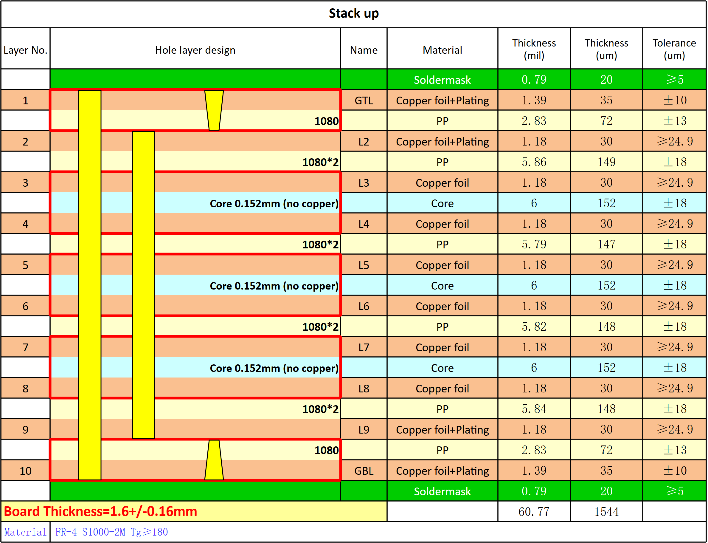
The 10-layer architecture provides three dedicated ground planes (L2, L5, L9) and two power planes (L4, L7), creating exceptional EMI shielding for noisy industrial environments. If your design requires adjustments, our engineering team will optimize the stackup for your specific application.
Need more routing headroom than this 1+8+1 build offers? Our 14-layer 2-stage HDI prototype PCB scales the same stacked-microvia approach to a 2+10+2 build-up with 2.5/2.5 mil lines and a central L7/L8 power-ground pair.
Impedance and Design Rules on This Stackup
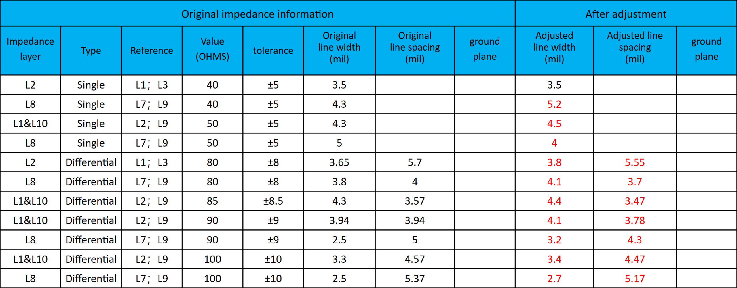
- Hold the released impedance table. Single-ended traces run at 40/50 ohm with a +/-5% tolerance and differential pairs at 80/85/90/100 ohm with +/-8–10%; every adjusted line width and spacing in the table above is the release value we etch to.
- Keep references on both faces. Each impedance layer is quoted with references on both sides — L2 to L1/L3, L8 to L7/L9, and the outer layers to L2/L9 — so return paths never detour across a split plane. See how we verify each value in our PCB impedance measurement guide.
- Put the layer jumps in the cores. Three 0.152 mm cores carry the L3–L4, L5–L6 and L7–L8 mechanical buried vias, keeping dense interlayer jumps off the crowded outer layers.
- Use blind vias only at the surface. 0.10mm laser blind vias connect L1 to L2 and L9 to L10, tying fine-pitch components to the inner system without stacked-microvia risk. Our blind and buried via HDI guide covers how these structures are built and costed.
- Size the board for the enclosure. The finished 1.6 +/-0.16 mm thickness gives DIN-rail and cabinet-mounted controllers the rigidity for card guides, locking connectors and vibration. For a lighter build, our 6-layer industrial control PCB guide compares the 6-layer stackup.
Technical Capability & Specifications
| Parameter | Specification | Advanced Capabilities |
|---|---|---|
| Layer Count | 10 Layer HDI | 2-30L (Mass); 2-64L (Sample) |
| Base Material | FR-4 S1000-2M Tg 180 | SY, NY, TUC, ZY, EMC, KB, ITEQ, Rogers, Megtron, Nelco, Isola |
| Board Thickness | 1.6mm | 0.2-6.4mm (Mass); 0.15-20mm (Sample) |
| Panel Size | 160 x 120 mm (1-up) | 800x600mm (Mass); 1050x610mm (Sample) |
| Copper Thickness | Outer: 1 oz (35 µm plated) Inner: 0.75 oz (30 µm foil) | Outer: 1/3–12 oz Inner: 1/4–12 oz |
| Min Drill Size | 0.10mm (Laser) | 0.075mm (Laser Sample) |
| Min Trace Width/Spacing | 3/3 mil | 2.5/2.5 mil (Sample) |
| Blind Via | 0.10mm Laser | 0.075mm Laser (Sample) |
| Buried Via | 0.15mm Mechanical | 0.127mm (Sample) |
| Surface Finish | ENIG | HASL, OSP, Immersion Silver, Immersion Tin, ENIG, ENEPIG |
| Solder Mask | Customer-specified color | LPI (liquid photo-imageable), matte or gloss |
| Impedance Control | Single-ended 40/50 Ohm ±5% Differential 80/85/90/100 Ohm ±8–10% | Custom impedance targets on request |
Key Advantages of Our Industrial Control PCB
- Triple Ground Plane Shielding: Three dedicated ground planes (L2, L5, L9) provide comprehensive EMI shielding for high-speed data buses, critical in industrial environments with heavy electromagnetic interference.
- Multi-Domain Power Distribution: Separate power planes for core voltage (L4) and I/O power (L7) prevent power supply noise from coupling between sensitive processing circuits and noisy I/O drivers.
- HDI Density for Complex Processing: Blind and buried vias enable high-density routing for multi-core processors, FPGAs, and communication ICs within standard industrial form factors.
- Industrial-Grade Reliability: High-TG FR4 (Tg 180) with 1.6mm board thickness provides mechanical rigidity and thermal stability for harsh industrial environments with vibration and temperature cycling.
- Multi-Protocol Support: Dedicated signal layers for high-speed buses (PCIe, EtherCAT) and industrial communication protocols (CAN, RS-485, PROFIBUS) with proper impedance control.
Overcoming Critical Challenges in Industrial Control Design
When sourcing HDI industrial control PCBs, engineers encounter three critical challenges. Here is how our engineering team eliminates them:
1. EMI-Induced Communication Errors
The Problem: Industrial environments are electrically noisy with motors, VFDs, and welders generating EMI. Poor PCB shielding causes communication errors on CAN, RS-485, and EtherCAT buses, leading to process interruptions and safety risks.
Our Solution: Our 10-layer stackup uses three ground planes (L2, L5, L9) to create Faraday cage-like shielding around every signal layer. High-speed communication buses are routed on inner layers with solid ground references above and below for effective EMI rejection. The result: error-free communication in the harshest industrial environments.
2. Thermal Management for High-Power Processors
The Problem: Industrial controllers use powerful CPUs and FPGAs that generate significant heat. Without proper thermal management, junction temperatures exceed safe limits, causing thermal throttling, erratic behavior, and premature failure.
Our Solution: We optimize thermal via arrays under hot components, connecting them to the bottom copper layer through dedicated thermal channels. The multiple ground planes act as thermal spreaders, distributing heat across the board. For extreme thermal loads, we offer heavy copper pours (up to 12 oz) on standard FR-4 builds.
3. Signal Integrity for Mixed-Voltage Systems
The Problem: Industrial controllers combine 24V I/O, 5V logic, 3.3V peripherals, and 1.2V core voltages on one board. Without proper power plane isolation, voltage transients from I/O switching couple into sensitive processing circuits, causing resets and data corruption.
Our Solution: The 10-layer stackup dedicates separate power planes for core voltage (L4) and I/O power (L7), with ground planes between them for isolation. This star-topology power distribution prevents transient coupling between voltage domains, ensuring stable processor operation even during heavy I/O switching.
Where Our Industrial Control PCBs Are Used
Our 10-layer HDI industrial control PCBs power a wide range of industrial automation applications:
- Programmable Logic Controllers (PLC): Multi-processor PLC boards with digital/analog I/O, communication modules, and real-time control logic.
- Motion Control Systems: Multi-axis servo and stepper motor controllers with EtherCAT communication and FPGA-based trajectory planning.
- Industrial PCs (IPC): Rugged industrial computer motherboards with PCIe expansion, multiple Ethernet ports, and industrial I/O.
- SCADA Communication Gateways: Protocol conversion gateways connecting field devices (Modbus, PROFIBUS) to upper-level networks (EtherCAT, Profinet).
- Human-Machine Interface (HMI) Controllers: Touch panel controllers with high-speed display interfaces and industrial communication ports.
Our Quality Guarantee for Industrial Control PCBs
Industrial control electronics operate 24/7 and cannot tolerate failures. We implement rigorous testing protocols on every industrial control PCB:
- 100% AOI Inspection: Automated Optical Inspection scans every layer for trace breaks, shorts, and alignment errors.
- 100% Electrical Testing (E-Test): Flying probe or fixture-based testing verifies continuity and isolation on every board.
- Controlled Impedance Testing: Polar Instruments test report documenting compliance with specified impedance values.
- Thermal Stress Testing: Available thermal cycling testing per IPC-TM-650 for harsh environment qualification.
- Certifications: ISO 9001:2015, ISO 14001, UL (E305905), RoHS compliant. IPC Class 3 available for critical applications.
Why Choose Season PCB for Your Industrial Control PCB?
Since 2006, Season PCB has served global clients in industrial automation, process control, and telecommunications. Our three manufacturing facilities provide capacity for both rapid prototyping and high-volume production.
We understand that industrial control electronics demand zero-failure reliability in harsh environments. That is why every 10-layer HDI industrial control PCB we ship is backed by:
- Free DFM file checking before production.
- 24/7 dedicated engineering support.
- Proactive production status updates at every build stage.
- Flexible order volumes — from 1 prototype to 100,000+ units.
- Engineering fee waivers on bulk production orders.
Season PCB specializes in 10-layer HDI industrial control PCB manufacturing for factory automation and process control applications. Our industrial control PCB products feature triple ground plane EMI shielding, multi-domain power distribution, and industrial-grade reliability. Each industrial control PCB meets IPC standards.
For your industrial control PCB needs, Season PCB provides fast turnaround, competitive pricing, and ISO-certified quality. Contact us for industrial control PCB manufacturing today.
Our industrial control PCB boards comply with UL safety certifications and IPC manufacturing standards. Each industrial control PCB undergoes thermal stress testing and signal integrity verification. The same build scales to high volumes on 998PCB Group’s advanced HDI PCB lines at the group’s Shenzhen campus.
If your industrial controller needs denser BGA fan-out than this 1+8+1 build provides, our 10-layer 2-stage HDI prototype PCB adds stacked microvia-in-pad and 0.2 mm BGA via-in-pad capability on a simplified 2+6+2 stackup.
Frequently Asked Questions
Why use 10 layers for industrial control PCBs?
Industrial controllers integrate multi-core processors, FPGAs, multiple communication protocols, and mixed-voltage I/O on one board. 10 layers provide dedicated ground planes for EMI shielding, separate power planes for voltage isolation, and sufficient signal layers for high-density routing — all critical for reliable industrial operation.
Can you support IPC Class 3 manufacturing for industrial PCBs?
Yes, we offer IPC Class 3 manufacturing for critical industrial applications. This includes tighter annular ring requirements, enhanced plating quality, and 100% visual inspection per IPC-A-600 Class 3 criteria. Additional lead time may apply for Class 3 qualification.
What impedance tolerances do you offer for industrial communication buses?
Single-ended impedances run at 40 and 50 ohm with a +/-5% tolerance, and differential impedances cover 80, 85, 90, and 100 ohm at +/-8 to +/-10%, as released in the impedance design table. Tighter targets can be engineered on request. Every batch includes a Polar Instruments impedance test report.
What materials and surface finishes are available for 10-layer HDI industrial control PCBs?
The standard build is FR-4 S1000-2M (Tg 180) at 1.6mm board thickness, with SY, NY, TUC, ZY, EMC, KB, ITEQ, Rogers, Megtron, Nelco, and Isola laminates available on request. Our 1+8+1 industrial control PCB stackup uses 0.10mm laser blind vias and 0.15mm mechanically drilled buried vias, with minimum laser drill down to 0.075mm and 3/3 mil trace width and spacing (2.5/2.5 mil on samples). Copper is 1 oz outer (35 µm plated) and 0.75 oz inner (30 µm foil), expandable up to 12 oz.
ENIG is the standard surface finish, with HASL, OSP, immersion silver, immersion tin, and ENEPIG optional. Solder mask color is customer-specified, in LPI with matte or gloss finish. Controlled impedance covers single-ended 40 and 50 ohm at plus/minus 5% and differential 80, 85, 90, and 100 ohm at plus/minus 8 to 10%.
How do you verify quality on industrial control PCBs?
Every board passes 100% AOI, which scans every layer for trace breaks, shorts, and alignment errors, plus 100% electrical testing by flying probe or fixture to verify continuity and isolation. A Polar Instruments impedance test report documents compliance with the specified impedance values for each batch, and thermal stress testing per IPC-TM-650 is available for harsh-environment qualification. We are certified to ISO 9001:2015, ISO 14001, UL (E305905), and RoHS, with IPC Class 3 manufacturing available for critical applications.
Ready to start your Industrial Control PCB project?
Whether you need 5 pieces for prototyping or 50,000 for mass production, our engineering team is ready to support your industrial control PCB project with DFM review, impedance modeling, and fast-turn fabrication.
Tel: (+86) 18681528532 | WhatsApp: +86 18681528532
E-mail: roc@season-pcb.com