Book Appointment Now

Fast PCB Manufacturing: 8-Layer Computer Peripheral Boards
Premium multilayer PCBs engineered for high-speed computer peripherals. Your fast PCB partner for rapid turnaround, precision impedance control, and zero-compromise signal integrity.
When your product launch deadline is measured in days, not weeks, you need a fast PCB partner who can deliver. At Season Multilayer Circuit, we manufacture fast PCBs — specifically 8-layer computer peripheral boards with rapid prototype delivery, precision impedance control, and industrial-grade reliability. Whether you are building gaming controllers, Thunderbolt docks, video capture cards, or Hi-Fi audio interfaces, our boards deliver the signal integrity and power stability your devices demand.


8
Layer Count
3/3 mil
Min. Trace / Space
0.20 mm
Min. Via Diameter
Tg 180
Glass Transition Temp
1-2 µ”
ENIG Gold Thickness
ISO 9001:2015
ISO 14001
UL (E305905)
IPC Class 2 / Class 3
IATF 16949
RoHS
Table of Contents
- Overview
- Stackup Diagram
- Technical Specifications
- Key Advantages
- Design Challenges
- Challenge 1: Signal Integrity
- Challenge 2: Thermal Management
- Challenge 3: Power Delivery
- Applications
- Materials and Finishes
- Production Process
- Design Guidelines
- File Prep and Panelization
- Quality Guarantee
- Why Choose Season PCB
- FAQ
8-Layer Computer Peripheral PCB Stackup Diagram
For high-speed computer peripherals, signal integrity is critical. Our standard 8-layer stackup maximizes shielding by sandwiching high-speed routing layers between solid ground and power planes, drastically minimizing cross-talk and ensuring clean signal transmission for USB 3.2, PCIe, and HDMI interfaces.
- Top Layer (Copper / Plated): Component Placement & High-Speed Signal Routing
- Inner Layer 2 (Ground Plane): Reference Shielding for L1 & L3
- Inner Layer 3 (Signal Layer): Controlled Impedance (Differential Pairs)
- Inner Layer 4 (Power Plane): Dedicated Power Distribution
- Inner Layer 5 (Ground Plane): Shielding Between Signal Layers
- Inner Layer 6 (Signal Layer): Controlled Impedance (Single-Ended)
- Inner Layer 7 (Ground Plane): Reference Shielding for L6 & L8
- Bot Layer (Copper / Plated): Secondary Routing & Thermal Dissipation
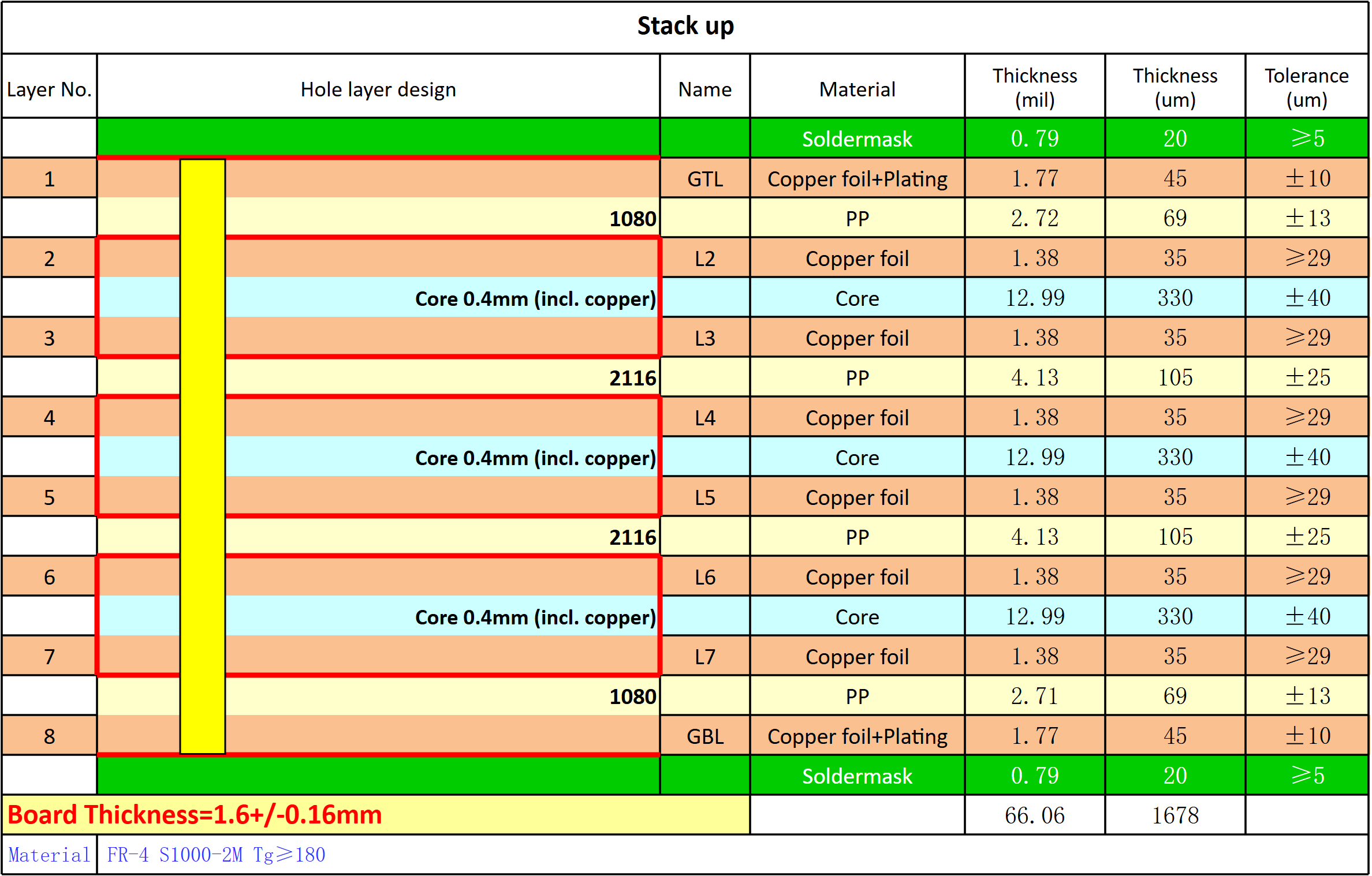
If your current trace widths and spacings fall outside strict impedance tolerance zones, there is no need to worry. Our engineering team will design the optimal stackup architecture for your specific layout, making micro-adjustments to your original trace dimensions to guarantee your board performs exactly as intended.

Technical Capability & Specifications
| Parameter | Specification | Advanced Capabilities |
|---|---|---|
| Layer Count | 8 Layer | 2-30L (Mass); 2-64L (Sample) |
| Base Material | FR-4 S1000-2M Tg 180 | SY, NY, TUC, ZY, EMC, KB, ITEQ, Rogers, Megtron, Nelco, Isola |
| Board Thickness | 1.6mm | 0.2-6.4mm (Mass); 0.15-20mm (Sample) |
| Panel Size | 145*119mm | 800*600mm (Mass); 1050*610 (Sample) |
| Copper Thickness | Outer: 1 oz Inner: 1 oz | Outer: 1/3–12 oz Inner: 1/4–12 oz |
| Min Drill Size | 0.2mm | 0.15mm (Mass); 0.127mm (Sample) |
| Min Trace Width/Spacing | 3/3 mil | 2.5/2.5 mil (Mass); 2/2 mil (Sample) |
| Min Annular Ring | 4 mil | 3 mil (Mass); 2 mil (Sample) |
| Surface Finish | ENIG | HASL, OSP, Immersion Silver, Immersion Tin, ENEPIG |
| Solder Mask | Customer-specified color | LPI (liquid photo-imageable), matte or gloss |
| Impedance Control | 50/85/90/100Ω ±8% | ±5% available for ultra-high-speed |
Key Advantages of Our Fast PCB Manufacturing Service
- Streamlined Fast PCB Turnaround: Dedicated quick-turn production lines and three manufacturing facilities keep every program moving. We understand that time-to-market is critical — that is why our fast PCB service prioritizes speed without sacrificing quality.
- Precision Impedance Control: Strict ±8% tolerance (50Ω/85Ω/90Ω/100Ω) for high-speed USB 3.2, PCIe Gen 3/4, and HDMI 2.1 signal integrity, with ±5% available for ultra-high-speed applications.
- High-TG FR4 Materials: Built with Tg ≥180°C materials to withstand demanding thermal environments in computer peripherals and gaming hardware.
- Prototype to Production: Start with a single prototype and scale smoothly into mass production as your program grows.
- Free DFM Review: Every design is reviewed by our engineering team before production. We catch design issues before they become manufacturing defects.
Overcoming Critical Challenges in Peripheral Hardware Design
When sourcing multilayer boards for computer peripheral applications, electronic buyers and engineers routinely encounter three major failure points. Here is how our engineering team eliminates them:
1. Signal Integrity in High-Speed Digital Interfaces
The Problem: Low-quality stackups cause electromagnetic interference (EMI), leading to packet loss, data corruption, and signal degradation in high-speed USB 3.2, PCIe, and HDMI interfaces. When a gaming controller lags or a video capture card drops frames, the entire user experience is compromised.
Our Solution: Our 8-layer fast PCB architecture uses tightly coupled interleaved ground planes (L2, L5, L7) to block cross-talk and maintain clean high-speed digital signals. Every signal layer is adjacent to a solid ground reference, ensuring clean return paths and minimal EMI radiation. The result: stable, lag-free performance for gaming peripherals, video capture, and Thunderbolt docks.
2. Thermal Management in Compact Enclosures
The Problem: Compact computer peripherals like gaming controllers, USB-C docks, and streaming encoders pack high-power components into unventilated enclosures, causing rapid thermal buildup. Internal temperatures can exceed 85°C, leading to capacitor bulging, IC failure, and premature device death.
Our Solution: Our fast PCB manufacturing uses premium High-TG materials (Tg ≥180°C) paired with optimized thermal via arrays to pull heat away from critical ICs. The central ground plane (L5) acts as a thermal spreader, distributing heat evenly across the board. For extreme environments, we offer heavy copper pours and metal-core PCB options for maximum thermal dissipation.
3. Power Delivery Instability in Multi-Function Peripherals
The Problem: Multi-function USB-C docks and Thunderbolt peripherals demand heavy power delivery — up to 100W for charging, video, and data simultaneously. Substandard fast PCBs overheat or suffer massive voltage drops when delivering this much power, causing connected devices to brown out or reset.
Our Solution: We optimize your fast PCB trace widths for the power budget and offer heavy inner copper options (up to 12 oz) to handle high-wattage USB-C Power Delivery safely without thermal buildup. Our PCB manufacturing services include full DFM review of your power distribution network to ensure stable voltage at the load.
Applications for Our Fast PCB Solutions
Our fast PCB solutions power a wide range of computer peripheral and consumer electronics applications:
- Gaming Peripherals: High-performance gaming mice, mechanical keyboards, and controllers requiring ultra-low latency signal transmission and precise impedance control for responsive gameplay.
- Video Capture & Streaming: USB 3.2 capture cards, HDMI splitters, and streaming encoders that demand clean high-speed data paths and reliable thermal management.
- Thunderbolt & USB-C Docks: Multi-function docking stations with power delivery, video output, and data transfer. Heavy copper power planes ensure stable 100W delivery.
- Hi-Fi Audio Interfaces: Professional USB audio interfaces and DACs requiring ultra-low-noise signal paths and clean power separation between analog and digital domains.
- Wireless Connectivity Modules: Wi-Fi 6/6E and Bluetooth 5.3 adapter boards with precise RF impedance control and EMI shielding for stable wireless performance.
- Smart Computing Peripherals: AI-accelerated compute sticks, NPU modules, and edge computing devices that require dense, high-layer-count boards with superior thermal management.
Materials and Surface Finish Options
Every fast PCB build starts with the right material. Our standard 8-layer construction uses FR-4 S1000-2M with Tg ≥180°C, a high-reliability laminate that withstands demanding thermal environments. For designs that push signal boundaries further, we also support high-speed and low-loss laminate systems from leading material suppliers, including Rogers, PTFE-based laminates, and Megtron and Nelco series for ultra-low-loss stackups.
Surface finish has a direct impact on solderability, contact durability, and long-term reliability. ENIG is the standard finish for this fast PCB platform, providing a flat, coplanar surface for fine-pitch components. Depending on your assembly process, we also offer HASL, OSP, immersion silver, immersion tin, and ENEPIG. Each option is documented in your DFM report so you can confirm the best match for your assembly line before production begins.
Solder mask protection uses LPI application in matte or gloss, giving your fast PCB a durable finish that withstands multiple reflow cycles. Silkscreen legend is printed to your artwork, keeping assembly references clear for your production line.
- FR-4 S1000-2M Tg ≥170°C standard; low-loss and high-speed laminates available for advanced designs
- ENIG standard finish; HASL, OSP, immersion silver, immersion tin, and ENEPIG options
- 1 oz copper as standard, with heavier copper available for power-dense layouts
- UL-recognized laminate systems and RoHS-compliant processing throughout
Inside Our Fast PCB Production Process
Speed on this scale does not come from cutting corners — it comes from a disciplined, tightly integrated process. When your Gerber files arrive, our engineering team runs a full DFM review covering stackup, impedance targets, drill files, and panelization. Questions are resolved by our engineers before tooling begins, so the design moves through production without avoidable stops.
On the floor, your fast PCB travels a carefully balanced line: CNC drilling with dedicated drill sets for 0.2 mm minimum vias, automated copper plating, LDI imaging for precise trace definition down to 3/3 mil, and lamination in multi-zone vacuum presses that keep the 1.6 mm build flat and stable. Every inner layer passes AOI before lamination, so defects are caught while they are still easy to correct.
After final fabrication, each panel goes through 100% electrical testing, with flying-probe verification supporting impedance coupons analyzed on Polar Instruments systems. A dedicated inspection report documents the results for your batch, giving your assembly team full traceability from laminate lot to shipped board.
Between process steps, MES tracking records every panel position, drill set, and test result. If a question ever arises about a delivered board, we can trace its full history from laminate lot to shipment — a level of traceability that normally requires dedicated quality staff at your end.
Design Guidelines for a Smooth Fast PCB Build
A few early design decisions make the difference between a smooth fast PCB build and a stalled one. Start impedance planning at layout kick-off, not at CAM review: define your 50/85/90/100Ω targets, the layers they reference, and the tolerance you need. Keep the stackup symmetric — our standard 8-layer build balances signal, ground, and power layers — and route high-speed pairs with solid reference planes to hold impedance through the full ±8% window.
- Route controlled-impedance pairs over unbroken ground planes — L2, L5, and L7 in the standard build
- Design with 3/3 mil minimum trace and space, 4 mil annular rings, and 0.2 mm minimum drills in mind
- Use thermal via arrays near hot components to spread heat into inner copper
- Panelize around our standard 145*119 mm working panel for efficient material use
If any of these guidelines collide with your layout, send the design anyway. Our DFM engineers review every fast PCB file individually and propose the smallest workable adjustment — a shifted trace, a resized via, or a rebalanced stackup — so your board performs exactly as intended.
To verify impedance before committing to a production batch, we can build a first-article panel with impedance coupons on your stackup. Measurements are taken on Polar Instruments systems and reported with the batch, so you can confirm the ±8% window with real data instead of assumptions. If a target falls outside the standard window, our engineers will propose trace or stackup adjustments and re-run the coupon before volume begins.
File Preparation and Panelization
Clean input files keep your fast PCB moving. We accept Gerber (RS-274X), ODB++, and IPC-2581 formats, along with Excellon drill files, netlists, and your stackup drawing. Include an impedance coupon note when controlled impedance is required, and our CAM team will confirm every target before tooling.
For panelization, our standard working panel is 145*119 mm. Whether you order a single prototype or a production batch, the same panel strategy carries your design from first article to volume, so no requalification is needed when you scale. Our CAM engineers can also review your proposed array layout during DFM and suggest rail, breakaway, and fiducial placements that suit both prototype validation and volume assembly.
Documentation travels with every batch: the DFM report, impedance measurements, and the inspection summary are packaged with the order, so your assembly partner has full context from day one. If your fast PCB ships to a contract manufacturer in another region, the same document set gives their line engineers everything needed to run a smooth first article.
Our Quality Guarantee for Fast PCB Manufacturing
Computer peripherals operate under demanding conditions — high-speed data, thermal stress, and constant power cycling. Even minor manufacturing defects in your fast PCB can cause signal degradation, data corruption, or complete device failure. We implement rigorous testing protocols on every board:
- 100% AOI Inspection: Automated Optical Inspection scans every layer for trace breaks, shorts, and alignment errors before lamination.
- 100% Electrical Testing (E-Test): Flying probe or fixture-based testing verifies continuity and isolation on every finished board — no exceptions.
- Controlled Impedance Testing: We provide a dedicated Polar Instruments impedance test report with every batch, documenting compliance with your specified impedance values.
- X-Ray Inspection: Available for BGA and QFN packages to verify solder joint integrity on high-density peripheral processor packages.
- Certifications: ISO 9001:2015, ISO 14001, IATF 16949, UL (E305905), RoHS compliant. IPC Class 3 manufacturing available for demanding peripheral applications.
Why Choose Season PCB for Fast PCB Manufacturing?
With nearly 20 years of experience in fast PCB manufacturing, Season Multilayer Circuit has served over 8,000 global clients in industries including security electronics, automotive, industrial automation, and telecommunications. Our three manufacturing facilities (Shenzhen, Anhui, and Jiangxi) provide combined capacity for both rapid prototyping and high-volume mass production.
We understand that time-to-market is everything in the competitive computer peripheral industry. That is why every fast PCB we ship is backed by: Prototype orders from this service scale smoothly to mass production via 998PCB Group’s fast PCB sample lines.
- Free DFM file checking before production — we catch design issues before they become manufacturing defects
- 24/7 dedicated engineering support — real engineers, not chatbots, available around the clock
- Schedule discipline — every build is planned around your project timelines
- Prototype-to-production flexibility at every project stage
- Engineering fee waivers on bulk production orders
Frequently Asked Questions
What is your fast PCB manufacturing turnaround time?
Our fast PCB service runs on dedicated quick-turn production lines across three manufacturing facilities, supported by 24/7 engineering staff who move every order into production promptly after confirmation. For urgent programs, contact our engineering team directly and we will align a schedule that fits your timeline.
What is the difference between 4-layer, 6-layer, and 8-layer PCBs for computer peripherals?
4-layer boards are suitable for simple peripherals like basic USB hubs. 6-layer boards work for mid-range devices with moderate speed interfaces. 8-layer boards are essential for high-speed peripherals with USB 3.2 (10 Gbps), PCIe Gen 3/4, HDMI 2.1, or Thunderbolt interfaces. When you need a fast PCB for these demanding applications, the 8-layer configuration provides dedicated ground planes for every signal layer, ensuring clean signal transmission and minimal EMI at high frequencies.
What impedance control tolerance can you guarantee?
Our standard impedance control tolerance is ±8% for 50Ω, 85Ω, 90Ω, and 100Ω. For ultra-high-speed applications, we can achieve ±5% tolerance with stricter manufacturing controls. Every fast PCB batch includes a dedicated impedance test report from Polar Instruments.
Is DFM review included with every fast PCB order?
Every fast PCB order includes free DFM file checking, so our engineers catch design issues before they become manufacturing defects. Engineering fees are waived on bulk production orders, and our team supports you from first prototype through full production ramp.
How do you verify quality on every fast-turn 8-layer board?
Every fast PCB goes through 100% AOI inspection, which scans each layer for trace breaks, shorts, and alignment errors before lamination, plus 100% electrical testing (E-Test) on flying probe or fixture-based equipment to verify continuity and isolation on every finished board. Each batch also ships with a dedicated Polar Instruments impedance test report documenting compliance with your specified impedance values.
Ready to Start Your Fast PCB Project?
From first prototype to full production ramp, our engineering team is ready to support your fast PCB project with DFM review, impedance modeling, and quick-turn fabrication.