Book Appointment Now

A working guide to PCB copper thickness: oz-to-µm conversion, base versus finished copper, IPC-6012 acceptance minimums, and callout examples that survive review.
PCB Copper Thickness Standards: oz to µm Conversion and IPC-6012 Limits
A drawing note that says nothing more than 1 oz copper leaves the most expensive question unanswered. Is it 1 oz of what — the foil that arrives on the laminate, or the metal left on the board after etching and plating? For inner layers those numbers differ by almost 10 µm, and for outer layers the plated result can be 13 µm higher than the starting foil. That PCB copper thickness gap is where current-capacity margins quietly disappear and where acceptance disputes start.
This guide consolidates the numbers in one place: the oz-to-µm conversion table with incoming foil tolerance, plus the IPC-6012 copper thickness minimums for Class 2 and Class 3. It also covers the separate hole-wall limit, and gives you a PCB copper thickness callout format you can paste straight into a fabrication drawing.
Table of Contents
- Why PCB Copper Thickness Gets Confused Between oz and µm
- The oz to µm Conversion Table for PCB Copper Thickness
- Base Copper vs Finished Copper: Which Number Is on Your Drawing
- IPC-6012 Copper Thickness Minimums by Class
- Hole-Wall Copper Is a Separate Acceptance Limit
- Choosing Copper Weight: Current Capacity and Trace Width
- Heavy Copper: What 3 oz and Above Require From the Fabricator
- How to Write PCB Copper Thickness on a Fabrication Drawing
- PCB Copper Thickness Acceptance Testing and Records
- FAQ
- Get Your Copper Callouts Reviewed Before the Build
Why PCB Copper Thickness Gets Confused Between oz and µm
PCB copper thickness is quoted in ounces because the industry inherited the unit from foil suppliers: it describes the weight of copper rolled onto one square foot of laminate. One ounce of copper spread evenly over that area works out to roughly 35 µm of thickness, which is why the two units are used interchangeably on drawings and in datasheets.
The PCB copper thickness confusion starts because each stage of the process speaks a different unit. Purchasing specifies foil in oz, incoming inspection measures foil in µm against a supplier certificate, design calculates current capacity in mils of plated metal, and the acceptance report from a cross-section quotes µm of finished copper. If those four PCB copper thickness numbers are treated as the same thing, a board can pass every individual check and still miss the design intent.
The PCB copper thickness practical consequence shows up in three places: current capacity computed from foil that etching has already thinned, impedance built on a copper height the board never had, and acceptance arguments where a compliant 25 µm cross-section disappoints a buyer who expected 35 µm. Each of the sections below closes one of those PCB copper thickness gaps.
The oz to µm Conversion Table for PCB Copper Thickness
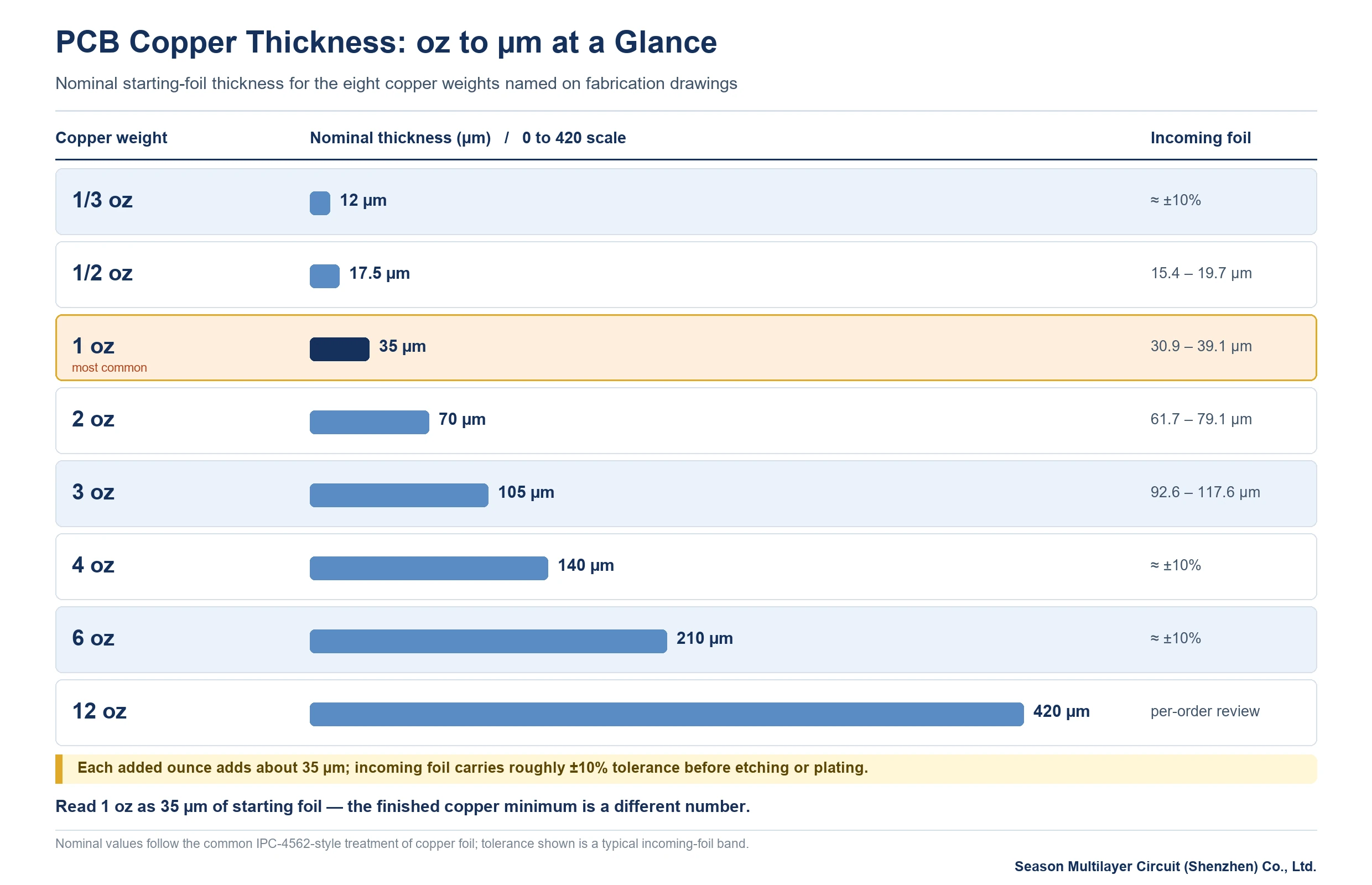
The 1 oz copper in µm conversion is linear: each additional ounce adds about 35 µm of nominal thickness. The PCB copper thickness table below adds the incoming-foil tolerance band, because the foil you receive is never exactly nominal. Values follow the common IPC-4562-style treatment of copper foil, in which thin foils run a tolerance of roughly ±10% around nominal.
| Nominal copper weight | Nominal thickness | Typical incoming foil range |
|---|---|---|
| 1/3 oz | ≈ 12 µm | ≈ ±10% |
| 1/2 oz (0.5 oz) | 17.5 µm | ≈ 15.4 – 19.7 µm |
| 1 oz | 35 µm | ≈ 30.9 – 39.1 µm |
| 2 oz | 70 µm | ≈ 61.7 – 79.1 µm |
| 3 oz | 105 µm | ≈ 92.6 – 117.6 µm |
| 4 oz | 140 µm | ≈ ±10% |
| 6 oz | 210 µm | ≈ ±10% |
| 12 oz | 420 µm | per-order review |
Two readings of this PCB copper thickness table matter for design. First, 1 oz foil can legitimately arrive at 30.9 µm and still be conforming incoming material — so a current-capacity calculation based on a full 35 µm has already consumed part of its margin before the first process step. Second, the tolerance applies to the starting foil only; plating and etching change the number again in opposite directions depending on the layer, which is the subject of the next section.
Base Copper vs Finished Copper: Which Number Is on Your Drawing
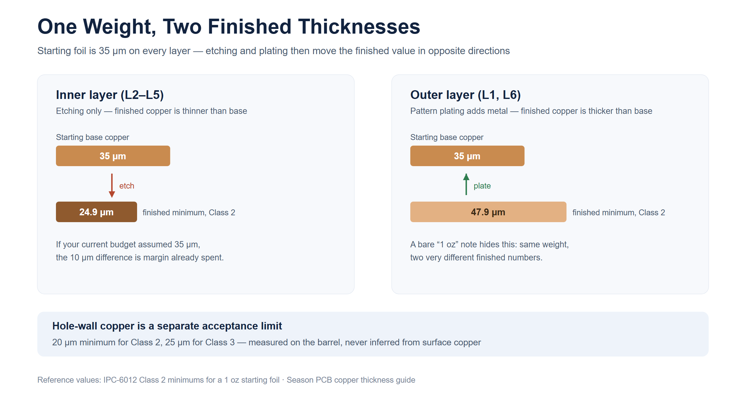
Base copper is the foil thickness bonded to the laminate as supplied by the laminate maker. Finished copper is the metal actually present on the completed board after electroless deposition, electroplating and etching are done. Every fabrication drawing should resolve base copper vs finished copper, because the finished value moves in opposite directions on different layers.
Inner layers only experience etching, so they only lose metal: a 1 oz inner layer finishes below 35 µm, typically around 30 µm or less once the etch undercut and half-etch of the conductor edges are accounted for. Outer layers receive pattern plating on top of the foil, so they gain metal: a 1 oz outer layer finishes well above 35 µm after plating brings the conductor up to its final height. Reading a single “1 oz” note as one number for all layers is the single most common PCB copper thickness misunderstanding in quotation reviews.
This is also why a supplier cannot simply “add copper” to fix a thin cross-section result on an inner layer. The starting foil defines the ceiling for inner-layer finished thickness, so the callout in the next table is written as a minimum finished value tied to a starting foil, not as a free-floating number.
IPC-6012 Copper Thickness Minimums by Class
IPC-6012 copper thickness minimums are defined by class of equipment. The values below are the widely referenced minimum-acceptance figures for Class 2 (dedicated service electronics) and Class 3 (high-reliability electronics); rounding varies slightly between revisions, so confirm against the current issue of the standard before writing an acceptance criterion.
| Starting base copper | Inner-layer minimum (Class 2) | Outer-layer minimum (Class 2) | Outer-layer minimum (Class 3) |
|---|---|---|---|
| 1/2 oz (17.5 µm) | ≈ 11.4 µm | ≈ 33.4 µm | ≈ 38.4 µm |
| 1 oz (35 µm) | ≈ 24.9 µm | ≈ 47.9 µm | ≈ 52.9 µm |
| 2 oz (70 µm) | ≈ 55.7 µm | ≈ 78.7 µm | ≈ 83.7 µm |
Read the IPC-6012 copper thickness minimums as floors, not design targets. A 1 oz inner layer measuring 30 µm on a microsection is compliant for Class 2, but if the power budget assumed 35 µm the margin is already spent. Thermal and current calculations should therefore use the minimum, not the nominal. Class 3 also tightens other conductor rules, including a lower allowable thickness reduction and a higher fill requirement where holes are filled; the class system itself is summarized in our IPC Class 2 vs Class 3 guide, and the full standards landscape is indexed by the Global Electronics Association standards library.
Hole-Wall Copper Is a Separate Acceptance Limit
Plated through-hole barrels are judged independently of surface PCB copper thickness conductors. IPC-6012 sets the hole-wall plating minimum at 20 µm for Class 2 and 25 µm for Class 3, and because the barrel carries current between layers and survives thermal cycling, it is frequently the first feature to fail when plating is marginal. For back-drilled holes the remaining barrel wall still needs to meet its stated minimum after the drill removes the upper portion.
Our internal control holds hole-wall copper at no less than 25 µm, with back-drilled holes at no less than 20 µm, verified by cross-section analysis and recorded with electrical test data on a per-lot basis. Specify the hole-wall limit as its own line rather than folding it into a general copper note. A surface-copper measurement cannot substitute for a barrel measurement, and that distinction causes most first-article disputes.
When you review a supplier’s microsection report, check that the barrel measurement was taken at the mid-span of the hole wall, not at the knee where the barrel meets the land, where plating is naturally heavier and can mask a thin mid-span reading.
Choosing Copper Weight: Current Capacity and Trace Width
PCB copper thickness selection balances three variables: the current a trace must carry within its temperature-rise budget, how fine the geometry can be etched at that thickness, and the cost tier the weight falls into. The estimates below use a 10 mm wide trace as the reference geometry — a width typical of power buses rather than signal routing — and follow common industry estimating practice; for release-level calculations, run the trace through the IPC-2152 methodology, and confirm your laminate system’s recognition data on the UL Solutions site.
| Copper weight | Approx. current on a 10 mm trace | Typical use | Cost vs 1 oz |
|---|---|---|---|
| 1 oz (35 µm) | ≈ 4 – 5 A | Signal layers and general power planes | Baseline |
| 2 oz (70 µm) | ≈ 8 – 10 A | Power distribution, industrial and energy-storage rails | Typically +20 – 40% |
| 3 oz (105 µm) | ≈ 12 – 15 A | Power buses, motor-drive boards | Quoted per engineering review |
| 4 oz (140 µm) | ≈ 16 – 20 A | High-current modules, onboard power stages | Quoted per engineering review |
| 6 oz (210 µm) | ≈ 24 – 30 A | High-power boards with integrated thermal structures | Quoted per engineering review |
| 12 oz (420 µm) | ≈ 45 A and above | Special ultra-high-current structures | Sample and small-batch, per review |
At the fine end, 1/3 oz and 1/2 oz foils exist for thin inner-layer geometry, not for current: at those weights a 10 mm trace is irrelevant, and the constraint becomes how fine the etch can hold lines — our process holds 2/2 mil line and space in production (1.8/1.8 mil on prototypes). Heavier copper narrows the achievable geometry at the same time as it widens the current budget, so the two requirements must be balanced inside one stackup. Layer-order implications are covered in our PCB stackup design guide.
Heavy Copper: What 3 oz and Above Require From the Fabricator
From roughly 3 oz upward, PCB copper thickness moves from a selection column to a process capability discussion. Heavier foils need wider etch allowances, steeper sidewall management to control undercut, and press cycles verified for the thicker metal; the stackup must stay balanced so the added copper does not warp the panel. This is why heavy-copper quotations are issued after an engineering review of the actual layer pairings rather than from a rate card.
Our production window covers 1/3 oz through 6 oz as a routine mass-production range, and we support heavy copper up to 12 oz (420 µm) for sample and small-batch builds with a per-order engineering review covering stackup symmetry, etch compensation and lamination feasibility. Design context for these builds — when heavy copper earns its cost and how it interacts with plane spacing — is laid out in our heavy copper PCB design rules, and the laminate-side considerations sit in our PCB materials and laminates pillar guide.
If your design needs 12 oz-class current but not 12 oz geometry, an alternative worth pricing is a copper pour combined with solder-coated conductors or busbar structures, which the same review can evaluate against a straight heavy-copper build.
How to Write PCB Copper Thickness on a Fabrication Drawing
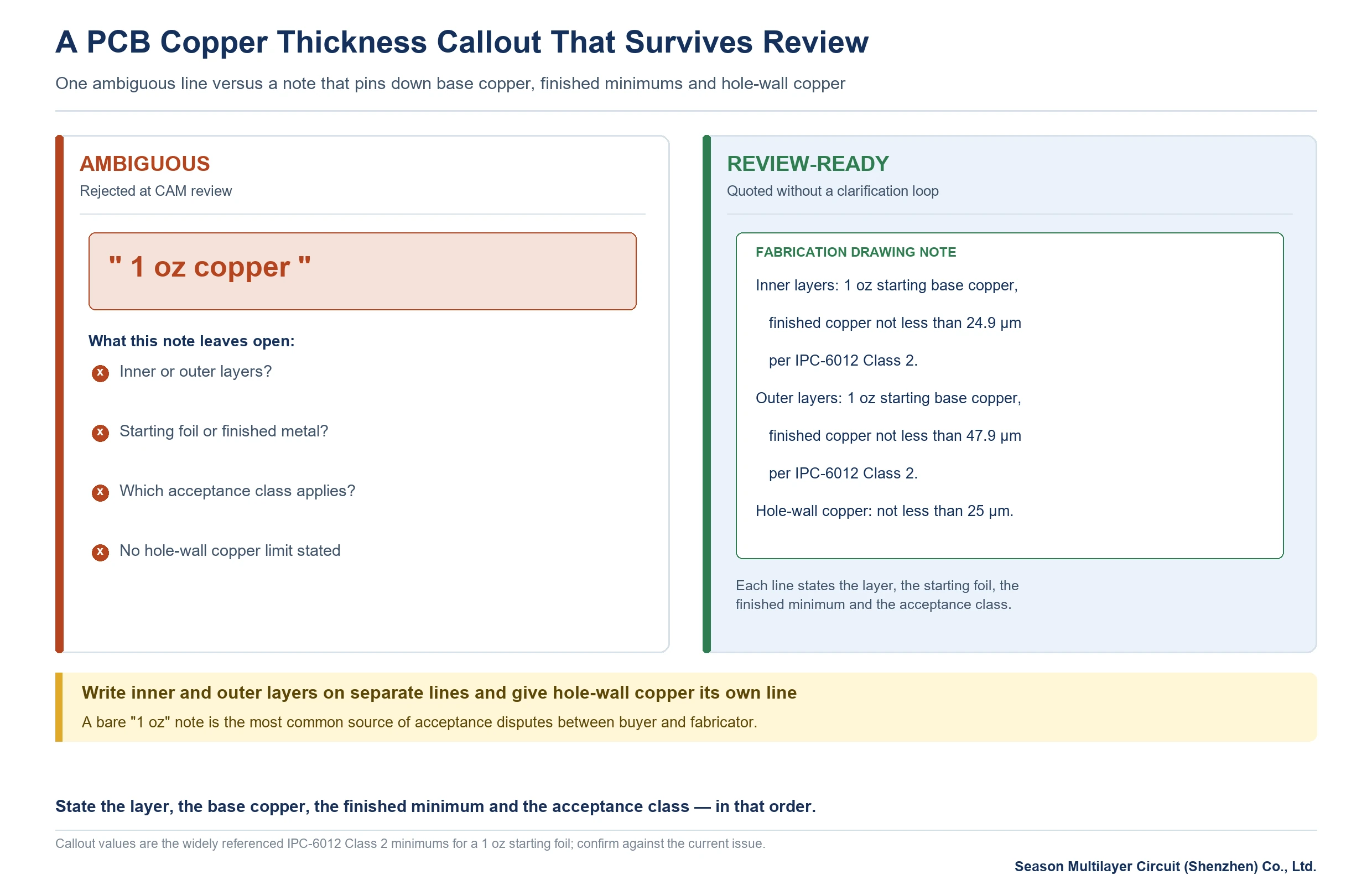
Ambiguous PCB copper thickness notes are the leading cause of rework loops between buyer and fabricator. Three failure patterns cover almost every dispute: a bare “1 oz” that never distinguishes inner from outer layers; a “heavy copper” note without a numeric weight, which leaves 2 oz and 3 oz priced differently by different suppliers; and a finished-value note with no starting foil, which plating cannot reverse-engineer.
- State whether each layer is specified as starting base copper or finished copper.
- Give the specific weight (oz) or the µm value — never just the word “heavy”.
- Attach the acceptance class (for example, IPC-6012 Class 2) so the minimum is unambiguous.
- Write inner and outer layers as separate lines, since their finished values differ.
- List hole-wall copper as its own line item with its own minimum.
A callout you can adapt directly: “Inner layers: 1 oz starting base copper, finished copper not less than 24.9 µm per IPC-6012 Class 2. Outer layers: 1 oz starting base copper, finished copper not less than 47.9 µm per IPC-6012 Class 2. Hole-wall copper: not less than 25 µm.” This wording survives quotation, cross-section inspection and first-article sign-off without translation between parties.
PCB Copper Thickness Acceptance Testing and Records
PCB copper thickness acceptance rests on two evidence streams. Cross-section analysis measures finished conductor and hole-wall thickness against the IPC-6012 copper thickness minimums and is the deciding record when a dispute arises. Incoming foil certificates tie the starting base copper to the supplier’s measurement, closing the loop between what was ordered and what entered the process. Boards with current-carrying requirements should additionally have their power paths covered by the electrical test plan, and high-reliability builds benefit from the qualification tests described in our PCB reliability testing guide.
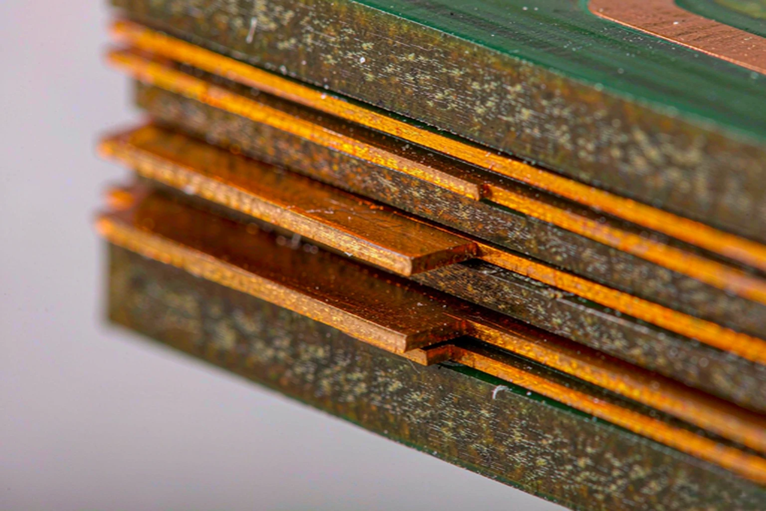
The layered-stack cross-section at the top of this article is what a healthy record looks like: alternating copper and dielectric layers with clean interfaces, plated barrels meeting their minimum, and measurement locations documented. When these records ship with the lot — as they do on builds run through our quality inspection and reporting process — acceptance stops being an argument about whose meter is right and becomes a comparison against stated limits.
Frequently Asked Questions
How thick is 1 oz copper in µm?
One ounce of copper over one square foot is approximately 35 µm thick. The scale is linear: 2 oz is about 70 µm, 3 oz about 105 µm, and half an ounce about 17.5 µm. Incoming foil carries a tolerance, so 1 oz foil can arrive between roughly 30.9 and 39.1 µm and still be conforming material.
What is the difference between base copper and finished copper?
Base copper is the foil thickness bonded to the laminate as it arrives from the laminate supplier. Finished copper is the metal left on the completed board after plating and etching. Inner layers only lose metal through etching, so finished is below base; outer layers gain metal through pattern plating, so finished is above base.
What is the minimum finished copper thickness for IPC-6012 Class 2?
For a 1 oz starting foil, the commonly referenced Class 2 minimums are about 24.9 µm on inner layers and about 47.9 µm on outer layers. Values shift slightly between revisions of the standard, so confirm against the current issue before writing an acceptance criterion into a drawing.
Is 30 µm acceptable on a 1 oz inner layer?
Yes for IPC-6012 Class 2, whose inner-layer minimum for 1 oz starting foil is about 24.9 µm. The caveat is design margin: if current capacity and thermal calculations assumed a full 35 µm, a 30 µm result means part of that margin was consumed by etching. Revisit the calculation against the measured value.
What hole-wall copper thickness does IPC-6012 require?
IPC-6012 sets the hole-wall plating minimum at 20 µm for Class 2 and 25 µm for Class 3. Our internal control holds hole-wall copper at no less than 25 µm, with back-drilled holes at no less than 20 µm, verified by cross-section and recorded per lot with electrical test data.
How much more does 2 oz copper cost than 1 oz?
As a relative figure, 2 oz typically adds roughly 20–40% over 1 oz, influenced by layer count, quantity and surface finish. Three ounces and above fall into the heavy-copper tier, where cost is established through an engineering review of the specific stackup rather than a fixed increment.
How heavy can copper go on a production board?
Our routine mass-production range runs from 1/3 oz through 6 oz. Heavy copper up to 12 oz (about 420 µm) is supported for sample and small-batch builds with a per-order engineering review covering stackup symmetry, etch compensation and lamination feasibility.
How should I write copper thickness on a fabrication drawing?
State whether each layer is starting base copper or finished copper, give the specific oz or µm value, and attach the acceptance class. Write inner and outer layers on separate lines and give hole-wall copper its own line item — a bare “1 oz” note is the most common source of acceptance disputes.
Get Your Copper Callouts Reviewed Before the Build
Send your Gerber package and stackup with the copper weight, acceptance class and hole-wall minimum you intend to specify — start from our PCB manufacturing services page. Our engineering team will confirm the finished-thickness values are achievable in your layer configuration before quotation, including heavy copper above 6 oz. Production runs from 2 to 30 layers (up to 64 layers for prototypes, subject to per-order review), and process feedback typically comes back the same day. You can also request an instant PCB quote with the copper callout attached.
Season PCB direct: Tel (+86) 18681528532 | WhatsApp +86 18681528532
E-mail: roc@season-pcb.com