Book Appointment Now

8-layer 2-stage (2+4+2) HDI SSD PCB on low-loss FR-4 for NVMe and SATA storage: 0.10 mm POFV blind vias, 3/3 mil lines, ±5 mil length matching, ENIG with hard gold fingers.
8-Layer 2-Stage High-Speed SSD PCB Manufacturer for NVMe and SATA Storage
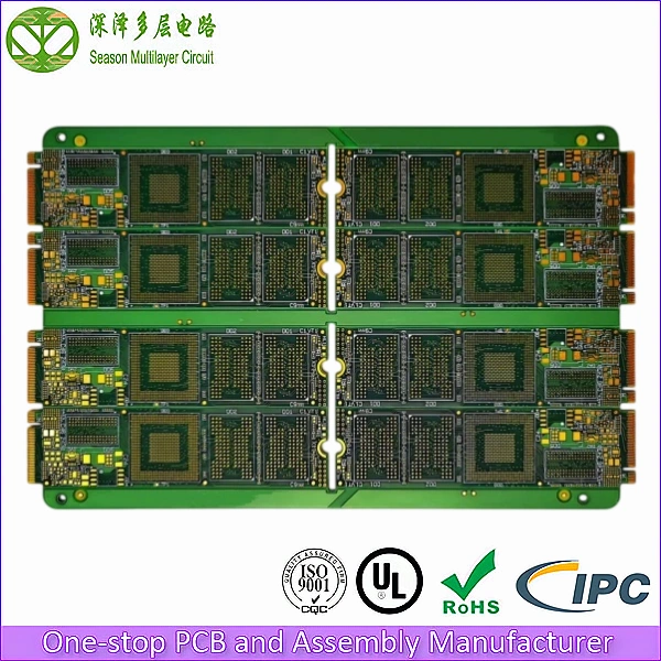
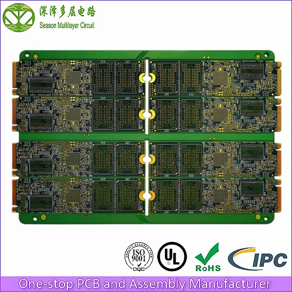
This high-speed SSD PCB is custom-built from your Gerber data on an 8-layer 2-stage (2+4+2) low-loss construction: two laser microvia build-up layers on each face of a four-layer core, 0.10 mm blind vias processed POFV under the controller and NAND ball-outs, 3/3 mil geometry on length-matched differential pairs, and ENIG with hard gold fingers at the slot edge. This page covers the reference high-speed SSD PCB build quoted for 6 to 16 Gbps NVMe and SATA storage channels; the full line is listed in our PCB products catalog.
Every board from this high-speed SSD PCB line is laminated in two sequential cycles with X-ray registration and coupon checks between them, so process drift is caught at the layer level. Stackup design, impedance control, POFV processing and the ENIG-plus-gold-finger finish are archived at order entry: the board you qualified as a prototype is the board you receive in volume — same recipe, same controls, same records.
Send Gerber RS-274X or ODB++ data with your stackup for a free DFM review with current-carrying and impedance calculations, and a formal quotation typically within 24 hours of a complete package. If your program also needs a rigid 2-stage platform beyond storage, the 12-layer 2-stage HDI core board covers that process.
2+4+2
Build-Up Stackup
0.10 mm
Min Laser Blind Via
3/3 mil
Line / Space
0.8 mm
Thin Board Thickness
ENIG 2µ”
Surface Finish
ISO9001-2004
ISO14001
UL (E305905)
IPC-Class 2/Class 3
IATF 16949
RoHS
What an 8-Layer 2-Stage HDI SSD PCB Is
An HDI SSD PCB is the carrier that keeps a storage controller and its NAND flash talking at full speed. This build is custom-fabricated from your Gerber on an 8-layer 2-stage HDI construction (2+4+2): two laser microvia build-up layers on each face of a four-layer core, in a 0.8 mm thin-board format selected for the 6 to 16 Gbps differential channels that NVMe and SATA interfaces demand.
The 2-stage HDI designation, also written as second-order or 2+N-2 HDI, means two sequential laser microvia build-up cycles on each outer side of the core. Signal layers connect through stacked microvias across multiple dielectric layers; the via mechanics behind this build are explained step by step in our HDI PCB technology guide.
In the standard build, the 2+4+2 stackup places two HDI build-up layers on each side of the four-layer core. Laser-drilled 0.10 mm blind vias reach L1–L3 and L6–L8 as two stacked stages (stage-1 vias L2→L3 and L6→L7, stage-2 vias L1→L2 and L7→L8) and are processed POFV where the controller and NAND ball-outs land on via-in-pad sites; mechanically drilled 0.15 mm through-vias stitch all eight layers. Low-loss TU-872SLK laminate holds insertion loss in check across SATA 6Gbps and PCIe Gen3/Gen4 storage lanes, and the symmetric construction keeps the thin board flat through reflow.
The lighter builds in the same storage family are the 4-layer SATA SSD PCB and the 10-layer M.2 SSD PCB; this page focuses on the 8-layer 2-stage HDI platform where via-in-pad and length matching are the qualification gates. For the full HDI capability from 1-stage to any-layer, see the Any-Layer HDI PCB page.
High-Speed SSD PCB vs Standard Storage Board: What the Extra Engineering Buys
A storage board fails in the field in predictable ways: an eye diagram that closes at temperature, a voltage droop during simultaneous NAND programming, or a module that stops seating after a few dozen insert cycles. The comparison below is what the 8-layer 2-stage high-speed SSD PCB construction buys against a conventional storage board — and that is exactly what the 1.3–1.6× cost factor purchases in field margin.
| Factor | 8-Layer 2-Stage HDI SSD PCB | Standard Storage Board |
|---|---|---|
| Signal rate | 6–16 Gbps differential (NVMe / PCIe Gen3–Gen4) | 480 Mbps – 5 Gbps |
| Length matching | ±5 mil intra-pair | ±10 mil typical |
| Material grade | Low-loss FR-4 (TU-872SLK class) | Standard FR-4 |
| Via technology | 0.10 mm laser blind vias, 2× POFV via-in-pad | Mechanical through vias only |
| Gold finger process | Hard gold with bevel and hardness control | Basic plating |
| Cost factor | ≈1.3 – 1.6× | 1.0 |
If your product sits below PCIe Gen3 speeds and does not need via-in-pad, a standard construction may serve you at lower cost — our engineers will say so at DFM review rather than upsell the second stage.
2-Stage vs 1-Stage HDI: When the Second Stage Pays Off on a Storage Board
Not every high-speed SSD PCB needs two lamination cycles. The honest answer we give storage teams: 1-stage is the right tool below a certain density threshold, and paying for the second stage below it is waste. The table below frames the decision.
| Attribute | 1-Stage HDI (1+N-1) | 2-Stage HDI (2+N-2) |
|---|---|---|
| Microvia reach | L1 to L2 only | L1 to L3 stacked (or staggered) |
| BGA breakout | Comfortable at 0.5 mm pitch and above | Routable at 0.25–0.4 mm pitch |
| Routing density | Standard HDI density | Substantially higher escape density |
| Lamination cycles | One | Two, with via fill + planarization between |
| Typical use | SATA 6Gbps drives, eMMC modules, mid-density boards | NVMe Gen3/Gen4 drives, via-in-pad controller layouts |
| Relative cost | Base | Premium justified by density or via-in-pad |
On this 8-layer platform the second stage is usually worth it: the controller and NAND ball-outs sit on 0.25 mm pitch sites that need via-in-pad, and the two POFV cycles keep those pads flat for mounting. If your drive is a SATA 6Gbps design without via-in-pad, a lighter build holds the same channel margin at lower cost — the 4-layer SATA SSD PCB page covers that path.
Technical Specifications of the 8-Layer 2-Stage HDI SSD PCB
The table below is the as-built specification for this high-speed SSD PCB reference construction. Your design is quoted against it and confirmed at engineering review.
| Parameter | Specification | Notes |
|---|---|---|
| Layer count | 8 layers, 2-stage HDI (2+4+2) | Two laser stages per side, mirrored |
| Base material | FR-4 TU-872SLK (low-loss grade) | Selected for 6–16 Gbps signal margins |
| Board thickness | 0.8 mm | Symmetric stack for warp control on thin boards |
| Panel format | 162 × 105 mm working panel, 4-up | Edge rails with tooling holes and fiducials |
| Outer copper | 1 oz (35 µm) | Foil plus plating |
| Inner copper | 1 oz (35 µm) | Power/ground and signal layers |
| Min through via | 0.15 mm | Through L1–L8 |
| Buried via | Mechanical | L3–L6 in the four-layer core |
| Min blind via | 0.10 mm | Laser-drilled, L1-L3 / L6-L8, two stages, POFV processed |
| Line / space | 3 / 3 mil | High-speed differential pairs length-matched ±5 mil |
| Min BGA pitch | 0.25 mm | Via-in-pad with POFV |
| Special process | 2× POFV (plated over filled via) | Via-in-pad for controller and NAND ball-out |
| Surface finish | ENIG 2 µ” Au + hard gold fingers | Beveled fingers, slot-tolerance controlled |
| Signal speed | 6 – 16 Gbps differential channels | NVMe / SATA 6Gbps and PCIe Gen3/Gen4 storage lanes |
| Quality standard | IPC-A-600 Class 2/3 per drawing | Test report and records ship with every batch |
| Quality system | ISO 9001:2015 · IATF 16949 | UL recognized laminate systems, RoHS & REACH |
Final high-speed SSD PCB parameters are confirmed per drawing during DFM review. Impedance targets, length-match windows and gold-finger geometry are agreed before tooling is cut.
The 2+4+2 Stackup of This HDI SSD PCB
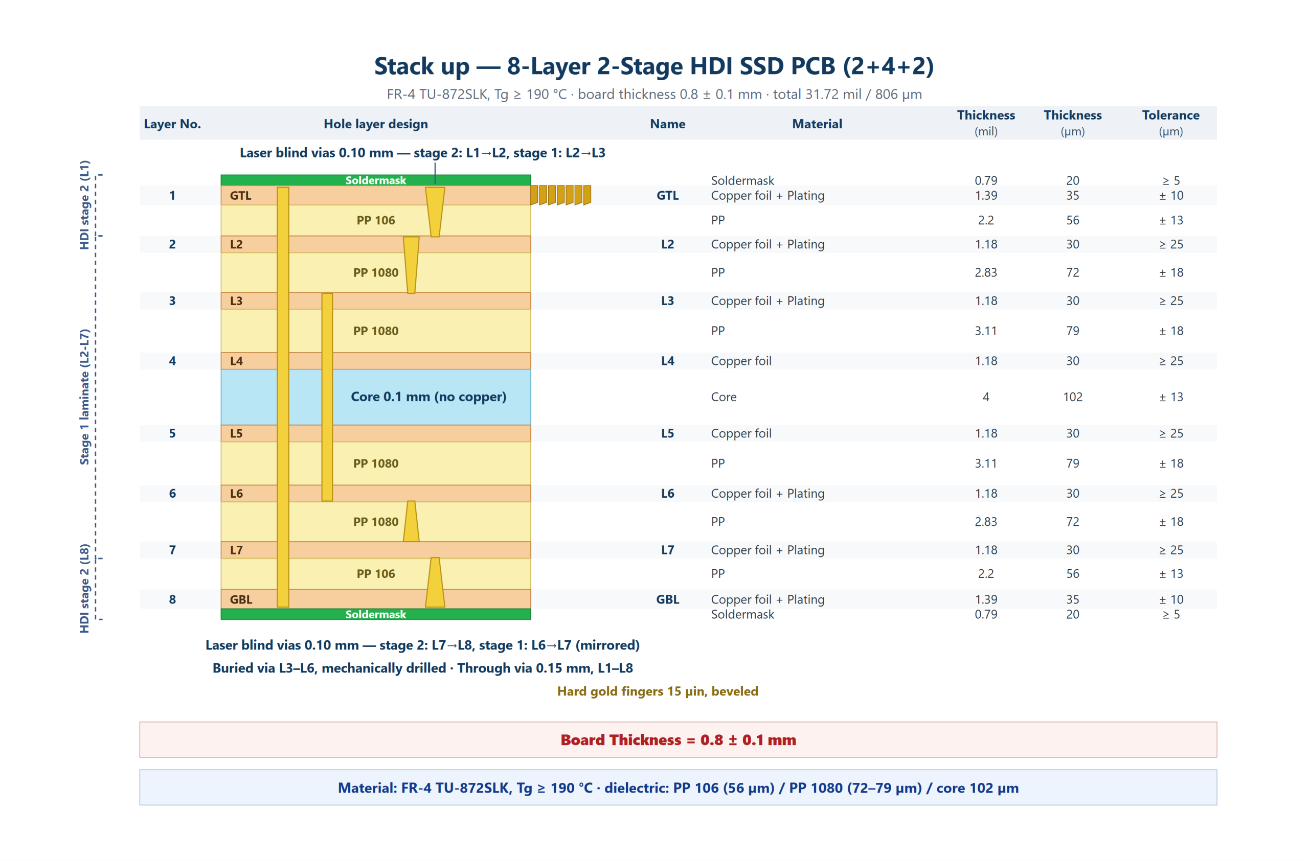
Two laser build-up layers sandwich the four-layer core on each side. Blind 0.10 mm microvias interconnect L1→L3 and L6→L8 through stacked stage-1 and stage-2 vias; controller and NAND ball-outs land on via-in-pad sites processed with two POFV cycles; and the hard gold fingers that terminate the L1/L2 fan-out at the slot edge are beveled for smooth insertion into the M.2 or SATA connector.
Exact dielectric thicknesses, copper weights and via structures are defined per high-speed SSD PCB design in the engineering build-up file issued for approval before tooling.
- L1 / L8 outer build-up — second HDI stage: laser-drilled 0.10 mm microvias, copper filled and planarized before outer foil lamination.
- L2 / L7 build-up stage 1 — first laser cycle over the core, giving L2→L3 and L6→L7 blind interconnects; stage 2 then stacks L1→L2 and L7→L8 vias over them, both cycles POFV-processed at pad sites.
- L3–L6 four-layer core — low-loss TU-872SLK FR-4 carrying the power/ground pairs and the length-matched differential signal layers, drilled with L3–L6 buried vias before lamination.
- Through-hole stitching — mechanically drilled 0.15 mm through-vias connect all eight layers for control and test nets.
- Via-in-pad with POFV — controller and NAND ball-out pads sit on filled, plated-over microvias for flat, mountable sites.
- Hard gold fingers — beveled edge-connector pads plated hard gold over nickel, pitch controlled against standard M.2/SATA slot tolerances.
What Makes This 8-Layer 2-Stage HDI SSD PCB Exceptional
8 Layers, 2+4+2 Build-Up
Two laser stages per side over a four-layer core, mirrored around the centerline to keep the 0.8 mm board flat through reflow.
0.10 mm Laser Blind Vias
Stage-1 blind vias (L2→L3, L6→L7) and stage-2 blind vias (L1→L2, L7→L8), laser-drilled, copper-filled and planarized before the next stage runs, giving L1→L3 and L6→L8 reach.
POFV Via-in-Pad
Two plated-over filled via cycles give controller and NAND ball-out sites flat pads at 0.25 mm pitch.
3/3 mil Line and Space
Geometry that supports the length-matched differential pairs NVMe and SATA storage channels are quoted against.
±5 mil Length Matching
Intra-pair matching with an unbroken reference plane preserves eye-diagram margin to 16 Gbps.
TU-872SLK Low-Loss Laminate
Low-Dk, low-Df FR-4 class that holds insertion loss inside budget at Gen4 storage speeds.
0.8 mm Thin-Board Construction
Symmetric copper and dielectric distribution keeps the thin high-speed SSD PCB inside flatness limits per drawing.
Hard Gold Fingers, Beveled
Edge connectors plated hard gold over nickel with hardness control, so the module seats cleanly cycle after cycle.
Three Design Problems Every High-Speed SSD PCB Must Solve
A storage board fails in the field in predictable ways. Building the answers into your layout from the start keeps the DFM review short and the qualification plan predictable for the high-speed SSD PCB build.
Signal Integrity on 6–16 Gbps Channels
The NVMe/SATA differential pairs carry length matching within ±5 mil with an unbroken reference plane under every pair. The low-loss TU-872SLK laminate keeps insertion loss in check across the channel, preserving eye-diagram margin at both SATA 6Gbps and PCIe Gen3/Gen4 storage speeds. Blind via stubs are eliminated by the 2-stage construction — the laser vias stop exactly where they should, with the acceptance criteria of the IPC standards library as the shared reference.
Power Integrity Under Parallel NAND Programming
Storage controllers and NAND arrays draw large transient currents during parallel programming. The power distribution network uses low-impedance planes with decoupling placed against the measured transient profile — suppressing ripple and droop so read/write throughput stays stable under sustained load on this high-speed SSD PCB.
Thin-Board Warpage Control
At 0.8 mm, the board is thin enough to warp if the stackup is asymmetric. The symmetric 2+4+2 construction balances copper weights, dielectric thicknesses and coverage around the centerline, and the lamination profile is tuned for the thin high-speed SSD PCB construction — flatness holds through reflow per drawing.
Gold Finger Slot Compatibility
Gold-finger thickness and pitch are controlled against standard M.2 and SATA slot tolerances, with beveled finger edges so the module inserts cleanly, hundreds of cycles over, without scraping the connector. Finger geometry is confirmed at DFM against your host connector drawing.
Why TU-872SLK for a High-Speed SSD PCB
At 6 to 16 Gbps, insertion loss through the laminate becomes a first-order design constraint. Standard FR-4 dissipates enough signal energy at these speeds to eat eye margin; the TU-872SLK class of low-loss FR-4 lowers both Dk and Df so channels hold their margins through the full operating temperature range — at a cost point far below specialist RF materials.
| Zone / Role | Default Material | Why It Is Chosen |
|---|---|---|
| Base laminate | FR-4 TU-872SLK, low-loss grade | Low Dk and Df for 6–16 Gbps margins, mainstream manufacturing behavior |
| HDI build-up dielectric | Laser-drillable prepreg | Clean CO2 laser ablation for 0.10 mm blind vias |
| Surface finish | ENIG 2 µ” + hard gold fingers | Solderability on pads, durable beveled edge connectors |
| Solder mask | LPI solder mask | Customer-specified color per drawing |
| High-speed option | Isola, Rogers, or Shengyi low-loss systems | For faster channel plans or mandated laminate lists |
The material also machines and laminates like production-grade FR-4: it drills cleanly at 0.15 mm through vias and ablates predictably under the CO2 laser for the 0.10 mm blind vias. If your channel plan runs faster than PCIe Gen4, or your qualification plan specifies a particular laminate brand, we substitute at stackup review — Isola, Rogers and Shengyi low-loss grades are all in routine use on our lines.
High-Speed Laminate Options: M4 to M9 Grades
Laminate is chosen by insertion loss, not by brand. The table below lists the high-speed laminate grades we stock and qualify for high-speed SSD PCB builds, from M4-class FR-4 through M9-class hydrocarbon and quartz-cloth systems — the Tu-872SLK grade used in the standard build above sits in the M4 group. Every row is a material we can run on our own lamination lines, so the grade selected at quotation is the grade that ships.
| Material Grade | Supplier | Laminate Model | Resin System | Dk (1 GHz) | Df (1 GHz) | Tg (°C) | Td (°C) | Z-CTE (%) | T28 (min) | Water Absorption (%) |
|---|---|---|---|---|---|---|---|---|---|---|
| M4 | SY | S7439C | FR-4 | 3.85 | 0.0045 | 190 | 383 | 2.60 | >60 | 0.08 |
| SY | S7439G | FR-4 | 3.93 | 0.0045 | 181 | 405 | 2.50 | >60 | 0.09 | |
| ITEQ | IT-170GRA2 | FR-4 | 3.80 | 0.008 | 180 | 380 | 2.70 | 30 | 0.10 | |
| TUC | Tu-872SLK | FR-4 | 3.77 | 0.008 | 200 | 340 | 2.30 | 20 | 0.15 | |
| TUC | Tu-863+ | FR-4 | 3.68 | 0.009 | 200 | 370 | 2.80 | 30 | 0.06 | |
| EMC | EM-526 | FR-4 | 4.00 | 0.005 | 230 (TMA) | 430 | 1.30 | >60 | 0.10 | |
| NY | NY3170M2 | FR-4 | 3.84 | 0.0056 | 170 (TMA) | 385 | 2.30 | >60 | 0.10 | |
| M6 | Megtron | R5775 (G) | PPO | 3.71 | 0.002 | 185 | 410 | 2.60 | >120 | 0.14 |
| SY | Synamic 6 | PPE | 3.70 | 0.0021 | 185 | 402 | 2.00 | 120 | 0.09 | |
| SY | Synamic 6GX | PPE | 3.87 | 0.0023 | 172 | 405 | 2.20 | >60 | 0.08 | |
| ITEQ | IT-968G | Modified PPO | 3.76 | 0.0034 | 175 | 400 | 2.30 | >60 | 0.15 | |
| TUC | Tu-883 | PPO | 3.60 | 0.003 | 220 | 420 | 2.50 | >60 | 0.08 | |
| EMC | EM-528 | BMI-modified resin | 4.00 | 0.0047 | 250 | 420 | 1.40 | >60 | 0.11 | |
| NY | NY6300 | PPO | 3.74 | 0.0027 | 190 | 400 | 2.30 | >120 | 0.12 | |
| M7 | Megtron | R578Y (GT) | PPE | 3.63 | 0.002 | 200 | 400 | 2.30 | >120 | 0.06 |
| SY | Synamic 8G | PPE | 3.62 | 0.0015 | 200 | 430 | 2.20 | >120 | 0.10 | |
| SY | Synamic 8GN | PPE | 3.55 | 0.0008 | 205 | 430 | 1.80 | >120 | 0.10 | |
| ITEQ | IT-988GSE | Modified PPO | 3.24 | 0.0013 | 190 | 405 | 2.90 | >120 | 0.26 | |
| EMC | EM-890K | Hydrocarbon + PPE | 3.10 | 0.0019 | 205 | 430 | 2.20 | >60 | 0.07 | |
| M8 | Megtron | R579Y (A) | PPE | 3.08 | 0.0012 | 220 (DMA) | 370 | 0.19 | >120 | 0.06 |
| SY | Synamic 9GN | Hydrocarbon resin | 3.25 | 0.0005 | 210 | 400 | 1.50 | >60 | 0.08 | |
| EMC | EM-892K | Hydrocarbon resin | 3.11 | 0.0014 | 215 | 420 | 1.80 | >60 | 0.07 | |
| EMC | EM-892K2 | Hydrocarbon resin | 3.00 | 0.001 | 215 | 420 | 1.80 | >60 | 0.07 | |
| M9 | Megtron | R2M59HA | Hydrocarbon + quartz cloth | 3.10 | 0.001 | ≥200 | >420 | |||
| SY | Synamic 10GQ | Hydrocarbon resin | 3.15 | 0.0007 | ||||||
| EMC | EM-896K3 | Hydrocarbon + quartz cloth | 2.70 | 0.0007 | 205 (DMA) |
Where This High-Speed SSD PCB Is Deployed
The 8-layer 2-stage high-speed SSD PCB platform serves storage products where via-in-pad and length matching decide qualification — the point where consumer, enterprise and embedded designs converge on the same construction.
Consumer and Surveillance SSD
M.2 2280/2242 and 2.5-inch SATA controller boards, plus NVR/DVR high-capacity write boards tuned for sustained multi-stream recording — the volume backbone of the category, where cost per unit and yield discipline decide competitiveness.
Enterprise Storage
Data-center NVMe drive boards and server storage daughter cards, where sustained-write thermal behavior and signal margin at Gen4 speeds are the qualification gates the high-speed SSD PCB platform is built around.
Embedded and Industrial Storage
eMMC modules and industrial PC storage boards that carry storage silicon into harsh environments with the same SI discipline and the same archived build recipe as the volume consumer lines.
Our Quality Guarantee: Six Inspection Gates from Imaging to Packing
Gate 1: Automated Optical Inspection
After every imaging step, AOI verifies the 3/3 mil geometry on every high-speed SSD PCB layer before it moves on.
Gate 2: POFV Fill Verification
Via fill level and pad planarization are verified on both POFV cycles before the sites are released.
Gate 3: TDR Impedance Coupon
A coupon on every high-speed SSD PCB panel is measured against the impedance model before the build is released.
Gate 4: Flying Probe and E-Test
The full netlist is compared against the Gerber source, and every board passes 100% electrical test with no sampling.
Gate 5: Micro-Section Analysis
Verifies blind-via fill, barrel copper and plating bonds at the layer level, not at final inspection.
Gate 6: Packing Records
Impedance coupon data, E-test report, micro-section photographs and the certificate of conformance travel with every batch.
Every batch from our lines ships with its record package: impedance coupon data, E-test report, micro-section photographs and the certificate of conformance. The full flow, from file review to packing, is described on our PCB manufacturing services page, and the equipment behind these numbers is listed on the manufacturing capability page.
From Gerber Data to Shipped High-Speed SSD PCB
Both lamination cycles of the high-speed SSD PCB are verified by X-ray registration and coupon testing before the next stage proceeds, so process drift is caught at the layer level, not at final inspection.
- 1. DFM review — stackup, via-in-pad sites, length-match windows and gold finger geometry checked against your data package.
- 2. Core lamination — the four-layer low-loss core is pressed with the power/ground pairs registered.
- 3. HDI stage 1 — laser drill, copper fill, planarization and POFV of the first build-up.
- 4. HDI stage 2 — second build-up cycle, X-ray verified before outer foil lamination.
- 5. Finish and test — ENIG, hard gold fingers, TDR coupon measurement and 100% electrical test.
- 6. Final QC — micro-section, dimensional audit and the batch acceptance package.
Why Order Your High-Speed SSD PCB from Season PCB
- Free engineering review for your high-speed SSD PCB before you commit. DFM review with current-carrying and impedance calculations on every inquiry — process risk is cleared before material is cut, not after a respin.
- HDI is an in-house core process. 1-stage and 2-stage build-ups run on the same lines as standard multilayer work, so the 2+4+2 lamination profile never changes hands mid-build.
- Parameters archived, recipes repeated. Engineering parameters for your part number are stored at order entry — prototype and volume are the same build by design.
- Audited quality system. ISO 9001:2015 and IATF 16949 quality systems, UL recognized laminate systems, RoHS and REACH compliance.
- Turnkey option. Bare board, or board plus PCBA — see PCB manufacturing services for how the two are split.
Storage-Focused HDI Production
Season PCB has run HDI storage boards since 2006 across three plants, on lines qualified for both lamination cycles.
2-Stage HDI at Production Yield
Blind-via fill and planarization are controlled between the two cycles, so yield does not depend on heroics at final inspection.
Length Matching Verified per Panel
Differential pairs are modeled and verified with a TDR coupon against the ±5 mil windows on every panel.
Batch Records with Every Shipment
Impedance coupon data, E-test reports, micro-section photographs and a certificate of conformance ship with each lot.
Prototype and Volume on One Line
NPI builds and production volumes run on the same qualified high-speed SSD PCB process, so the design does not drift between prototype and ramp.
One-Stop PCB + PCBA
Component sourcing and SMT for the assembled drive run under the same quality system, described on our PCB manufacturing services page.
The group behind this high-speed SSD PCB platform — its plants, equipment and capability envelope — is profiled in our 998 PCB Group manufacturer overview.
What to Send for a Same-Week High-Speed SSD PCB Quote
A complete data package is the single biggest accelerant for a high-speed SSD PCB quotation. Here is the checklist our quoting engineers work from:
- 1. Circuit data — Gerber RS-274X or ODB++, with the stackup requirement noted.
- 2. Stackup or build-up requirement — your target stackup, or just the constraints (0.8 mm thickness, impedance targets, layer count) and we propose the 2+4+2 build-up.
- 3. Impedance and length-match targets — net classes, values and ±5 mil windows if controlled.
- 4. Via-in-pad map — which ball-out sites are POFV, so the fill-and-plate cycles are quoted correctly.
- 5. Gold finger drawing — finger pitch, bevel and hardness calls against the host slot.
- 6. Acceptance class and quantity — IPC-A-600 Class 2/3 as applicable, prototype quantity and expected annual volume.
Send the package to this high-speed SSD PCB manufacturer via the quote button above or email it directly — a complete package is quoted typically within 24 hours, and incomplete packages get specific questions back within the same window. A formal NDA can be signed before any data exchange for programs that require it.
Frequently Asked Questions
What are the special requirements for gold fingers on an SSD PCB?
SSD edge connectors use hard gold plating over nickel, typically in the 0.4–1.0 µm gold class over a 3–6 µm nickel layer, with beveled edges so the module seats smoothly into the M.2 or SATA slot. Gold thickness and the finger-to-finger pitch are controlled against standard slot tolerances so the high-speed SSD PCB inserts without scraping the connector.
How do you keep a thin 0.8 mm PCB from warping?
Warp control on thin boards comes from a symmetrical stackup: copper weights, dielectric thicknesses and copper coverage are balanced around the board centerline, and the lamination profile is tuned for the thin construction. On this 8-layer 2+4+2 HDI build, symmetry plus a 4-up panel format keeps flatness inside IPC-A-600 limits through reflow.
What files are needed to prototype an 8-layer 2-stage HDI SSD PCB?
Send Gerber RS-274X or ODB++ data with the stackup requirement, and note the impedance targets for the high-speed differential pairs if controlled. We return a free DFM review with current-carrying and impedance calculations, then a formal quotation — typically within 24 hours of receiving a complete package.
What determines the price of a high-speed SSD PCB?
The main cost drivers are layer count and HDI stage (the two lamination cycles), the low-loss laminate grade a high-speed SSD PCB channel demands, panel utilization on the 162 × 105 mm working panel, via process (POFV adds a fill-and-plate cycle), gold finger plating area, and testing scope. Volume quantities amortize the HDI setup cost, so unit price drops sharply from prototype to batch.
What are the lead times for prototypes and volume production?
8-layer 2-stage HDI SSD PCB prototypes ship in 5 to 7 working days and volume orders in 15 to 20 working days. Other layer counts and process combinations are confirmed at engineering review.
Is volume production quality the same as the prototype?
Yes. Engineering parameters for every build are archived and controlled, so the prototype recipe is the production recipe. AOI, 100% flying-probe or ICT testing, first-article cross-sections and SPC control on critical steps run identically on both, and test reports ship with every batch.
Are Gerber files and design data kept confidential?
Yes. Customer design data is used only for fabrication, stored under controlled access, and never shared with third parties. A formal NDA can be signed before any data exchange for programs that require it.
Ready to Start Your 8-Layer 2-Stage HDI SSD PCB Project?
Send us your Gerber data and stackup requirements. The engineer who reviews your files returns a DFM review and a quotation from your high-speed SSD PCB manufacturer — typically within 24 hours.