Book Appointment Now

PCB DFM analysis screens your design against real fabrication limits before release. See the checks, a pre-send checklist and what the findings report looks like.
PCB DFM Analysis: What Gets Checked Before Your Gerbers Release
Most boards that fail in production do not fail because the fabricator made a mistake. They fail because a rule was stretched somewhere it could not hold. An annular ring broke out on one layer, an aspect ratio exceeded what the drill could plate, a copper pour ran closer to the panel edge than the process allows. A PCB DFM analysis exists to catch those decisions while they are still free to change, before tooling is ordered and before a date is committed.
This guide walks through what a manufacturability review actually screens, section by section, with the limits held in production here as the reference points. It ends with a checklist you can run on your own design before release, and a look at how the findings come back so they can be acted on quickly.
Table of Contents
- What PCB DFM Analysis Covers
- Why the Review Runs Before Release, Not After
- Trace, Space and Annular Ring Checks
- Via Rules: Drill Size, Aspect Ratio and Plating
- Stackup and Impedance Checks
- Panelization, Copper Balance and Edge Rules
- A Pre-Release Checklist Before You Send Gerbers
- What a PCB DFM Analysis Report Contains
- Why Early Findings Are Cheap and Late Ones Are Not
- How Deep Should the Review Go?
- FAQ
- Send the Design Data for a Manufacturability Review
What PCB DFM Analysis Covers
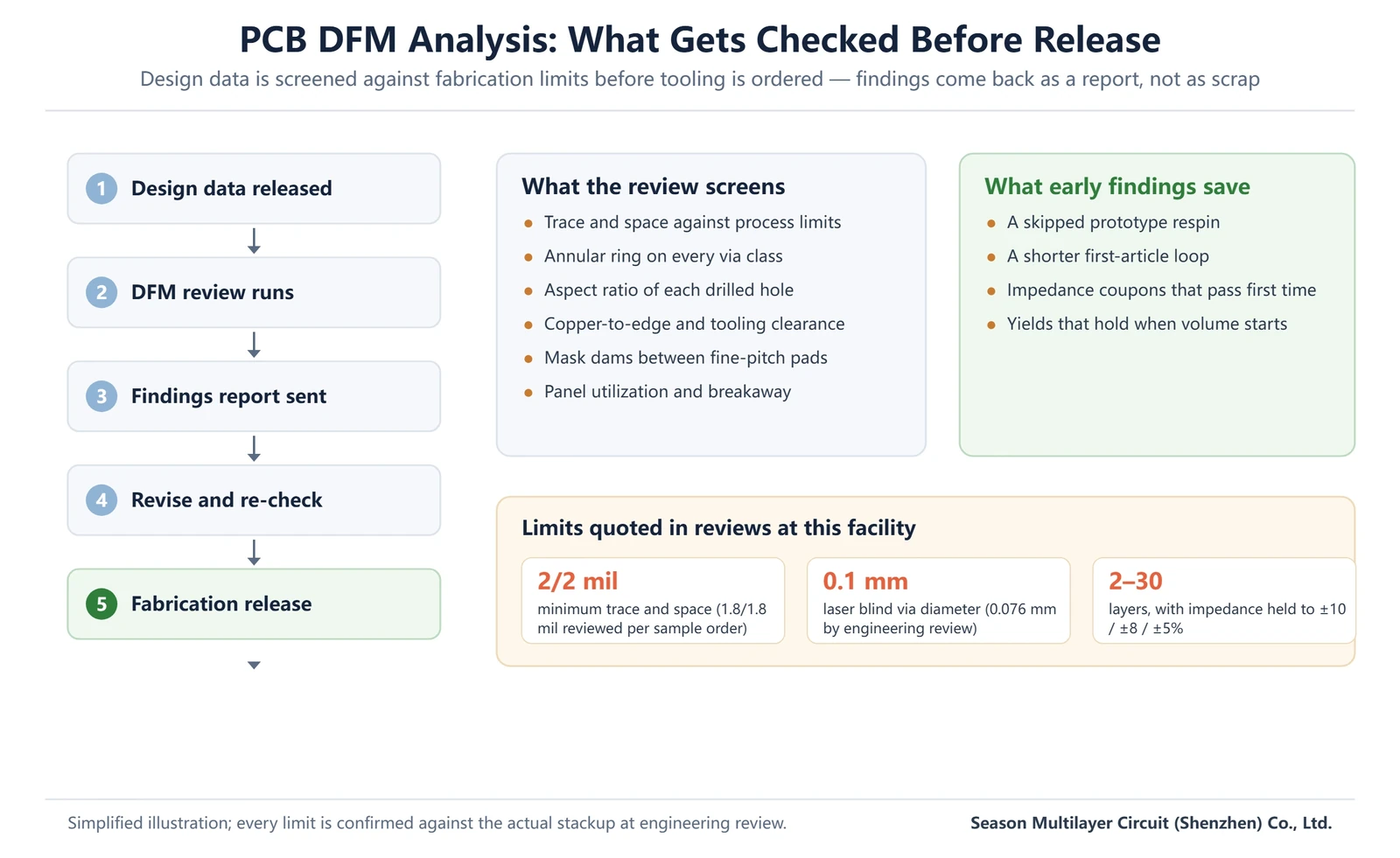
PCB DFM analysis is a structured screen of your design data against the process limits of the facility that will build the board. It is not a design review and not an electrical check. It asks one question repeatedly: can each feature on the board be fabricated at the stated layer count, material and finish, at yield? The screen runs on the same files the plant will tool from, so it sees the design exactly as production will.
A full review covers six families of checks. Trace and space against etch limits. Annular ring on every via class, on every layer. Drill size against aspect ratio and plating capability. Copper-to-edge and panel tooling clearances. Solder mask dams between fine-pitch features. And the economics of the panel itself: utilization, breakaway placement and scoring or routing strategy. Each family has a pass band, and anything outside it gets flagged with a severity and a suggested fix. Engineers sometimes describe this as a design for manufacturability PCB pass, and the two phrases name the same gate. A design for manufacturability PCB review reads the release set the way production will read it, so a PCB DFM analysis measures every feature against limits the facility holds in production rather than against drafting preferences. The output is a comparison, not an opinion. For buyers, the practical value is simple: a PCB DFM analysis answers the buildability question before money moves.
| Check family | What it screens | Typical finding |
|---|---|---|
| Trace and space | Etch capability against the thinnest features on every layer | 3/3 mil design quoted against a 2/2 mil process is safe; 1.5/1.5 mil needs review |
| Annular ring | Pad size versus finished hole on every layer of every via | Hole breaks out on an inner layer where registration drift stacks |
| Drill and aspect ratio | Hole diameter against board thickness and plating limits | 0.2 mm hole through a 2.4 mm board cannot plate reliably |
| Copper to edge | Clearance from pour and planes to board and panel edge | Plane at 0.2 mm from edge shaves during routing |
| Solder mask | Dam width between pads, mask alignment to features | No dam left between 0.4 mm pitch BGA pads |
| Panel economics | Utilization, breakaway, scoring versus routing | Odd board size forces a low-utilization panel and a cost step |
Why the Review Runs Before Release, Not After
The value of a manufacturability screen is entirely in its timing. Run after tooling, a finding becomes a change order; run after prototype, it becomes a respin with new tooling and a slipped schedule; run after production starts, it becomes scrapped panels and late orders. The same engineering observation costs almost nothing at release and a great deal later, which is why the review is positioned as a gate before quotation is confirmed rather than a service bolted onto it.
There is a second, quieter benefit. A review that runs on every release builds a shared vocabulary between the designer and the fabricator. After a few passes, the findings stop repeating: the design team internalizes where the process limits sit, and the data arrives clean. That is usually worth more than any single catch, because it removes the two-day question loop from every future build. It is also why a written DFM review checklist beats an unwritten habit: the checklist fixes the vocabulary, so a design for manufacturability PCB conversation starts from the same short list of questions on every project instead of being reinvented each time. For teams that send work out regularly, that shared PCB DFM analysis vocabulary is worth as much as any single catch. A PCB DFM analysis run before release keeps that vocabulary current.
This is also where fabricator selection quietly shows up. A supplier whose multilayer PCB manufacturing capability is published with explicit limits can answer manufacturability questions from a table. One that cannot will answer them from your first prototype, which is the expensive way to learn them.
Trace, Space and Annular Ring Checks
Etch limits are the most quoted process numbers and the most often misread. The figures that matter are held in production, not demonstrated once on a coupon: at this facility the production minimum is 2/2 mil trace and space, with 1.8/1.8 mil reviewed per sample order. A design drawn at exactly the minimum leaves no process margin. The review therefore asks a slightly different question than pass or fail: how much of the board sits at the limit, and on which layers.
Annular ring is where registration reality lives. Every drilled hole lands with some offset against the pad on each layer, and that offset grows with layer count and board thickness. The check sizes every pad against its finished hole per layer, and the inner layers are where designs typically fail. A pad that is comfortable on the outers can break out entirely on L3 of a thick stack. Where a ring cannot be widened, the fix is usually to relax the hole size or move to a via structure that tolerates the drift. Annular ring is the classic case where a PCB manufacturability check has to run per layer rather than once per design: the same via can sit comfortably on the outers and break out on L3, so the PCB DFM analysis reports the worst case instead of the average. That is also what separates a check from a DFM findings report: one records geometry, the other records severity and who has to act. Treat the PCB manufacturability check as a margin audit, not a pass/fail stamp.
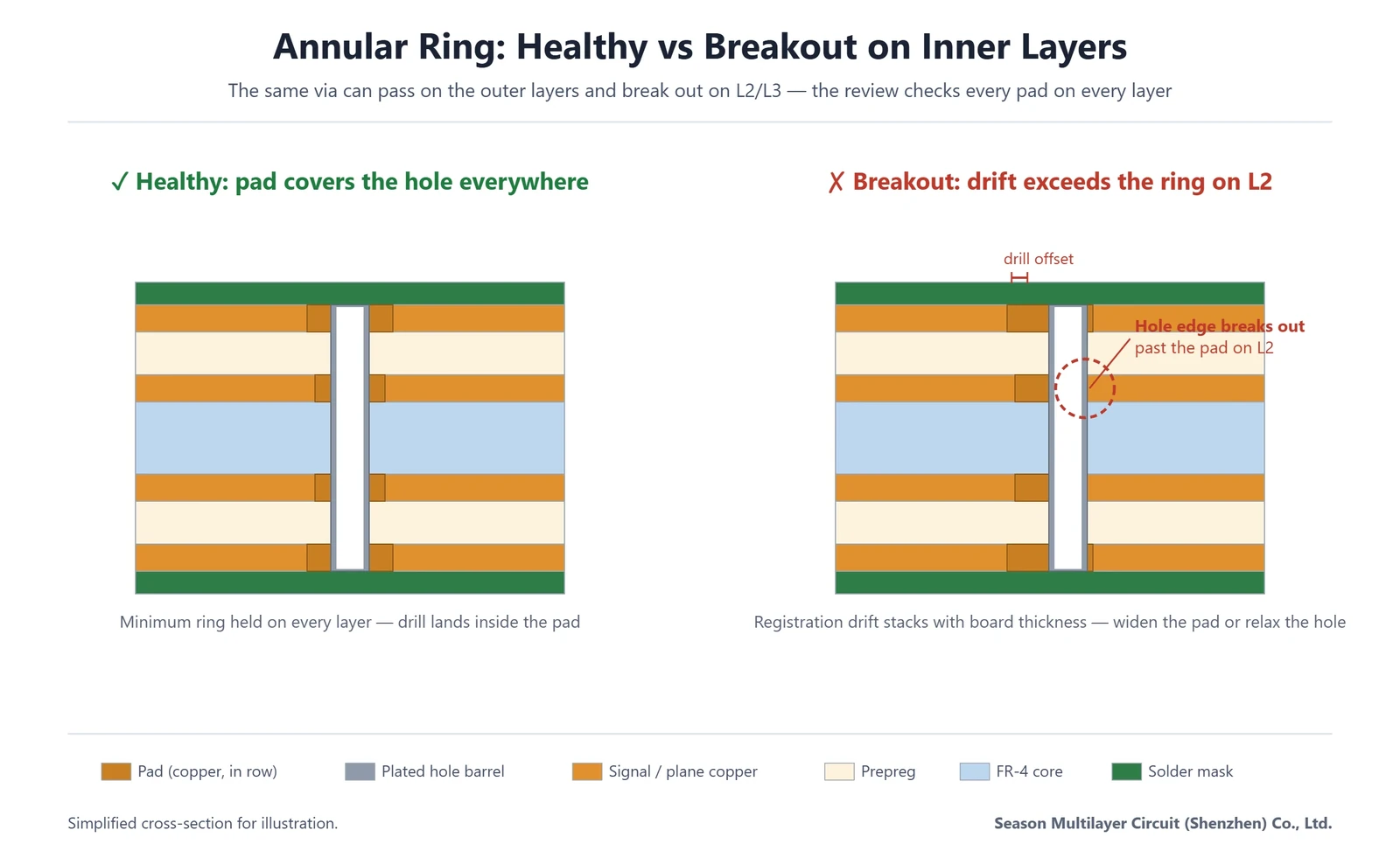
Both checks interact with impedance. A trace trimmed to survive etch at its minimum width shifts the impedance the stackup promised, so the review looks at the two together. If the impedance control plan depends on a trace sitting at the process minimum, that dependency is flagged before it reaches a TDR coupon measurement.
Via Rules: Drill Size, Aspect Ratio and Plating
Every drilled hole carries two numbers that must agree: the finished hole diameter and the board thickness it passes through. Their ratio, the aspect ratio, decides whether the hole can be plated uniformly from top to bottom. Push the ratio high and the plating thins in the middle of the barrel, which is a reliability defect that inspection cannot see after the fact. The check therefore pairs each hole class with the finished thickness of the stack it crosses, not with the nominal thickness on the drawing.
The review also separates hole classes that designs routinely blur. Through vias that carry no component are free to be larger and cheaper. Via-in-pad and filled structures carry plating and fill steps that add cycle time and cost, and they are only worth it where the layout genuinely demands them. Blind and buried vias add lamination cycles. Each class is checked against its own capability window, and mechanical versus laser drilling is assigned per class rather than assumed.
One output of this section is a via map: a short table of every hole class in the design with its diameter, pad, layer span and aspect ratio. It is the fastest way to spot the one oversized stack or the one undersized pad that would otherwise surface as a field failure. A via map also makes the design for manufacturability PCB conversation concrete. Instead of discussing holes in the abstract, you and the fabricator look at the same table and mark the classes a PCB manufacturability check would size first. The same page later attaches to the DFM findings report, so every severity in the PCB DFM analysis traces back to a row you have already read. In practice, the design for manufacturability PCB review and the via map settle most via questions in one pass.
Stackup and Impedance Checks
The stackup review reads the layer order, dielectric thicknesses and copper weights against three demands at once: the impedance plan, the symmetry of the press, and the current the planes have to carry. Asymmetric stacks warp in reflow; single-sided copper loading does the same. The fix is usually cheap at this stage, moving a plane or pairing a pour, and expensive at any later stage. That is why stackup findings carry high severity even when the board would technically build.
Impedance control is checked as a promise that can be held, not a number on a drawing. Each controlled pair or single-ended class is traced to the dielectric that sets it and to the tolerance the process can hold on that geometry. The standard band is ±10%, with ±8% and ±5% where the design justifies tighter control and the geometry supports it. The stackup design rules article covers the layer-planning side; the review checks that what was planned survives contact with the etch and press limits above. An impedance plan written into a DFM review checklist usually carries the class, the reference layer and the tolerance band together, and the review checks all three: a class promised at ±5% on a geometry the press cannot hold symmetrically is a finding even though every individual value on the drawing looks reasonable. A PCB manufacturability check on impedance is, in the end, a check on whether the promises the stackup makes can be held by the process that builds it, which is why the PCB DFM analysis treats the two documents as one. In short, the PCB DFM analysis asks whether the impedance promise survives the press.
Panelization, Copper Balance and Edge Rules
Every board is built on a panel, and the panel decision is made before your board is. Copper-to-edge clearance, tooling hole placement and the routing or scoring path all belong to the design data, so the review screens them rather than improvising around them. A plane that runs to the board edge risks exposure during routing; a pour that stops 0.5 mm short costs nothing and removes the risk entirely.
Utilization is the economic half of the same check. A board whose outline fits the standard production panel well builds at one cost step; a board slightly larger forces a bigger panel or a lower count. Panel economics is also where a DFM review checklist earns its keep on cost rather than on yield. Utilization, breakaway style and scoring versus routing set the price of every board in the job before the first etch tank is involved, so the PCB DFM analysis screens those decisions with the same seriousness as trace geometry, and the design for manufacturability PCB findings that come back usually pay for the review on the first order. A DFM findings report that names a better panel fit is worth more than a price negotiation. Because panel size and unit-set strategy are decided with the data, the review can often propose a breakaway or a small outline change that steps the cost back down before the quote is issued. At that point, the change costs the designer minutes instead of a revision.
A Pre-Release Checklist Before You Send Gerbers
Most findings repeat across designs, which makes them checklist material. Run the list below before releasing data; it takes minutes and clears the majority of routine review traffic. Items on a PCB manufacturability checklist are cheap to verify precisely because they are arithmetic: compare a number on the drawing with a published limit and record the margin. What the DFM review checklist cannot do is check interactions, which is why it complements rather than replaces the engineer-led pass that produces the DFM findings report. Between the arithmetic on the page and the PCB DFM analysis behind it, the two layers of screening cover what the file manager never will. A PCB manufacturability check scales its depth this way without changing its questions. The final item matters as much as the rest. Paste and fabrication layers copied from an older revision are a recurring source of first-article surprises, so verify the release set in the Gerber data itself rather than in the file manager.
- Confirm the thinnest trace and space on every layer against the stated process minimum, with margin, not at the limit.
- Check pad size per layer for every via class; look hardest at inner layers of thick stacks.
- Pair each hole diameter with the thickness of the stack it crosses and sanity-check the aspect ratio.
- Keep copper 0.5 mm or more from the board edge unless the outline is deliberately plated.
- Verify mask dams exist between fine-pitch pads at the finish you chose.
- State the controlled impedance classes and the tolerance band you expect on each.
- Balance copper top to bottom, and note any asymmetric region so the press can be planned for it.
- Confirm the release set: fab and assembly layers from the same revision, with the paste layer matching the stencil you intend to order.
The table version is worth keeping beside the release procedure, because each row names who can act fastest:
| Checklist item | Why it matters | Fastest fix |
|---|---|---|
| Trace and space margin | Etch at the limit shifts impedance and yield together | Widen the class or move it to a heavier-copper layer |
| Inner-layer annular ring | Registration drift stacks with thickness | Enlarge pad or relax hole; review via structure |
| Aspect ratio per stack | High ratios plate thin mid-barrel | Increase hole or reduce thickness; split the via |
| Copper-to-edge clearance | Routing shaves exposed plane edges | Pull pours back 0.5 mm |
| Mask dams | No dam means bridging at fine pitch | Open mask relief per pad instead of per window |
| Panel fit | Poor fit steps the cost and lead time | Adjust outline or accept a stated utilization |
What a PCB DFM Analysis Report Contains
A usable findings report is short and ranked. Each finding carries a location in the design, the rule it touches, the severity, and a suggested fix with its cost implication in relative terms. Severity is what makes the report actionable: without it, a designer facing twenty comments treats them all as equal and optimizes for closing the list rather than for the board.
| Severity | Meaning | Expected action |
|---|---|---|
| Blocking | The build as drawn cannot meet the stated spec or yield | Change before release; quote is held until resolved |
| High | Buildable but with a known yield or reliability risk | Change recommended; accepted risk must be stated in writing |
| Advisory | Cost or lead-time implication with no reliability risk | Designer’s call; noted on the quote |
The report also records the limits it screened against, so the findings are traceable to a published capability rather than to one engineer’s opinion. That matters when a finding is disputed: the conversation becomes about whether the rule applies to this build, not about what the rule is. Acceptance criteria on the finished board stay anchored to the IPC standards family, and the review’s job is to keep the design inside the band those criteria measure. A DFM findings report earns trust the same way: it names the limit it screened against, so a designer who disagrees can argue with a published number rather than with a person. Over a few builds, the DFM findings report stops being a gate you pass through and becomes a design tool you consult early, which is the quiet goal of every PCB DFM analysis. A design for manufacturability PCB review that ships with the quote is one you can actually plan around.
Why Early Findings Are Cheap and Late Ones Are Not
The economics of manufacturability findings follow a curve everyone in the industry recognizes and still underestimates. A rule violation caught in CAD costs a file edit. Caught at prototype, it costs a respin: new tooling, new boards, and a schedule slip measured in days. Caught in production, it costs scrap, re-ordered material and orders that ship late, and the reliability kind of finding may not surface until the field, where it costs the most of all.
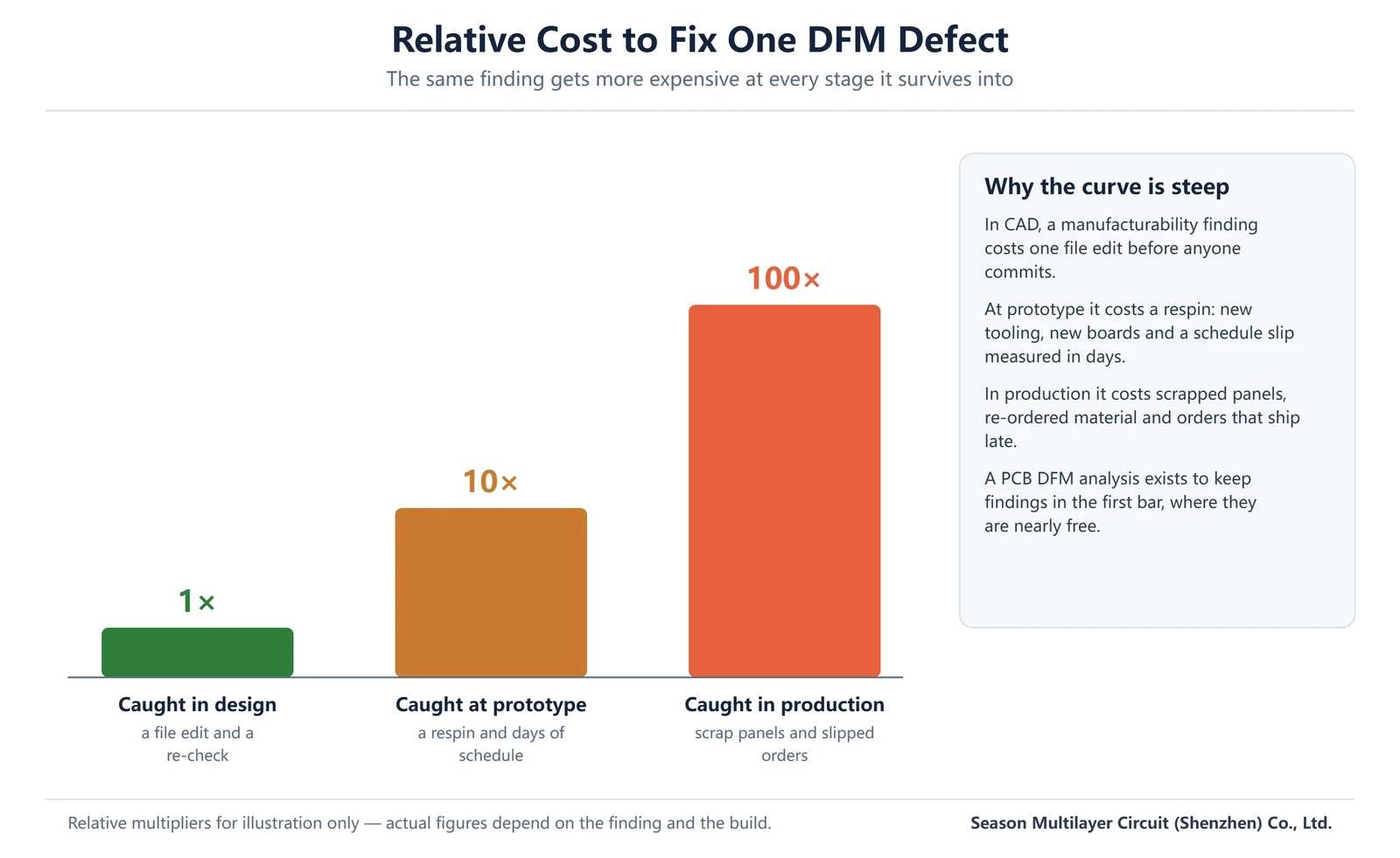
The multipliers in the chart are the usual rule-of-thumb ratios, not quotes, but the shape is what matters. It is also why the review is positioned before the quote rather than after the order. Findings returned with a quotation arrive while every option is still on the table. The designer can weigh a trace change against a stackup change against accepting the risk, with the full picture in front of them.
How Deep Should the Review Go?
Review depth should scale with how far the design sits from standard process territory. A four-layer FR-4 board with conventional geometry is fully screened by an automated pass plus a quote-level check; nothing more is needed, and padding the review wastes everyone’s time. Complexity moves the needle: high layer counts, tight impedance bands, filled or capped via structures, unusual materials and thick copper each add a manual pass by an engineer who has built that class before.
A practical rule: ask for the deep review when your design crosses more than one of the lines above, and ask for it at the same time as the quote, not after. One more distinction is worth keeping: the depth of a PCB DFM analysis scales with the build, but the design for manufacturability PCB intent behind it does not change. Every release deserves the same question (can this be built here, at yield, as drawn) asked before the files leave your desk, and any DFM review checklist you keep internally should end on exactly that line. That is the line every PCB DFM analysis in this series is written to. For an example of where this matters, the review that precedes a build like the 10-layer 2-stage HDI prototype covers sequential lamination, laser via capability and registration across the stack. Those decisions are effectively frozen once tooling starts.
Frequently Asked Questions
What is PCB DFM analysis?
It is a structured screen of your design data against the process limits of the facility that will build the board. The review checks trace and space, annular ring, drill aspect ratio, copper-to-edge clearance, solder mask dams and panel fit, then returns ranked findings with suggested fixes while the design is still free to change.
When should a DFM review run?
Before the design is released and the quote is confirmed. A finding returned at that point costs a file edit; the same finding after tooling costs a change order, and after prototype it costs a respin with a slipped schedule. Early is not a preference here, it is where all of the value sits.
Does PCB DFM analysis catch assembly problems too?
A fabrication review catches the bare-board issues; assembly adds its own layer, such as paste release on fine-pitch apertures, courtyard collisions and test-point access. Many fabricators run both screens when quoting turnkey work, and the bare-board review should at minimum flag the land patterns that will fight the assembly process later.
What files do I need to send for a manufacturability review?
The fabrication data you intend to build from: the Gerber or ODB++ set, the drill files, and the stackup or layer table with materials and thicknesses. Add the impedance classes and the tolerance band you expect, plus any special requirements. A review is only as good as the data behind it, so send the release set, not a working copy.
What is the difference between DFM and DRC?
Design rule checking in your CAD tool validates the design against the rules you loaded, which are usually generic or conservative. A PCB DFM analysis validates the same features against the specific limits of the facility that will build the board. It also catches interactions a rule file cannot see, such as whether a stack’s aspect ratio plates reliably at that thickness.
How long does a manufacturability review take?
Routine designs are screened with the quotation, usually within a business day. Complex builds, high layer counts or unusual materials add a manual engineering pass, and the timing is confirmed with the quote. If a review is promised after the order instead of with the quote, its findings have already lost most of their leverage.
What happens if I ignore a high-severity finding?
The board will likely build, because blocking findings stop the process and the others do not. What you carry forward is the risk the finding named: reduced yield, a reliability exposure, or a cost step. If the schedule genuinely forces it, state the acceptance in writing so the risk is a shared decision rather than a surprise at inspection.
Send the Design Data for a Manufacturability Review
The review runs with the quotation. Send the Gerber or ODB++ set, the drill files and the stackup, and the findings will come back ranked with fixes and their cost implications. Questions usually resolve in one pass when the data is complete, and the quote reflects the build as it should be made, not as it was first drawn.
Start from the quote page or the prototype build sequence overview, and the review findings will be in your hands before any tooling decision is made.