Book Appointment Now

HDI PCB vs standard PCB is a process difference, not a quality tier: laser microvias, extra lamination cycles and 2/2 mil routing. Compare stackups and cost steps.
HDI PCB vs Standard PCB: Stackup, Routing Density and Cost
A design that escapes cleanly on a 6-layer through-hole board can become almost unroutable the moment the tightest BGA pitch drops to 0.4 mm, and that is where the question of HDI PCB vs standard PCB stops being academic. The two are not grades of the same product: they use different drilling, different lamination sequences and different imaging limits.
This comparison is written from the fabrication side — what physically changes when a board becomes HDI, how to count cores and lamination cycles so two quotes compare like for like, where routing density and impedance diverge, and when the standard board still wins.
Table of Contents
- What Actually Differs Between HDI PCB vs Standard PCB
- Cores and Lamination Cycles: Where the Extra Cost Starts
- Via Geometry: Mechanical Drill vs Laser Microvia
- HDI PCB vs Standard PCB: Routing Density and Line Width
- Impedance Control and Signal Integrity Differences
- The Relative Cost Ladder for HDI Builds
- When HDI Is Worth the Premium: A Decision Table
- A DFM Checklist Before You Specify an HDI Build
- Reference Build: A 14-Layer 2-Stage HDI Specification
- FAQ
- Have Your Stackup Reviewed Before You Commit to HDI
What Actually Differs Between HDI PCB vs Standard PCB
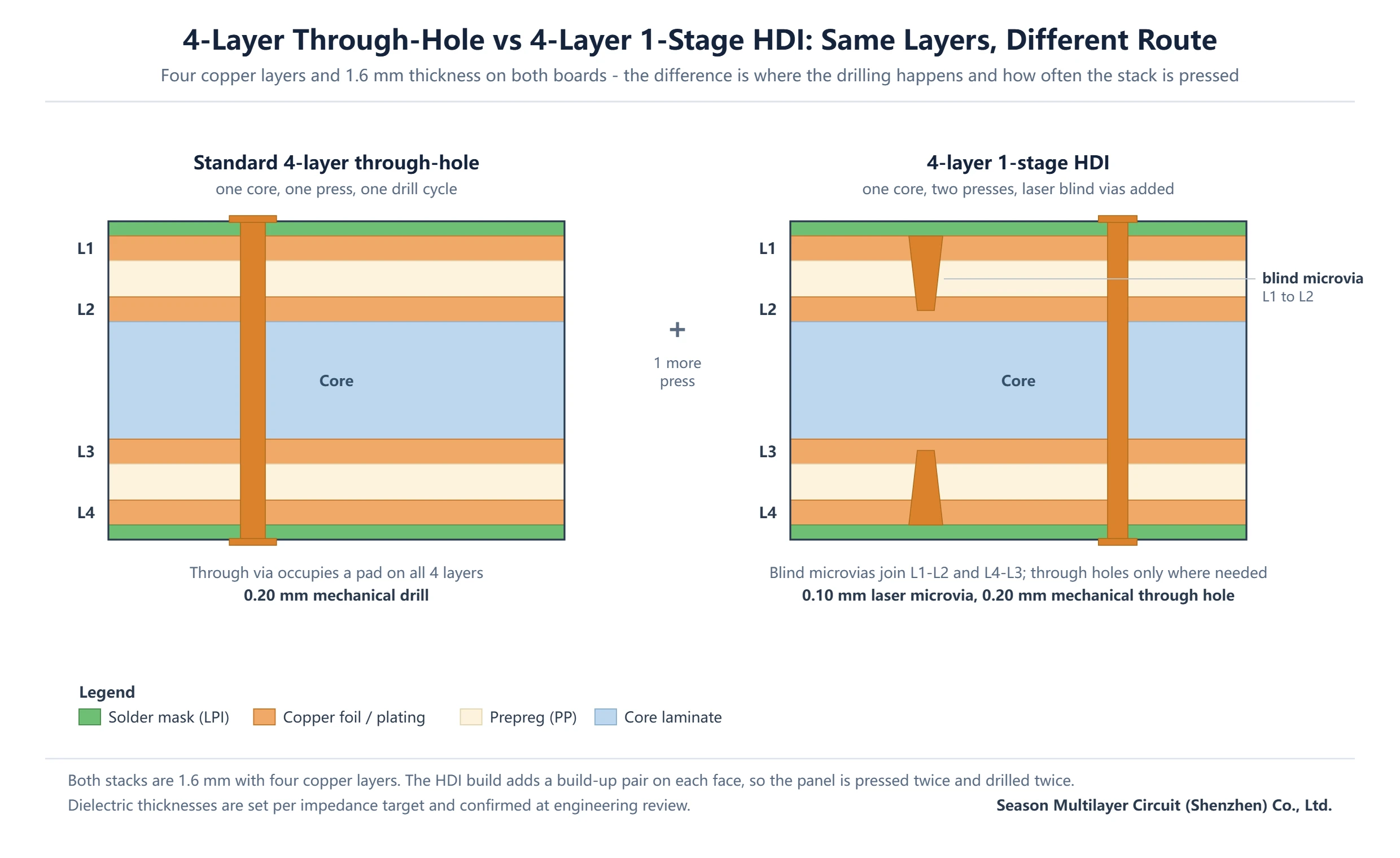
A conventional multilayer board is a stack of copper-clad cores bonded with prepreg in a single press. All drilling happens afterwards and every hole is mechanical, so a via consumes a pad on every layer it passes through, including layers that carry no signal for that net. That is why a through-hole board runs out of routing space long before it runs out of layers.
An HDI board keeps a thin core at the centre and builds dielectric and copper up on the outside. Those outer dielectrics are thin enough to ablate with a laser, so a hole only connects the layers it serves: a blind microvia from L1 to L2, a buried microvia between inner layers, and mechanical through holes only where a connector demands one.
The consequence is that HDI describes a process route rather than a quality tier. A 6-layer board with one core and two lamination cycles is HDI; the same six layers built from two cores in a single press is not, even though the finished thickness is identical. Quotes that compare layer count alone compare two different products.
| Attribute | Standard through-hole multilayer | 1-Stage HDI | 2-Stage HDI |
|---|---|---|---|
| Drilling | Mechanical only | Mechanical + laser (one build-up cycle) | Mechanical + laser (two build-up cycles) |
| Via types in use | Through vias | Through + blind microvias | Through + blind + buried microvias |
| Lamination cycles | 1 | 2 | 3 |
| Cores in the stack | 2 or more | 1 (typical) | 1 (typical) |
| Working minimum trace / space | 3/3 mil | 2.5/2.5 mil | 2/2 mil |
| Minimum via diameter | 0.20 mm mechanical | 0.10 mm laser | 0.10 mm laser (0.076 mm on review) |
| Relative cost index | 1.0 | roughly +30–60% | 1-stage plus 30–100% per extra stage |
| Common layer range | 2–30 | 4–12 | 8–14 |
The cost index is ordinal, not a price list. It moves with layer count, microvia count, panel utilisation and the yield a geometry can hold, so treat it as a way to rank options before a formal quote and expect the final relationship to be confirmed at engineering review.
Cores and Lamination Cycles: Where the Extra Cost Starts
Each additional press is not one more operation but a sequence repeated. Between presses the subassembly is drilled, plated, imaged, etched and inspected, then bonded again with fresh prepreg, and every step has to register to features already on the subassembly. Two presses means two drill programs, two plating runs and two registration budgets stacked together.
The 6-layer comparison shows the mechanism. A standard 6-layer board uses two cores (L2/L3 and L4/L5) and a single press, with copper foil outside. A 6-layer 1-stage HDI uses one core (L3/L4) and builds up L2/L1 on top and L5/L6 below, so it needs two presses. Layer count and finished thickness can be identical; the drill sequence and the price are not.
| Construction | Cores | Lamination cycles | Hole types drilled |
|---|---|---|---|
| 4-layer, through-hole | 1 | 1 | Mechanical through only |
| 4-layer, 1-stage HDI | 1 | 2 | Laser blind + mechanical through |
| 6-layer, through-hole | 2 | 1 | Mechanical through only |
| 6-layer, 1-stage HDI | 1 | 2 | Laser blind + mechanical through |
| 8-layer, 2-stage HDI | 1 | 3 | Laser blind + buried + mechanical through |
| 14-layer, 2-stage HDI (2+10+2) | 1 plus inner subassembly | 3 | Laser blind + buried + mechanical through |
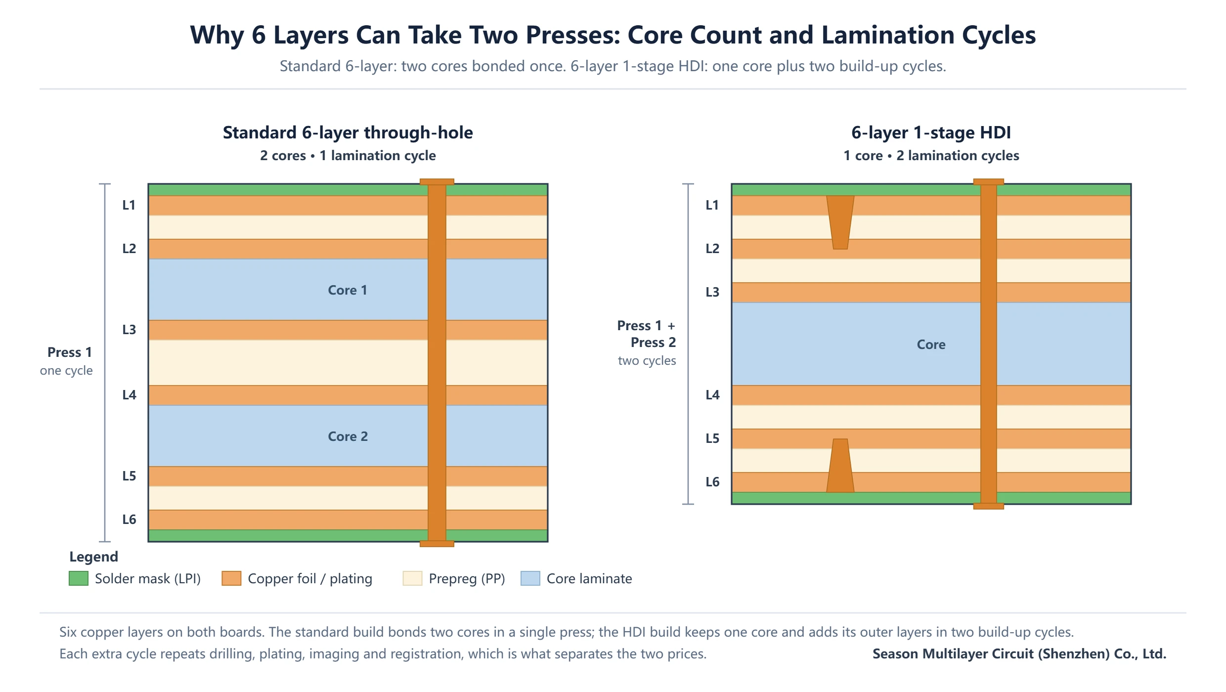
Registration is where the extra cycles bite. Every press contributes a small positional error that has to be absorbed by the annular ring of each via on the layers being bonded, and thin build-up dielectrics leave less room to absorb it. That is why stackup symmetry and copper balance matter more here than on a through-hole board — see the PCB stackup design rules.
Via Geometry: Mechanical Drill vs Laser Microvia
Laser depth is why HDI dielectrics are thin. On the 14-layer 2-stage build described below, the minimum mechanical through hole is 0.20 mm and the minimum laser blind via is 0.10 mm; 0.076 mm is reviewed case by case rather than quoted as standard. The laser ablates dielectric and stops on the copper underneath, so the layer it cuts must be thin and uniform, typically 0.1 mm or less.
Depth-to-diameter ratio is the second limit. A microvia plated at roughly 1:1 fills reliably; add depth without widening the hole and plating thins toward the bottom, which is where barrel cracks start. It is the same plating-throw problem as through-hole aspect ratio, compressed into a 100 µm feature — the aspect ratio guide covers that limit.
What the microvia buys is pad real estate. A 0.10 mm via with a small capture pad occupies a fraction of the area a 0.20 mm through-hole pad needs on every layer, and it can sit inside a BGA pad grid instead of in the channel between pads. That is what makes a 0.4 mm pitch device routable; mechanical vs laser drilling covers the tooling side.
HDI PCB vs Standard PCB: Routing Density and Line Width
Standard multilayer production here runs at 3/3 mil trace and space as a comfortable baseline. HDI moves to 2.5/2.5 mil in routine production and 2/2 mil on volume work, with 1.8/1.8 mil sampled on review. On a 0.5 mm pitch BGA that is not cosmetic: 2/2 mil lets two traces pass between adjacent pads where 3/3 mil allows one, which can halve the signal layers needed to escape.
Pitch is the harder wall. At 0.8 mm and 0.5 mm a through-hole board usually escapes a two-row perimeter with dog-bone vias and 3/3 mil routing. At 0.4 mm the pads are too close for a via between them, so it has to move into the pad, which means a filled and planarised via-in-pad or a microvia landing on the pad below. Below 0.35 mm the escape needs stacked microvias.
The trade moves into the fabrication notes rather than the CAD file. A via-in-pad not specified as filled and capped will wick solder away from the joint during reflow, and a microvia landing off centre by more than its annular ring fails at plating. Via-in-pad design and manufacturing and stacked vs staggered microvias cover both failure modes.
Impedance Control and Signal Integrity Differences
Impedance is the third area where HDI PCB vs standard PCB diverge, and it favours HDI for a physical reason: the build-up dielectric between a signal layer and the plane below is thin. Thin dielectric means a narrow trace reaches 50 Ω single-ended or 90–100 Ω differential, so the target is met with less routing width and the field stays more tightly confined, lowering crosstalk at a given spacing.
Tolerance should be specified rather than assumed. Controlled-impedance nets here are held to ±10% as standard, with ±8% and ±5% available on tighter geometries, measured on a coupon built with the same stack as the panel and read with TDR. The impedance measurement methods article explains why a measured coupon value belongs in a purchase specification.
What HDI does not do is repair a stackup that was never designed for the signalling. If the return path jumps planes under a differential pair, or a reference plane is split beneath a clock, a thinner dielectric will not fix it. Get the stackup right first through the HDI PCB technology guide, then use microvias to recover routing space.
The Relative Cost Ladder for HDI Builds
Cost is where HDI PCB vs standard PCB turns into a commercial decision, and it moves in steps. The first step is the change from through-hole to 1-stage: one extra press, a laser drill program and tighter imaging, which in relative terms adds roughly 30–60%. Each additional stage typically adds another 30–100%, because it repeats the entire build-up sequence on a subassembly that is already expensive.
Yield risk is the second-order effect and often the larger one. A 0.10 mm microvia plated into a 0.1 mm dielectric is a tighter process than a 0.30 mm through hole, and scrap is charged per panel — a panel holding fourteen layers of processed work costs far more to lose than a 4-layer one. That is why quotes for the same nominal geometry diverge between fabricators.
| Cost driver | Why it is charged | How a design can reduce it |
|---|---|---|
| Extra lamination cycle | Full drill, plate, image and register sequence repeated | Stay at 1-stage where the escape allows |
| Laser drill time | Microvia count drives drill program length | Use the largest microvia that still fits the pad |
| Tighter line width | 2/2 mil narrows the imaging process window | Keep 2.5/2.5 mil unless density demands 2/2 |
| Via-in-pad filling | Resin fill and planarisation is a separate step | Use via-in-pad only where pitch forces it |
| Impedance coupon | Coupons must be built with the production stack | Group nets into fewer impedance classes |
| Panel utilisation | Small or odd outlines waste panel area | Review the array before releasing data |
Lead time behaves the same way. An 8–10 layer 2-stage HDI prototype typically runs 17–18 working days from released data, assuming the stackup is frozen; a stackup change mid-build restarts the lamination sequence. Dates are confirmed at engineering review, where drill splits and dielectric thicknesses settle.
When HDI Is Worth the Premium: A Decision Table
Three numbers usually settle HDI PCB vs standard PCB for a given design: the finest BGA pitch, the number of signal layers the escape demands, and whether the board outline can grow. Work outward from the tightest device rather than upward from the layer count.
| Situation | Recommended construction | Reason |
|---|---|---|
| 0.8 mm pitch or coarser, escape fits current layers | Standard through-hole multilayer | Dog-bone vias and 3/3 mil routing are sufficient |
| 0.5 mm pitch, two-row perimeter escape | Standard through-hole, or 1-stage if tight | One trace between pads still works at 3/3 mil |
| 0.5 mm pitch with dense field arrays | 1-stage HDI | Microvias free the channels between pads |
| 0.4 mm pitch, via-in-pad required | 1-stage or 2-stage HDI | Via must move into the pad and be filled |
| 0.35 mm pitch and below | 2-stage or any-layer HDI | Escape needs stacked microvias |
| Outline cannot grow, layer budget used | HDI, scope set by an escape study | Density has to come from the third dimension |
| High volume, cost-sensitive, 0.8 mm pitch | Standard through-hole multilayer | The HDI premium buys nothing at that pitch |
The reverse case deserves equal weight. Stay on a standard board when the finest pitch is 0.8 mm or coarser, when the layout has room for dog-bone vias and 3/3 mil routing, when the product is cost-sensitive at volume, or when thicker copper and mechanical robustness matter more than density. A power board with a low via count rarely gains from build-up layers.
The list that forces HDI is shorter but firmer: a 0.4 mm pitch device, an outline that cannot grow, or a layer budget already at the limit of what the stack can carry. Any one of those three makes the microvia question unavoidable, and the only remaining choice is how many stages it takes.
A DFM Checklist Before You Specify an HDI Build
Most HDI rework we see is a data problem rather than a drilling problem. The board arrives with through-hole vias the designer intended to be blind, or with via-in-pad pads never flagged for filling, and the first article reproduces the data exactly as sent.
- Keep microvias on a separate padstack from through vias; when the CAD tool merges them the fabricator drills both as through holes.
- Confirm the layer pair each microvia connects, because a 1-stage build only reaches L1–L2 and L(n)–L(n-1).
- State whether via-in-pad is resin filled and copper capped or plating filled; the two routes carry different rules.
- Define the solder mask treatment for every via class (tented, plugged or opened) and match it to the assembly method.
- Check stackup symmetry and copper balance before release, since an unbalanced multi-press build warps.
- Put impedance targets, tolerance and coupon requirements in the fabrication notes, not in an email thread.
- Confirm panel size and array so the laser drill program matches the panel that will be drilled.
- Name the acceptance class (IPC Class 2 or Class 3) so inspection criteria are fixed before the first article.
Send the Gerber data with the drill file split by hole type: mechanical through, laser blind and buried. A merged drill file is the most common reason a first article comes back as a through-hole board. Where the design relies on HDI geometry, cite the IPC-2226 sectional design standard so both sides work from the same definitions.
Reference Build: A 14-Layer 2-Stage HDI Specification
A concrete build makes the trade-offs easier to read. This is a production 14-layer 2-stage HDI with a 2+10+2 build on FR-4 with Tg 170, used for high-end video processing and industrial control work where a large BGA array has to escape from a small outline.
| Parameter | Value |
|---|---|
| Layer count / build | 14 layers, 2-stage, 2+10+2 |
| Base laminate | FR-4, Tg 170 |
| Finished thickness | 1.6 mm |
| Outer / inner copper | 1 oz / 0.5 oz |
| Minimum mechanical through hole | 0.20 mm |
| Minimum laser blind via | 0.10 mm |
| Minimum trace / space | 2.5/2.5 mil |
| Minimum BGA pad | 0.20 mm |
| Surface finish | ENIG, 1–2 µin gold |
Two details are worth noticing. Trace and space sits at 2.5/2.5 mil rather than 2/2 mil because the design did not need the extra density, and staying one step off the process limit buys yield. The 0.20 mm minimum BGA pad corresponds to a 0.4 mm pitch array — precisely where through-hole escape stops working. The same construction is available as a 14-layer 2-stage HDI prototype, with a 10-layer 2-stage HDI board or a 4-layer 1-stage HDI panel covering the lower end of the ladder.
Frequently Asked Questions
Is HDI PCB vs standard PCB much more expensive to build?
Yes, but in steps rather than multiples. The first stage of build-up typically adds roughly 30–60% over an equivalent through-hole build, and each additional stage adds another 30–100% because the whole lamination sequence repeats. The premium is bounded by the number of stages the escape actually needs, which is why an escape check should come before a quote.
How do I decide between HDI PCB vs standard PCB for a new design?
Start from the tightest BGA pitch. At 0.8 mm and 0.5 mm a through-hole board usually escapes with dog-bone vias and 3/3 mil routing. At 0.4 mm the via no longer fits between pads and has to move into the pad, which means microvias. If the outline cannot grow and the layer budget is used up, the same conclusion arrives from the other direction.
Can a standard multilayer board have blind and buried vias?
Only in a limited way. A buried via has to be drilled before the layers above and below are bonded, which requires more than one lamination cycle, and a board with more than one cycle is by definition a build-up construction. A single-press through-hole board can only carry through vias that pass through every layer.
What is the smallest laser microvia a fabricator can drill?
On this site’s production builds, 0.10 mm is the standard laser blind via and 0.076 mm is reviewed case by case rather than quoted as routine. The limit is set by the dielectric thickness the laser has to stop through and by the plating aspect ratio of the finished hole, so the answer is tied to a specific stackup rather than to the drill alone.
Does HDI always require via-in-pad?
No. Via-in-pad is only needed when a via has to sit inside a surface-mount pad, typically for 0.4 mm pitch arrays or fine-pitch QFN thermal pads. Blind microvias placed in the channel between pads are enough for many 0.5 mm designs, and those need neither filling nor capping, which keeps cost and assembly risk lower.
How many lamination cycles does a 2-stage HDI board need?
Three. The subassembly is pressed once to form the inner core, then the first build-up pair is laminated on both faces, then the second pair is added. That is why 2-stage pricing steps up rather than scaling smoothly: each cycle repeats drilling, plating, imaging and registration on work that has already accumulated value.
Which layer counts can be built as 2-stage HDI?
Eight to fourteen layers covers most 2-stage work, including asymmetric builds such as 2+10+2. Below eight layers a 1-stage build usually has enough routing space, and above fourteen the stack generally moves to 3-stage or any-layer. The deciding factor is the escape requirement, not the layer count on its own.
Have Your Stackup Reviewed Before You Commit to HDI
Whether HDI PCB vs standard PCB is the right call depends on data that usually looks final at the quotation stage. Send the Gerber set, the layer assignment and the pitch of the tightest device, and the engineering team will come back with the construction that meets it, with the drill split, the stackup and the impedance requirement written down.
If a 1-stage build covers the escape, that is the answer you will get. Start with the PCB manufacturing services overview or the HDI technology guide for the process detail behind these numbers.