Book Appointment Now

The SMT assembly process runs from stencil printing to reflow and test. See the controls at each stage, the defects they prevent and the limits held in production.
SMT Assembly Process: Stencil, Placement and Reflow Explained
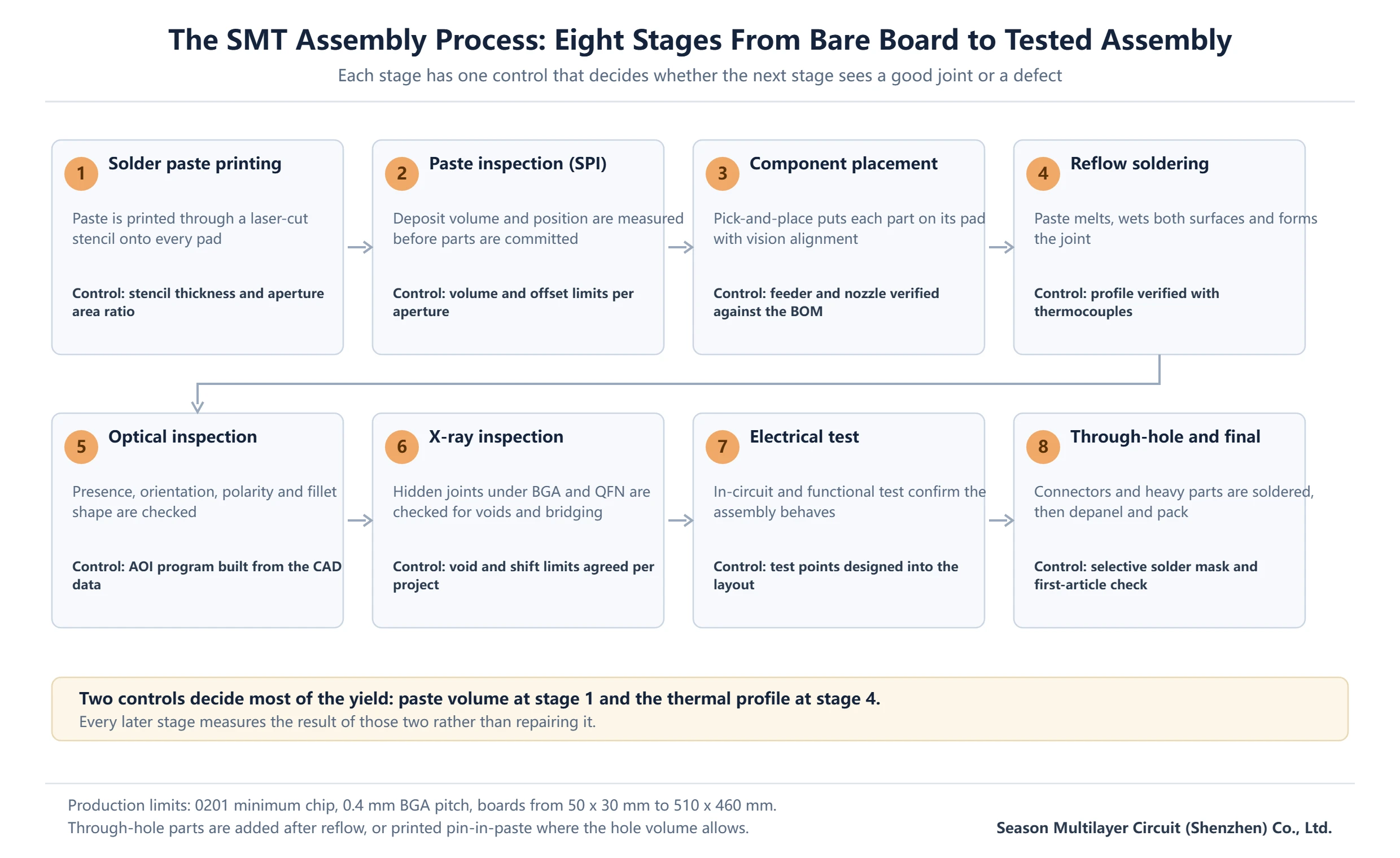
The SMT assembly process is where a finished bare board either becomes a working assembly or becomes a rework ticket, and most of that outcome is decided before the first component is placed. Paste volume, stencil aperture design, placement force and the reflow profile interact, so a change made to clear one defect routinely creates another further down the line.
This walkthrough follows a panel through the line: stencil and paste printing, placement, reflow, inspection and test, then the through-hole operations that mixed-technology assemblies still need. Each stage is paired with the defects it causes and the control that prevents them, and the capability limits quoted are the ones held in production here.
Table of Contents
- What the SMT Assembly Process Covers
- Stencil Design and Solder Paste Printing
- Component Placement and Accuracy Limits
- Reflow Profile: Four Zones and What They Control
- Inspection and Test After Reflow
- Adding Through-Hole Parts to an SMT Build
- How the SMT Assembly Process Affects Cost and Lead Time
- DFM Rules That Prevent Rework
- What to Send for an Assembly Review
- FAQ
- Send the Gerber and BOM for an Assembly Review
What the SMT Assembly Process Covers
Surface mount technology places components on pads on the surface of the board and joins them with solder paste that is reflowed in an oven. No lead passes through the board, so the only holes left on an SMT side are vias and the occasional through-hole part added later. That single change is what removed the board-area penalty that through-hole assembly carried for every component pin.
The process is wider than placement. A full run covers stencil printing and paste inspection, placement, reflow, automated optical inspection, X-ray where joints are hidden, electrical test, then the secondary operations: through-hole insertion and soldering, depanelisation, cleaning where the flux demands it, and conformal coating when the application calls for it.
| Attribute | SMT assembly | Through-hole assembly |
|---|---|---|
| Component mounting | On pads, board surface | Leads through drilled holes |
| Joint formation | Solder paste reflowed in an oven | Wave, selective or hand soldering |
| Board area per part | Smallest, no lead holes needed | Larger, every lead needs a hole |
| Typical smallest part | 0201 chip | Leaded discrete, pitch limited |
| Rework method | Hot air or IR with local stencil | Desoldering tool and iron |
| Joint strength | Good in shear, weaker in peel | Strong against pull-out |
| Best fit | Dense digital and mixed-signal boards | Connectors, transformers, high-vibration parts |
Most production boards are mixed technology rather than pure SMT. The order of operations then matters: the SMT side with the higher component count is usually placed and reflowed first, because the through-hole parts and connectors that follow are taller and would obstruct the stencil and the placement head.
Stencil Design and Solder Paste Printing
The stencil is a laser-cut stainless foil tensioned on a frame, and its thickness sets the paste volume delivered to every aperture. Typical foils run from 0.10 mm for fine-pitch work to 0.15 mm for boards dominated by larger parts. The governing ratio is the aperture area divided by the area of the aperture walls: below roughly 0.66, paste tends to stay in the hole instead of releasing onto the pad. This is the first place where the SMT assembly process loses yield, and no amount of placement accuracy recovers it.
Print quality is a machine and material problem at once. Squeegee pressure, angle and speed, separation speed, stencil tension, paste viscosity and age, room temperature and humidity all move the deposit. So does the pad finish: an ENIG pad releases paste more predictably than a rougher HASL surface, which is one reason finish choice appears in assembly discussions as well as fabrication ones — see the surface finish comparison.
Three print defects account for most downstream fallout. Insufficient deposit leaves opens that only appear after reflow; excess deposit bridges adjacent pads or forms solder balls; a deposit that slumps before placement lifts one end of a small chip during reflow and produces tombstoning. Solder paste inspection after the printer catches all three before the parts are committed.
Component Placement and Accuracy Limits
Placement capability on this line is 0201 chip components as the smallest part, BGA at 0.4 mm pitch with a 0.20 mm minimum pad, and the usual package families: SOP, SOT, QFN, QFP and BGA. Board size runs from 50 × 30 mm up to 510 × 460 mm, which sets how the array has to be laid out before placement is even considered.
| Capability | Production limit |
|---|---|
| Smallest chip component | 0201 |
| Minimum BGA pitch | 0.4 mm |
| Minimum BGA pad | 0.20 mm |
| Package families | SOP, SOT, QFN, QFP, BGA |
| Maximum board size | 510 × 460 mm |
| Minimum board size | 50 × 30 mm |
| Placement reference | Vision alignment on global fiducials |
| Typical inspection | AOI on all boards, X-ray on hidden joints |
Accuracy is not only the machine specification. Vision alignment needs fiducials that the camera can distinguish from copper, nozzles have to match the part, and feeder setup has to be verified against the BOM before the first board. Moisture sensitivity matters just as much: a package that has absorbed moisture and is not baked before reflow can delaminate or crack as the water turns to steam.
The defects that survive to inspection usually come from small offsets rather than gross errors: a part rotated by one 90° step because the centroid file used a different rotation convention, a BGA shifted by half a pad, or a chip standing on one end because the two pads received unequal paste. That is the part of the SMT assembly process a data review can fix for free.
Reflow Profile: Four Zones and What They Control
Reflow is the stage where the SMT assembly process either makes a joint or makes a defect, and the oven is profiled in four stages. Preheat brings the assembly up without thermal shock, soak lets the flux activate and the whole board reach a uniform temperature, reflow takes the alloy above its liquidus so the powder coalesces and wets the pads, and cooling solidifies the joint with a grain structure that survives thermal cycling.
For a lead-free SAC305 alloy the working window is a peak of roughly 235–245 °C, 45–90 seconds above the 217 °C liquidus, and a ramp no steeper than 2–3 °C per second. Those figures are a starting window, not a recipe: the paste supplier’s datasheet governs, and the profile is verified with thermocouples on a representative panel that carries the same copper distribution and the same large thermal masses as production.
| Zone | Purpose | If the window is missed |
|---|---|---|
| Preheat | Ramp the assembly without thermal shock | Splatter, paste slump, component cracking |
| Soak | Flux activation and thermal equalisation | Incomplete activation, uneven wetting |
| Reflow | Alloy melts and wets both surfaces | Cold joints, non-wetting, head-in-pillow |
| Cooling | Controlled solidification of the joint | Grain coarsening, fillet cracking, warpage |
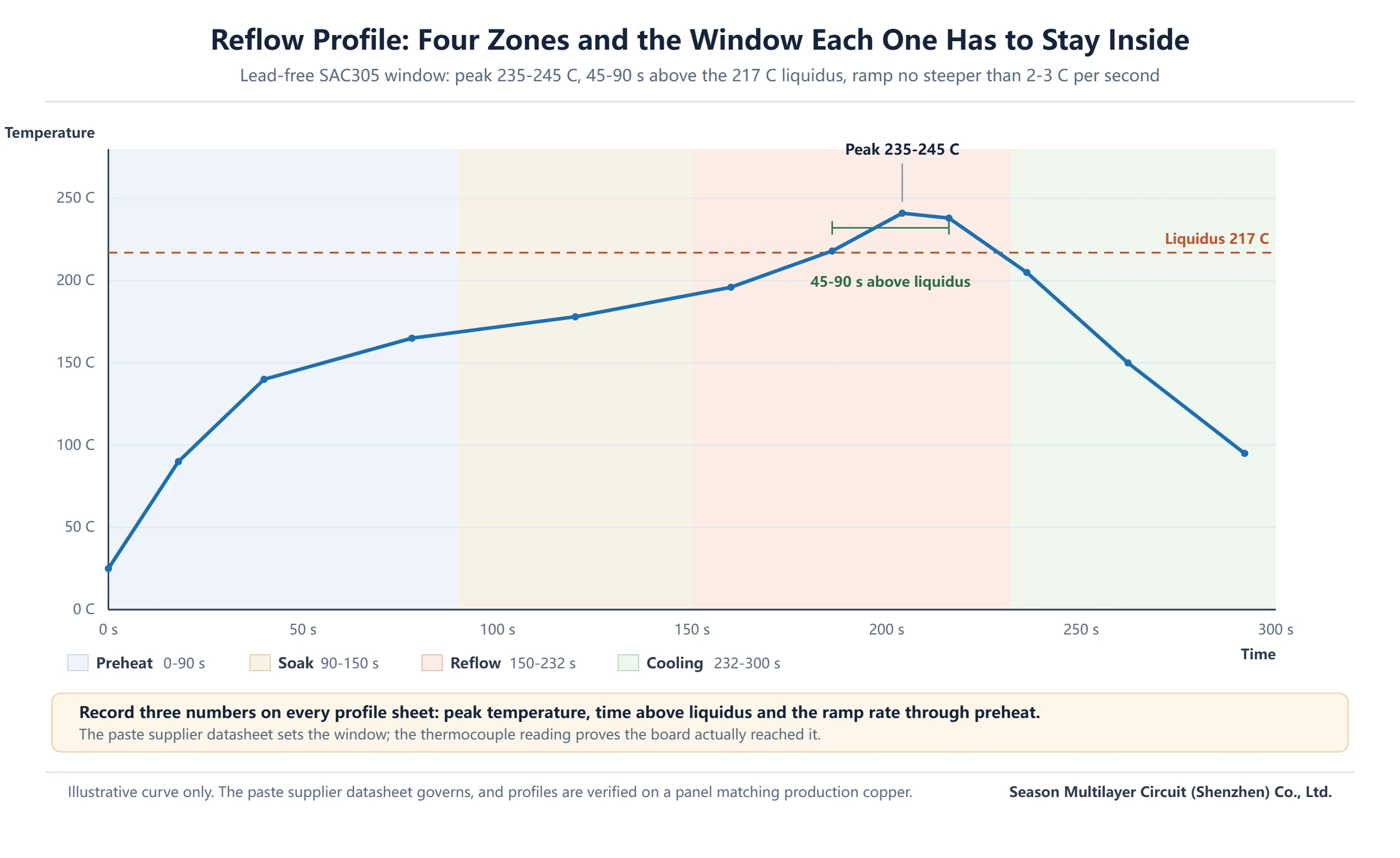
Two complications are worth planning for. Double-sided assemblies go through the oven twice, so the second pass must not remelt the first side — either the bottom side carries small parts held by surface tension, or the profile is trimmed and the carrier supports the board. Large boards and heavy copper planes also absorb heat unevenly, which is why stackup balance is an assembly concern and not only a fabrication one.
Inspection and Test After Reflow
Inspection is layered because the SMT assembly process can fail in ways no single method sees. Paste inspection checks the deposit before placement. Optical inspection after reflow checks presence, orientation, polarity and fillet shape from above. X-ray looks through the package at joints that no camera can reach. In-circuit and functional test then check the electrical behaviour of the finished assembly.
The split matters for expectations. Optical inspection sees a QFN fillet on the perimeter but not the thermal pad underneath, and it cannot judge a BGA joint at all — that is X-ray work, where voiding and head-in-pillow show up as density differences. In-circuit test needs accessible test points, so a design that only offers fine-pitch pads under a shield will be limited to functional test or boundary scan.
Acceptance criteria should be named in the purchase order rather than argued at delivery. Assemblies are judged against the IPC-A-610 acceptability standard, with Class 2 as the normal commercial target and Class 3 where continuity of service matters. The Class 3 requirements article explains how those classes differ on the bare board side.
Adding Through-Hole Parts to an SMT Build
Connectors, transformers, relays and anything that has to survive mechanical pull-out stay through-hole, so most assemblies are mixed and the SMT assembly process handles only part of the component count. After the SMT side is reflowed, the through-hole parts are inserted and soldered by selective soldering, wave soldering with a mask, or hand soldering where the volume or the geometry justifies it.
Pin-in-paste is the alternative worth knowing: the through-hole pads are printed with paste and the part is placed before reflow, removing a secondary operation entirely. It works well for small pin counts and short pins, and it runs into trouble when the hole volume exceeds what a stencil can deposit, which is why hole diameter and pin length have to be checked before the design is committed to it.
The mechanical details decide whether the mixed build reflows cleanly. Tall parts placed before the second reflow obstruct the placement head, masking for wave solder has to keep solder out of adjacent SMT pads, and connector coplanarity has to hold after both thermal cycles. Those are the points a first-article inspection is really testing.
How the SMT Assembly Process Affects Cost and Lead Time
Assembly cost tracks complexity rather than board area. The drivers are the number of unique part numbers, the total placement count, whether the board is single or double sided, how fine the finest pitch is, how many stencils are needed, and how much test coverage the product requires.
A few of those drivers scale in steps. A second reflow pass adds oven time, a second placement program and a second inspection cycle. Fine-pitch and BGA content pushes inspection from sampling to full coverage, and X-ray is charged per panel. A board with thirty unique parts and a board with three hundred differ far more in setup and feeder time than in the number of components placed.
| Cost driver | Why it adds work | How to reduce it |
|---|---|---|
| Unique part numbers | Feeder setup and verification per line change | Consolidate values and packages |
| Placement count | Machine time scales with placements | Accept slightly larger packages where space allows |
| Double-sided assembly | Second print, second reflow, second inspection | Keep the dense side single-sided where possible |
| Fine pitch and BGA | Full X-ray and slower placement | Reserve fine pitch for the devices that need it |
| Test coverage | Fixture, program and test time | Provide test points and a test specification |
| Tooling | Stencil, carrier, fixture per revision | Freeze the layout before tooling is ordered |
Lead time is usually set by what arrives before the line, not by the line itself. The bare board has to be finished and inspected first, and component sourcing frequently dominates the schedule — a single long-lead IC can hold an entire assembly. Dates are confirmed once the BOM is verified and the bare boards are in hand, which is why the prototype build sequence is quoted as a chain rather than a single step.
DFM Rules That Prevent Rework
Most assembly rework traces back to a layout decision that looked harmless in CAD, not to the SMT assembly process itself. These are the checks worth running before the data package is released:
- Leave enough solder mask dam between adjacent pads; a dam that breaks during printing causes bridging that no profile change will fix.
- Keep pad-to-pad clearance above the assembly limit for the package you chose, not just above the bare-board limit.
- Design 0201 and 0402 land patterns to equalise paste volume on both terminals, or tombstoning becomes a yield issue.
- Place fiducials diagonally, clear of copper and mask, and keep at least three globally visible ones on each side.
- Keep tall parts away from the edge the placement head approaches, and off the side that faces down in the second reflow.
- Add test points on nets that need in-circuit coverage rather than relying on probing component pads.
- Keep component courtyards honest so the placement program does not collide with neighbouring parts.
- Confirm polarity marking is visible after assembly, not hidden under the part or lost under the mask.
One more check sits outside the layout. Confirm that the paste layer in the Gerber data matches the stencil you intend to order — a paste layer copied from an older revision is a common reason a first article prints badly while the bare boards are perfect.
What to Send for an Assembly Review
An assembly quote is only as good as the data behind it. The package that avoids a round of questions contains the BOM with manufacturer part numbers and approved alternates, the Gerber set including paste layers, a centroid file with units and rotation convention stated, an assembly drawing showing polarity and any parts that must not be substituted, and the test requirement.
The gaps that cause most delay are predictable: a centroid file in mils when the placement program expects millimetres, no alternates listed for a part with a long lead time, missing polarity marks for diodes and electrolytics, and no statement of which side is the primary assembly side. Each of those is a two-minute fix on the customer side and a day of email on ours.
Frequently Asked Questions
What is the SMT assembly process in simple terms?
It is the sequence that joins surface-mount components to a bare board. Solder paste is printed through a stencil onto the pads, components are placed by machine, and the whole assembly passes through a reflow oven where the paste melts and forms the joints. Inspection and electrical test follow, then any through-hole parts are added.
What is the difference between SMT and through-hole assembly?
Through-hole parts have leads that pass through drilled holes and are soldered on the far side, which costs board area for every pin. SMT parts sit on pads on the surface and are joined by reflowed paste, so no holes are needed. SMT is denser and cheaper to automate; through-hole joints resist pull-out better and remain standard for connectors and heavy parts.
What is the smallest component you can place?
0201 chip components are the production limit on this line, with BGA devices down to 0.4 mm pitch and 0.20 mm pad diameter. Anything finer needs a dedicated fine-pitch line and a stencil and paste combination built around it, so it is quoted after a review of the actual land pattern rather than assumed.
Do you inspect every joint on an SMT assembly?
Every board passes optical inspection, which covers presence, orientation, polarity and visible fillets. Joints hidden under a package are the exception: BGA and QFN thermal pads are checked by X-ray, and the coverage level is agreed per project because X-ray time is charged per panel. Electrical test adds functional coverage where test points allow it.
Why do BGA joints need X-ray inspection?
The joints sit under the package body, so no camera can see them. X-ray transmission shows the solder mass of each ball, which reveals bridging, missing balls, excessive voiding and head-in-pillow defects where the ball and the paste never fully coalesced. Optical inspection can confirm the package is present and aligned, but not that the joints formed.
Can SMT and through-hole parts be assembled on one board?
Yes, and most boards are built that way. The SMT side is printed, placed and reflowed first, then through-hole parts are inserted and soldered by selective or wave soldering, or by hand. Pin-in-paste can eliminate that second operation for small pin counts by printing the holes along with the pads.
What data do I need for an SMT assembly quote?
A BOM with manufacturer part numbers and approved alternates, the Gerber set including paste layers, a centroid file stating units and rotation convention, an assembly drawing with polarity and no-substitution notes, and the test requirement. Missing alternates or a centroid in the wrong units are the two most common reasons a quote stalls.
Send the Gerber and BOM for an Assembly Review
Assembly questions are usually answered faster from the data than from a description. Send the Gerber set, the BOM and the centroid file, and the review will come back with the stencil thickness, the placement and inspection plan, and the points in the layout that would cause rework if they were left as they are.
Bare boards and assembly can be quoted together so the stackup, the surface finish and the paste layer are decided in one pass. Start with the PCB manufacturing services overview or the PCBA supplier checklist before the first build.