Book Appointment Now

The PCB manufacturing process explained stage by stage, from panel cutting to final inspection, so you know what happens to your boards and why it matters.
PCB Manufacturing Process: From Panel Cutting to Final Shipment
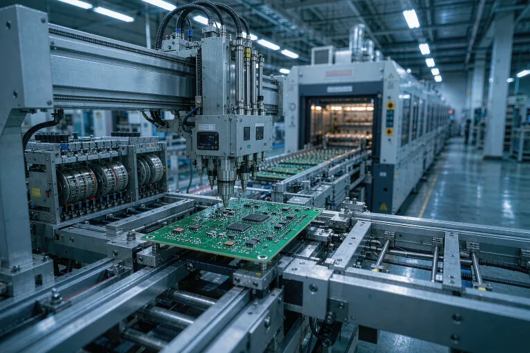
When you hand a fab your Gerber files, roughly two weeks of industrial chemistry, precision machining and inspection stand between the data and the boards that arrive at your dock. Most hardware teams know the outputs of the PCB manufacturing process intimately — they test the boards, assemble them, ship products built on them — but the sequence of steps inside the factory is often a black box. That is an expensive blind spot: many field failures and quote disputes trace directly back to a misunderstanding of what a given process step can and cannot control.
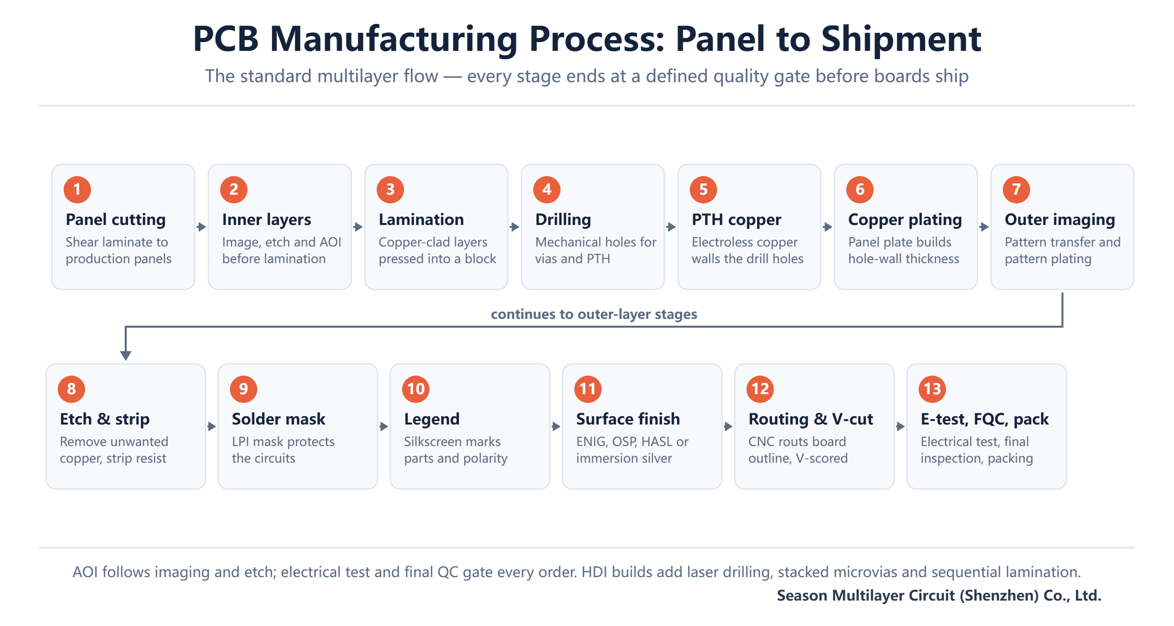
This guide walks the full multilayer flow in order — panel cutting, inner-layer imaging, lamination, drilling, hole metallization, plating, pattern transfer, etching, solder mask, legend, surface finish, machining, and the test-and-inspection chain that gates shipment. Along the way it flags where quality is actually won or lost, and links deeper explainers for each stage if you want the process-level detail.
Table of Contents
- The PCB Manufacturing Process at a Glance
- Engineering Review and CAM: What Happens to Your Gerbers
- Panel Cutting and Preparation
- Inner Layers and Lamination
- Drilling and Hole Metallization
- Pattern Transfer, Plating and Etching
- Solder Mask, Legend and Surface Finish
- Routing, V-Cut and Final Machining
- Electrical Test and Final Inspection
- How the PCB Manufacturing Process Affects Lead Time
- FAQ
- See How Your Build Moves Through Our Floor
The PCB Manufacturing Process at a Glance
A production order does not move through the factory as one continuous operation. It moves as a chain of stage groups, each with its own equipment set, process parameters and quality gate. The table below groups the thirteen production steps into the six blocks a buyer will recognize on any traveler or QC report.
| Stage group | Steps included | What it delivers |
|---|---|---|
| Panel preparation | 1. Panel cutting | Production-size panels from raw laminate |
| Inner-layer formation | 2. Inner-layer imaging and etch | Patterned inner cores, verified by AOI |
| Stack bonding | 3. Lamination | A bonded multilayer block with registered layers |
| Via formation | 4. Drilling · 5. Hole metallization · 6. Copper plating | Conductive through-holes with plated walls |
| Outer-layer formation | 7. Outer imaging · 8. Etch and strip | Finished outer circuits |
| Finishing and shipment | 9–13. Solder mask, legend, surface finish, routing, test and pack | Boards ready for assembly |
Two things are worth noticing before we walk the chain. First, the sequence is additive in risk: an error created at inner-layer imaging becomes invisible once layers are laminated, which is why AOI sits immediately after patterning rather than at final inspection. Second, most lead time is queueing between stages, not the chemistry itself — which is why a fab’s scheduling discipline matters as much as its equipment list.
Engineering Review and CAM: What Happens to Your Gerbers
Strictly speaking, production starts before any laminate is cut. Your manufacturing data passes through engineering review and CAM preparation: the fab checks stackup against capability, validates drill and netlist data, and panelizes your designs to maximize material use while preserving tooling margins. Errors caught here cost a phone call; the same errors caught after lamination cost a rebuild.
This is also where your data format matters more than most buyers expect. Gerber remains the universal interchange format for the imaging steps, and clean, complete Gerber plus an accurate drill file is the single biggest input to a smooth run. The format itself is maintained by its originator — the Gerber specification is published and versioned publicly. If you want to see how the pre-production journey works end to end, our prototyping process guide covers it from file submission to first article.
Panel Cutting and Preparation
The first physical step is cutting: full-size laminate sheets — copper-clad core material — are sheared into production panels sized to the product’s nesting layout. The panel size is not arbitrary; it comes from the CAM stage, which balances unit count against the margins needed for tooling holes, test coupons and the processing rails that grippers and transport systems hold onto.
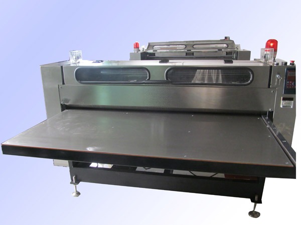
Cutting also sets up edge quality for everything downstream: burrs left by a worn shear blade become registration hazards at drilling and handling damage risks through wet processes. A disciplined line cuts, deburrs and rounds panel corners before the panel ever enters a transport cassette. For the sizing logic — units versus set panels versus working panels — see our panel cutting and sizing explainer.
Inner Layers and Lamination
On a multilayer board, the inner layers are fully formed before bonding. Each core is cleaned, coated with dry-film photoresist, exposed through artwork, developed and etched — leaving the copper pattern that will live inside the finished board. Automated optical inspection then compares every inner layer against the design data; this is the last moment a inner-layer defect is cheap to catch, because after lamination the layer is buried.
Lamination bonds the stack: inner cores, prepreg sheets and outer copper foils are stacked in a press under controlled temperature, pressure and vacuum. The prepreg melts, flows and cures, locking the layers into a single registered block with defined dielectric thicknesses. Squeeze-out, resin flow and layer shift are the parameters to police here — they set the foundation for drilling accuracy and controlled impedance. The mechanics are detailed in our lamination process guide, and the symmetry principles that keep the finished board flat in our balanced stackup guide.
Drilling and Hole Metallization
Drilling creates the holes — plated through-holes for interlayer connection, tooling holes for registration. CNC drilling machines position each panel to micron-level accuracy and hold tight controls on hole diameter, pitch and positional tolerance, because every subsequent layer-to-layer connection depends on these holes landing where the design says. HDI builds add laser drilling for microvias below the mechanical drill’s practical floor — our mechanical vs laser drilling guide covers where each technology wins.
A freshly drilled hole, however, is just bare laminate — non-conductive between layers. Hole metallization changes that. In electroless copper deposition, the panel passes through conditioning, activation and copper baths so that a thin conductive copper layer forms chemically on the hole walls. It is one of the most sensitive steps in the entire flow: a void in the plating of a hole wall is a hidden open circuit that no amount of final inspection will reliably find. The chemistry is covered in our electroless copper (PTH) process guide.
Panel plating then thickens that thin flash to a robust copper thickness across the whole panel, building the hole-wall cross-section that carries current and survives thermal cycling. Copper plating parameters — current density, bath concentration, dwell time — directly set hole-wall thickness uniformity, which is why plating data is a standard ask in any fab audit.
Pattern Transfer, Plating and Etching
Outer-layer formation reuses the imaging chemistry of the inner layers, with one strategic inversion. The panel is coated with photoresist and exposed with the outer artwork; where the pattern develops, the subsequent pattern plating builds up copper — and often a tin etch resist — on the traces that will remain. The plating here is selective: it strengthens conductors and via knees where current density concentrates.
Etching then removes all copper not protected by the plating or resist, and stripping removes the resist, leaving the finished outer circuits. The polarity logic — which artwork is clear and which is opaque, and why electroless copper before imaging makes the classic positive-film flow work — is easy to tangle; our positive vs negative film guide untangles it step by step. Line-width control in this chain is what your impedance spec ultimately leans on, which is why AOI follows immediately.
Solder Mask, Legend and Surface Finish
With circuits complete, the protective layers go on. Liquid photoimageable solder mask is printed, pre-cured, exposed and developed to open windows over pads, then thermally cured. Its job is functional, not cosmetic: it prevents solder bridging during assembly and protects the copper underneath from the environment. Silkscreen legend follows, printing component references, polarity marks and identifiers that assembly and service teams rely on.
Surface finish is the last chemistry the copper sees before packing, and it exists because bare copper oxidizes and will not solder reliably. The common options differ in flatness, shelf life and cost positioning.
| Surface finish | What it is | Typically chosen for |
|---|---|---|
| HASL | Hot-air solder leveling — molten solder coat, leveled | Cost-sensitive boards, through-hole heavy assemblies |
| OSP | Organic solderability preservative — thin organic film | Flat pads, fine pitch, short shelf-life acceptance |
| ENIG | Electroless nickel, immersion gold | Flat, solderable, long shelf life; fine-pitch and backplane work |
| Immersion silver | Thin silver deposit over copper | Flat and solderable with good RF performance |
| Immersion tin | Thin tin deposit over copper | Flat finish for press-fit and backplane applications |
The trade-offs among nickel/gold systems are covered in depth in our ENEPIG surface finish guide. Note that solder mask color and finish choice are independent decisions — color is a customer specification, while the finish is driven by assembly process and reliability requirements.
Routing, V-Cut and Final Machining
Up to this point your boards have lived as one large panel — that is how the factory keeps hundreds of units in register through wet processes. Machining separates them. CNC routing mills the board outline and internal slots per the engineering profile; V-cut scoring cuts a shallow V-groove across the panel so rectangular boards can be snapped apart cleanly at assembly. Countersinks, edge chamfers and depth-controlled routing features are added in the same operation.
Machining quality is deceptively critical. Rough router bites create glass fibers protruding from board edges — a latent insulation risk in humid environments — and poor V-cut depth either cracks prematurely or refuses to separate. This is also where any non-plated mechanical features (mounting holes, fiducial clearances) receive their final dimensions. When the panel design is tight, review routing vs V-cut trade-offs with the fab before panelization is locked, not after.
Electrical Test and Final Inspection
The last stage group proves the boards before they ship. Electrical test — flying probe for prototypes and low volume, fixture-based bed-of-nails grids for volume — checks every net against the design netlist for opens and shorts. It is a netlist-driven test, meaning it verifies continuity and isolation exactly as designed, independent of appearance.
| Checkpoint | Method | What it catches |
|---|---|---|
| Inner and outer AOI | Automated optical comparison to design data | Open/short copper defects, width violations, registration errors |
| Electrical test | Flying probe or bed-of-nails netlist test | Opens and shorts, including latent hole-wall voids exposed by thermal stress |
| FQC — final quality control | 100% visual and dimensional inspection | Surface defects, mask and legend flaws, machining burrs, thickness |
| QA — sampling audit | AQL sampling against acceptance level | Batch-level drift that unit inspection might smooth over |
Visual acceptance criteria are not a matter of taste — they trace to the IPC-A-600 acceptance standard, and the class you specify (Class 2 vs Class 3) changes what is acceptable. Our IPC-A-600 Class 3 guide details the stricter criteria. Packaging closes the process: boards are vacuum-sealed with desiccant, labeled with batch identity, and packed to survive transit — the details that matter if your boards will sit in storage before assembly.
How the PCB Manufacturing Process Affects Lead Time
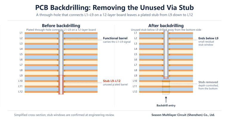
Lead time is the sum of the chain plus the queues between stages, so the factors that move it are predictable. Layer count adds lamination and drilling cycles; controlled impedance adds engineering setup and coupon testing; special processes such as backdrilling, heavy copper or HDI sequential lamination each insert a dedicated stage with its own inspection gate. Surface finish and legend add curing time at the end of the chain.
For a buyer, two practices reliably shorten the timeline without touching quality. First, submit complete and consistent data — stackup intent, impedance targets, and profile drawings included — so engineering review does not bounce the order for clarification. Second, declare special processes up front: a backdrill requirement that surfaces mid-quote reopens the stackup conversation, while one declared in the fab notes is priced and scheduled in a single pass. For complex builds, expect the fab to quote an engineering-review-confirmed window — an 8–10 layer 2-stage HDI prototype, for example, typically runs on the order of 17–18 working days.
Finally, remember that the PCB manufacturing process ends at packing, not at the fab door — how boards are stored and handled on your side determines how much of that factory discipline survives to assembly. Following the IPC handling and packaging recommendations from the Global Electronics Association protects the investment the process has already made.
Frequently Asked Questions
What are the main steps in the PCB manufacturing process?
The standard multilayer flow runs: panel cutting, inner-layer imaging and etch, lamination, drilling, electroless copper (hole metallization), copper plating, outer pattern transfer, pattern plating, etch and strip, solder mask, legend, surface finish, routing and V-cut, electrical test, final QC, then packing and shipment.
How does a multilayer build differ from a double-sided board?
A double-sided board images, etches and masks its two layers directly. A multilayer board first patterns and AOI-verifies inner cores, laminates them with prepreg into a bonded block, and only then drills and processes the outer layers — adding lamination, registration and inner-layer inspection steps that double-sided production does not need.
Why is hole metallization so critical?
Drilled holes are non-conductive laminate; electroless copper chemically deposits a conductive layer on the hole walls, making interlayer connection possible. It happens before any visual pattern exists on the outer layers, and a void in the hole wall is a hidden open circuit that final inspection cannot reliably catch — so bath control and micro-section sampling carry the burden.
What is the difference between FQC and QA sampling?
FQC (final quality control) inspects every board — appearance, dimensions, mask and legend quality — against the acceptance criteria. QA then draws a statistical sample from the passed batch to verify batch-level stability. FQC protects the individual board; QA protects you from process drift across the order.
Which surface finish should I choose?
Match the finish to assembly and storage needs: ENIG for flat, fine-pitch, long-shelf-life boards; OSP for flat pads when boards assemble quickly; HASL for cost-driven, through-hole-heavy assemblies; immersion silver or tin where flatness and solderability must coexist with specific RF or press-fit requirements.
How long does the PCB manufacturing process take?
It depends on layer count and special processes. Simple double-sided and 4-layer prototypes move in days; complex HDI builds such as an 8–10 layer 2-stage prototype typically run on the order of 17–18 working days. Any committed lead time should be confirmed at engineering review, where special processes are scoped.
What files does a fab need to start production?
Gerber data for every copper, mask and legend layer, an accurate NC drill file, a fabrication drawing with stackup and controlled-impedance targets, and the board profile. Complete, self-consistent data shortens engineering review — the stage where most delays and misquotes originate.
See How Your Build Moves Through Our Floor
Every order that enters our plant follows the chain described above — with AOI after imaging, netlist-based electrical test, and engineering review before the first panel is cut. If you want your next build scheduled against a real process flow rather than a generic promise, start from our PCB manufacturing services page and send your Gerber files with the stackup notes.
For multilayer and HDI builds, our team will confirm process feasibility, impedance scope and lead time in one review pass — before production begins. You can also browse a completed 12-layer high-speed backplane build to see the output of this process on a demanding application.