Book Appointment Now

Black hole vs electroless copper: how the two hole metallization routes differ in chemistry, throughput and design limits, with a selection table for buyers.
Black Hole vs Electroless Copper: PCB Hole Metallization Compared
Two boards can leave the same drill room and still behave completely differently in the field, because what happens next — hole metallization — decides whether every via in the stack becomes a reliable conductor or a latent defect. Buyers comparing quotes rarely see this step on the quotation sheet, yet the choice between black hole vs electroless copper changes the chemistry load, the cycle time, and the design envelope a fabricator can hold.
This guide explains both routes the way a process engineer would: what each seed layer actually is, where the process chain is longer or shorter, which aspect ratios and layer counts each one is comfortable with, and how to judge the trade-offs at engineering review rather than on a brochure page.
Table of Contents
- Why the Hole-Wall Seed Decides Barrel Reliability
- Electroless Copper Plating: The Classical Seed
- Carbon Direct Metallization: The Condensed Chain
- Black Hole vs Electroless Copper: Side-by-Side Comparison
- Aspect Ratio and HDI: Where the Limits Sit
- Signal Integrity and Reliability Notes
- Cost and Environmental Trade-Offs
- Choosing Black Hole vs Electroless Copper for Your Build
- What to Confirm at Engineering Review
- FAQ
- Have Your Stackup and Hole Sizes Reviewed Before Release
Why the Hole-Wall Seed Decides Barrel Reliability
A mechanically drilled hole passes through glass fibres, resin and copper foils, and the wall it leaves behind is an insulator. Nothing conducts until a thin seed layer is created on that wall, and only then can copper electroplating build the barrel that carries current between layers. If the seed is incomplete, the barrel inherits the flaw no matter how well the plating line runs afterwards.
That is why hole metallization sits so early in the flow — right after mechanical and laser drilling and before pattern transfer. It is also why fabricators guard the chemistry of this step more tightly than almost any other bath in the plant: temperature, concentration and dwell time drifts show up later as voids, poor adhesion or thin mid-barrel copper, all of them expensive to find at final inspection.
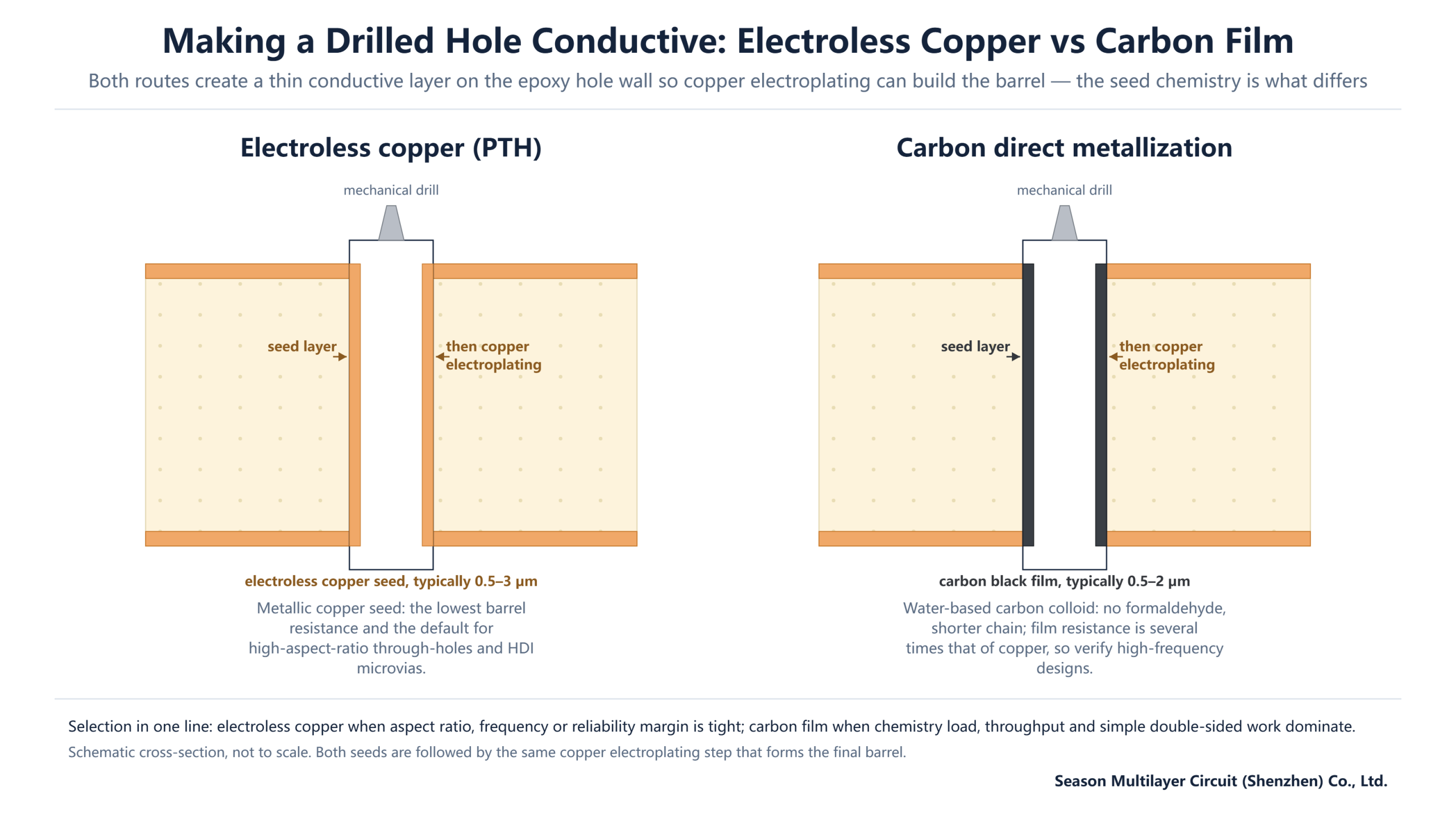
There are two ways to create that seed. The classical route is electroless copper plating, a chemical reduction that grows metallic copper on the wall. The newer route is carbon-based direct metallization, known on the floor as the black hole process, which adsorbs a conductive carbon film instead. Both are followed by the same electroplating step; the difference is what the plating has to bond to.
The awkward part for buyers is that the seed is invisible in the finished board. A cross-section shows you a copper barrel either way, and both routes can produce beautifully plated holes when the line is disciplined. The differences live in the process margin — how much room the chemistry leaves before coverage thins out, how much monitoring the bath chain needs, and what happens on the day the line is pushed. Understanding those differences is what turns hole metallization from a mystery cost line into a decision you can audit.
Electroless Copper Plating: The Classical Seed
Electroless copper plating deposits copper by chemical reduction alone — a reducing agent in the bath converts copper ions into metal on the catalysed hole wall, with no external current. Before that can happen, the panel walks through a chain of preconditioning baths: desmear to clean smeared resin out of the holes, a conditioner, a palladium–tin catalyst, and an accelerator that exposes the catalytic sites. We walk through that chemistry step by step in the electroless copper deposition process.
The reward for that chain is a true metallic copper seed, typically under a few microns thick, with low electrical resistance and excellent adhesion to the wall. Because the chemistry has been production-proven for decades, it tolerates demanding geometries: deep through-holes, fine laser microvias, and the high layer counts that define modern multilayer work. When a design needs predictable plating in a hard-to-reach place, this is the default answer.
The cost of the capability is the process itself. Six or more baths, each with its own analysis and replenishment schedule, mean more control points per panel, longer total chemistry contact time, and a wastewater stream that needs dedicated treatment. None of this makes electroless copper slow — it runs in every serious plant — but it does make it the heavier of the two routes to operate.
Carbon Direct Metallization: The Condensed Chain
The black hole process replaces chemical reduction with physical adsorption. A water-based colloid of carbon black particles is brought into contact with the hole wall, where the particles attach and form a thin, continuous conductive film. After a rinse and a light micro-etch that strips carbon from the panel faces — so plating starts only in the holes — the panel goes straight into copper electroplating. The whole seed sequence collapses to roughly four baths, and the chemistry contains no formaldehyde.
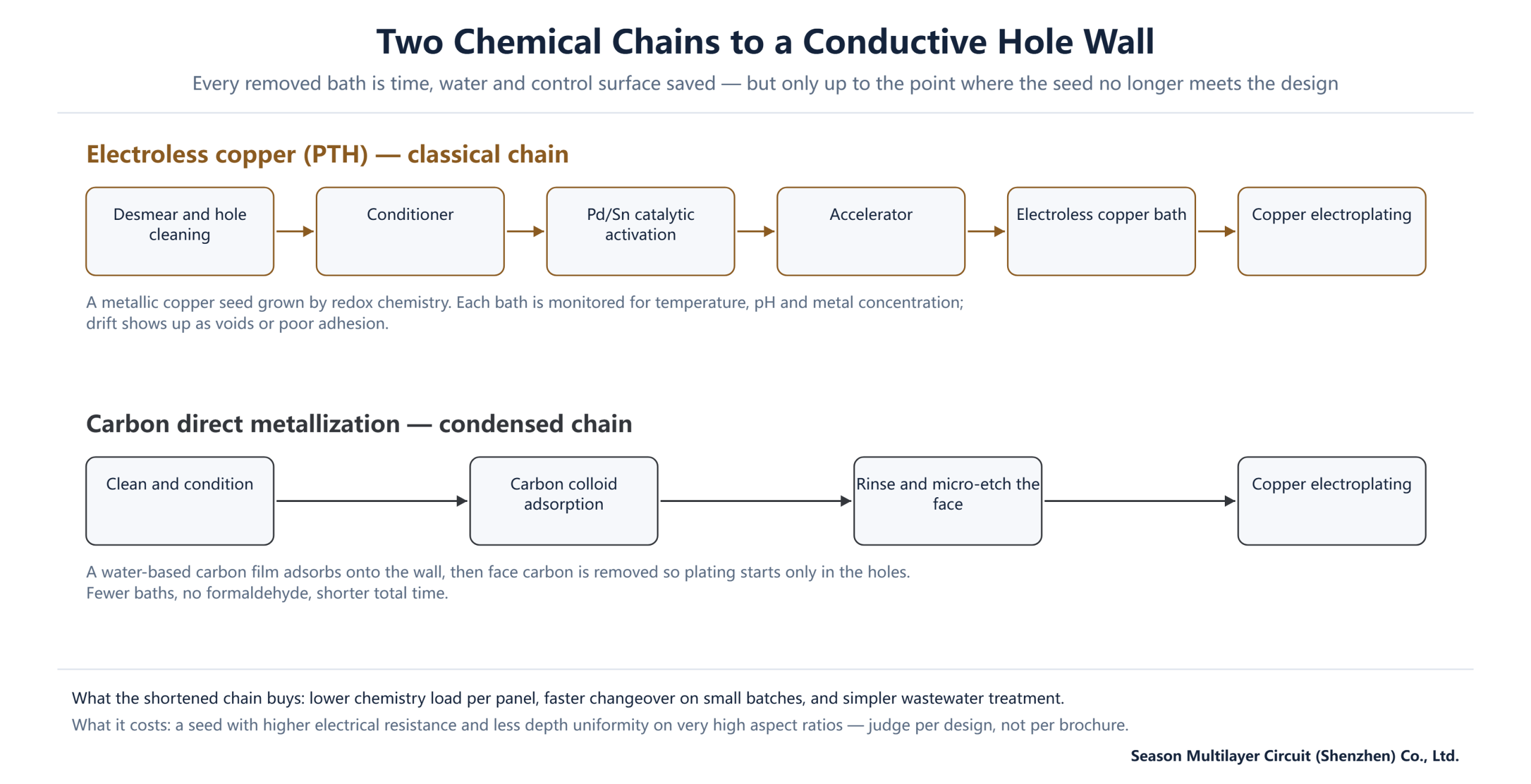
For the plant, the condensed chain means less chemistry per panel, fewer analysis points to hold, faster changeover between small batches, and a simpler effluent stream. For the designer, the important property is electrical: a carbon film conducts, but its resistivity is several times that of copper, and the film is thinner and less forgiving than a metallic seed. Those two facts drive most of the selection logic below.
Black Hole vs Electroless Copper: Side-by-Side Comparison
Put the two routes next to each other and the picture is consistent across the industry. The table below summarises the properties that actually change the decision, expressed the way they are discussed at engineering review.
| Property | Electroless copper (PTH) | Carbon direct metallization |
|---|---|---|
| Seed material | Metallic copper, chemically deposited | Conductive carbon black film |
| Typical seed thickness | Roughly 0.5–3 µm | Roughly 0.5–2 µm |
| Seed resistivity | Metallic copper — low | Several times higher than copper |
| Bath chain | 6+ steps incl. Pd/Sn activation | About 4 steps, no formaldehyde |
| Through-hole aspect ratio comfort | High — the default above 8:1 | Moderate — strongest below 8:1 |
| HDI microvias | Standard practice | Adoption varies by supplier |
| Wastewater and chemistry load | Heavier, dedicated treatment | Lighter, water-based effluent |
| Best suited to | High-reliability and high-layer-count builds | Simple double-sided and mid-range work |
Read the table as a centre of gravity, not as a verdict. A capable plant running a well-maintained carbon line can produce very dependable double-sided and four-layer boards; a careless plant can ruin an electroless copper line just as easily. The rows describe where each process is naturally strongest and where its limits get closer.
Aspect Ratio and HDI: Where the Limits Sit
Aspect ratio — board thickness divided by hole diameter — is the sharpest discriminator between the two seeds. The deeper and narrower the hole, the harder it is to coat the middle of the wall uniformly. As we explain in our aspect ratio and plating limits guide, ratios up to 8:1 are comfortable for any fabricator, 8:1 to 12:1 is normal territory for thick multilayer boards, and beyond 12:1 the job becomes special work.
A metallic copper seed tolerates that depth well because electroless deposition is self-initiating along the whole wall. A carbon film depends on colloid particles reaching the middle of a narrow hole in uniform density, and uniformity is exactly what degrades first in deep, small-diameter holes. That is why direct metallization is most at home on double-sided boards and straightforward four-layer work, and why high-aspect-ratio backplane-style builds stay on electroless copper.
HDI adds a second dimension: laser microvias with small diameters and stacked structures. Electroless copper is the established seed for this work, and the plating know-how that keeps a 10-layer 2-stage HDI stackup consistent is built around it. Carbon-based processes exist in the industry and continue to improve, but adoption on demanding HDI varies from supplier to supplier — which is precisely why it belongs on the engineering-review checklist rather than in the quotation footnote.
There is also a desmear interaction worth knowing. Before either seed is applied, plasma or chemical desmear roughens and cleans the wall so the seed adheres. The conditioning windows differ between a metallic seed that chemically bonds to a catalysed surface and a carbon film that relies on controlled adsorption, so a fabricator switching routes between prototype and production is making a real change — one more reason to keep the same route from first article to volume, or to re-verify when it must change.
Signal Integrity and Reliability Notes
For most digital work the seed layer disappears inside the electroplated barrel, and its higher resistance is irrelevant. The exceptions are designs where barrel quality is doing electrical work: low-level analogue signals, high-frequency transmission structures, and anything where the specification calls out barrel integrity explicitly. In those cases the metallic seed gives the plating a more predictable foundation, and fabricators know it.
Reliability tells a similar story. The failure mechanisms that matter — plating voids, thin spots at the barrel mid-wall, adhesion loss under reflow cycling — are all aggravated by an uneven seed. Our guide to plating voids in microvias shows how a void that starts at the seed becomes a field failure later. This is not an argument that one process always fails and the other never does; it is an argument for matching process margin to how hard the design is.
A practical middle ground exists: some plants run both lines and route boards by difficulty. Simple builds take the fast, light-chemistry route; demanding builds take electroless copper. Asking a supplier which line your board will run on is a legitimate question, and a good one will answer it with panel data rather than marketing.
Verification closes the loop. Cross-section coupons from the panel edges show barrel thickness distribution and any voiding at the seed interface; electrical tests on coupons catch connectivity before assembly. Whichever seed a line uses, the inspection points are the same — what changes between routes is how much statistical margin sits behind them. When you qualify a new fabricator, asking for a cross-section report on a representative hole is the fastest way to see how much margin they actually run.
Cost and Environmental Trade-Offs
The economic comparison is really a comparison of chemistry load. Direct metallization lines carry roughly a third of the bath inventory, use water-based chemistry without formaldehyde, and generate an effluent stream that is markedly easier to treat. Supplier comparisons generally land on total conversion cost in the plating area falling by roughly a third to a half for simple builds — meaningful, though it fades as board complexity rises and the panel ends up on the classical line anyway.
Environmental compliance increasingly factors into sourcing, especially for customers shipping into Europe. A shorter chemical chain means fewer reportable substances to manage and a lighter treatment burden, and RoHS conformity is unaffected either way since the seed layer is buried under plated copper in the finished board. For high-mix plants, the faster changeover of the carbon line also shortens queue time on small prototype batches — sometimes worth as much as the chemistry saving itself.
One more scheduling effect is easy to miss: bath maintenance windows. Electroless copper lines need analysis and replenishment on a fixed rhythm, and a panel released into a tired bath is where adhesion stories begin. Plants that operate both routes can absorb maintenance downtime with less schedule impact because the condensed line keeps running — a resilience benefit that shows up in on-time performance long before it shows up in a cost model.
Choosing Black Hole vs Electroless Copper for Your Build
The decision compresses to a short judgement table. Most designs fall into one of these rows, and the answer follows from the geometry and the application rather than from preference.
| Your build | Route that normally fits | Why |
|---|---|---|
| Simple double-sided or 4-layer consumer board | Carbon direct metallization | Shortest chain, lowest conversion cost, margin to spare |
| 8–12 layer multilayer with through-holes near 8:1 | Either — confirmed at review | Both seeds hold; plant discipline decides |
| Thick backplane-style build above 12:1 | Electroless copper | Deep-hole wall coverage is the whole game |
| HDI with stacked laser microvias | Electroless copper | Established seed for microvia plating reliability |
| High-frequency or low-level analogue design | Electroless copper | Metallic seed gives the most predictable barrel |
| Volume run with tight cost target | Carbon where the design allows | Chemistry and effluent savings compound at volume |
Products show the pattern in practice. A straightforward 8-layer security system board lives comfortably in the region where either seed works and the plant routes by load, while HDI builds default to electroless copper because the microvia plating margin is not worth risking. The same logic scales from prototypes to production.
What to Confirm at Engineering Review
You do not need to specify the seed chemistry yourself — but you should make sure the review covers the points that decide it. This is the checklist we run through with customers on multilayer PCB manufacturing capability before any release to production:
- Finished board thickness and minimum drilled hole diameter, so the aspect ratio is on the table from the first pass.
- Layer count and stackup, including any buried or blind via structures in the build.
- Application class and frequency range, so barrel-dependent requirements are named early.
- Copper weight targets in holes and on surfaces, since plating route and thickness control are linked.
- Acceptance class for the barrel — cross-section criteria, void limits and inspection sampling.
Acceptance criteria for the finished barrel come from the IPC-6012 performance specification; the IPC standards library is the authoritative map if you need to cite a class in your drawing notes.
Capability, not claims, is what these reviews are for. The photographs our plants publish — production halls, AOI stations and the group campus — exist precisely so buyers can see the lines a board will actually run on before release, and the same openness applies to naming the metallization route for your build.

Frequently Asked Questions
What is the black hole process in PCB manufacturing?
It is a direct metallization method that makes the drilled hole wall conductive by adsorbing a thin film of carbon black particles from a water-based colloid. After a micro-etch removes carbon from the panel faces, the board goes into copper electroplating, which builds the final barrel on top of the conductive film.
Is electroless copper plating the same as copper electroplating?
No. Electroless copper deposits metal by chemical reduction with no external current and forms the thin seed on the hole wall. Copper electroplating uses rectifier current to build the barrel to full thickness on top of that seed. Nearly every through-hole board uses both, in that order.
Why does carbon metallization raise concerns on high-frequency designs?
The carbon seed film has a resistivity several times that of metallic copper, so any contribution it makes to the finished barrel is less predictable. For most digital boards it is buried and irrelevant, but for low-level analogue or high-frequency structures designers prefer the metallic seed foundation of electroless copper and the process margin that comes with it.
Which aspect ratio still works with direct metallization?
Direct metallization is strongest at modest aspect ratios — roughly up to 8:1 — which covers double-sided boards and most simple multilayers. Deeper, narrower holes reduce the uniformity of the carbon film at the barrel mid-wall, so high-aspect-ratio builds normally route to electroless copper where deposition self-initiates along the entire wall.
Does the seed choice change hole copper or impedance specifications?
Not directly. Finished hole copper is set by the electroplating step either way, and impedance is fixed by the dielectric geometry and trace copper. The seed influences how reliably those targets are hit — an uneven seed raises void and thin-barrel risk — which is why the choice is treated as a process margin question, not a spec change.
Is direct metallization compliant with RoHS requirements?
Yes. RoHS restricts substances in the finished product, and the seed layer — carbon or copper — is buried under plated copper in the completed board. Direct metallization also avoids formaldehyde-bearing chemistry on the line, which simplifies environmental management even though it does not change the finished-board compliance picture.
How do I know which process my fabricator will use?
Ask. Reputable manufacturers will tell you which metallization line a given build runs on and why, usually during engineering review alongside aspect ratio and stackup confirmation. If a supplier cannot answer, treat it as a signal to look more closely at their process control overall.
Have Your Stackup and Hole Sizes Reviewed Before Release
Send your Gerber data and stackup intent, and the engineering team will confirm the hole metallization route, aspect ratio margin and plating targets before you commit to production. Reviews typically come back with the process route named and any design-side changes flagged — see our PCB manufacturing services to start.