Book Appointment Now

PCB via plugging explained: how resin plugging and solder mask ink plugging differ in process, fill quality, planarity and cost, with a selection table.
PCB Via Plugging: Resin Plugging vs Solder Mask Ink Plugging
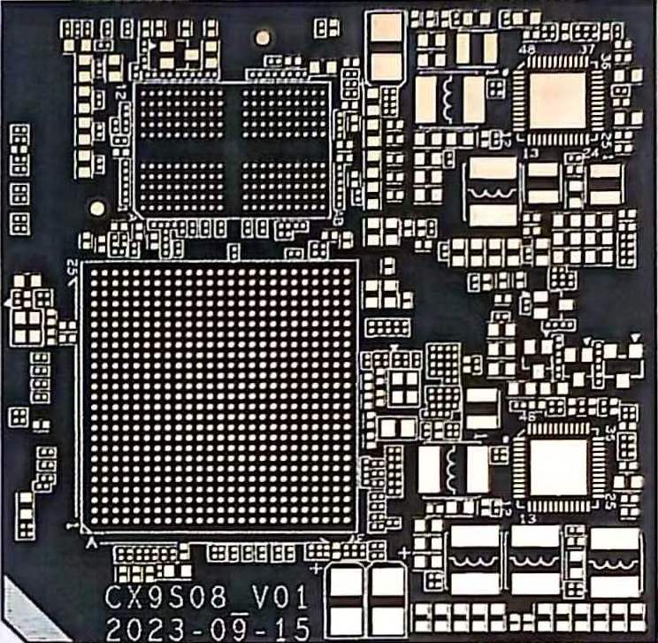
Most boards live or die by their vias long before the first component is soldered. Leave a via open under a BGA pad and solder wicks down the barrel, starving the joint; leave it open anywhere else and it collects flux residue, moisture and stray solder balls during assembly. PCB via plugging closes those holes — but the two mainstream ways of doing it, resin plugging and solder mask ink plugging, behave very differently once the board reaches the line.
This guide walks through both processes step by step, compares them on fill quality, planarity, reliability and cost, and gives a decision table for choosing between them — plus the design rules we check at engineering review before either process is committed to the stack.
Table of Contents
- What PCB Via Plugging Does for Your Board
- The Resin Plugging Process, Step by Step
- Solder Mask Ink Plugging: The Fast, Economical Option
- Resin Plugging vs Solder Mask Ink Plugging at a Glance
- Which PCB Via Plugging Process Should Your Design Use?
- Via Plugging Design Rules: Hole Size, Depth and Aspect Ratio
- Common Via Plugging Defects and How They Are Caught
- Cost and Lead Time: What Drives the Difference
- Where PCB Via Plugging Meets HDI and Via-in-Pad
- FAQ
- Get Your PCB Via Plugging Plan Reviewed With the Stackup
What PCB Via Plugging Does for Your Board
Via plugging fills or closes a drilled hole with a solid material so that its barrel no longer behaves like an open capillary. The problems it prevents fall into four groups. During assembly, an open via next to a pad can wick solder away from the joint or push gas out through the paste. In service, open barrels collect flux residue and moisture, which accelerates oxidation and, on fine-pitch designs, raises the risk of electromigration between neighbouring vias.
The third group is mechanical and electrical: a via placed directly under a component pad — the via-in-pad construction — must be filled and planarised, because an open or dimpled hole creates a void under the solder joint. This is the case where PCB via plugging is not optional. The fourth is simply geometry: on high-density boards, plugging lets vias be placed where an open hole would rob real estate, and it enables stacked via chains in HDI builds.
Not every via needs plugging. Vias in open areas with no solder joint above them are usually tented with solder mask instead, which is cheaper still. The decision is a design decision, and it should be visible in the drill and stack tables rather than left to the fabricator to guess.
The Resin Plugging Process, Step by Step
Resin plugging — often called plate over via fill, or POFV — uses an epoxy resin system to fill the barrel completely, then turns the filled hole back into a solderable pad. The sequence runs in four steps:
- Barrel plating: the hole is drilled and copper-plated as usual, so the via is electrically connected before filling.
- Resin fill: epoxy resin is pressed into the barrel under vacuum or high pressure, eliminating trapped air so the fill is full and bubble-free.
- Cure and planarise: the resin is cured, then the surface is mechanically ground flat so the plug sits flush with the surrounding copper.
- Plate over: a copper layer is plated over the planarised plug, restoring a continuous, solderable metal surface — which is what allows a component pad to sit directly on top.
The planarise-and-plate steps are what separate resin plugging from every cheaper alternative. They add process stages and require dedicated equipment, which is why resin plugging is specified selectively rather than applied to every hole on the board. Where the design needs the plug to carry a pad, though, there is no substitute inside PCB via plugging: only a filled, planarised and plated-over hole gives the assembler a flat, solderable surface.
Solder Mask Ink Plugging: The Fast, Economical Option
Solder mask ink plugging — sometimes called via plugging with mask ink, or hole plugging in the solder mask stage — uses the same liquid photoimageable ink that forms the solder mask, screened or printed into the via openings. The board is then cured, and the plug hardens in place. No planarising step follows, and no copper cap is plated over the plug.
The process has real strengths. It runs on the solder mask line without dedicated fill equipment, so it adds little cost and little lead time; the cured ink is a good insulator and seals the barrel against flux and moisture; and for vias that never see a solder joint, it delivers everything the design actually needs. Mask ink formulations carry flammability and reliability qualifications under UL in the same way laminates do, so the material is not a compromise on safety. For vias that never see a solder joint, it is the workhorse of PCB via plugging.
The limits are equally clear. Because the plug is not planarised, its surface is not flat enough to carry a pad. Fill depth is harder to guarantee on small or deep holes — ink can shrink back during cure and leave a depression or, on narrow barrels, an incomplete fill — and the plug contributes nothing to the mechanical or thermal performance of the joint above it.
Resin Plugging vs Solder Mask Ink Plugging at a Glance
The two processes solve different problems, and the confusion between them causes most of the rework in this area. The table summarises the practical differences:
| Property | Resin plugging (POFV) | Solder mask ink plugging |
|---|---|---|
| Fill material | Epoxy resin system, vacuum or pressure assisted | Liquid photoimageable solder mask ink |
| Fill quality | Full, void-free fill of the barrel | Usually partial-depth; small or deep holes can shrink back on cure |
| Surface after process | Planarised flat, then copper plated over | Cured ink, slightly recessed; no metal cap |
| Solderable pad on top | Yes — the defining capability | No |
| Via-in-pad suitability | Designed for it | Not suitable |
| Corrosion and moisture sealing | Excellent once capped | Good — the ink itself seals the barrel |
| Equipment | Dedicated fill, cure and grinding stages | Runs on the solder mask line |
| Relative cost | Noticeably higher — extra process stages and equipment | Low — marginal addition to the mask stage |
| Typical placement | Pads, stacked microvias, thermal vias under packages | Non-critical vias across the general routing area |
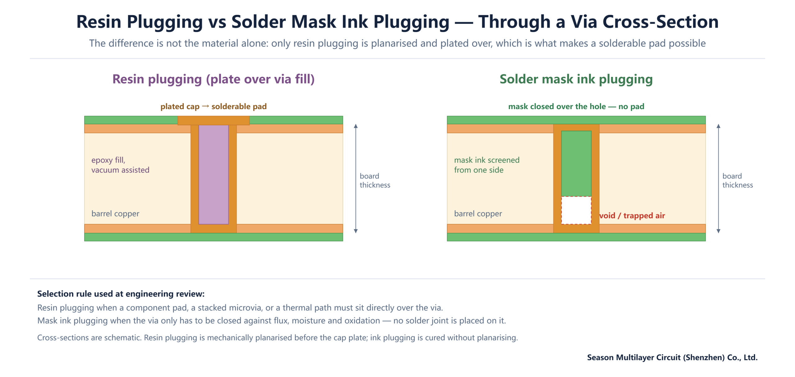
One way to remember the difference: resin plugging rebuilds the surface, while ink plugging closes the opening. If anything needs to be soldered, stacked or thermally coupled on top of the via, only the first one qualifies.
Which PCB Via Plugging Process Should Your Design Use?
Selection between the two PCB via plugging processes is driven by what sits above the via, not by board size or layer count. The table maps common situations to the right process:
| Design situation | Recommended process | Reason |
|---|---|---|
| Via directly under a BGA or QFN pad | Resin plugging | The pad needs a planarised, plated surface; an open or ink-plugged barrel starves or voids the joint |
| Via-in-pad with a stacked microvia above | Resin plugging | Stacked HDI chains require a filled and capped platform — see stacked versus staggered vias |
| Thermal via array under a power package | Resin plugging | Planarisation keeps the package seated; the fill supports the joint across the array |
| Ordinary signal vias between routing layers | Mask ink plugging | No joint above; sealing against flux and moisture is all that is needed |
| Vias in open areas with no component above | Tenting (no plugging) | Cheapest option; solder mask over the annular ring closes the hole adequately |
| Vias that must remain testable | Tenting or leave open | Plugged barrels cannot be probed; agree test points before specifying plugging |
Two caution flags. First, do not specify resin plugging by default across an entire board — it multiplies process steps for holes that did not need them. Second, do not let ink plugging creep under pads to save cost; the failures it produces appear at the assembly line, where they are most expensive to diagnose.
Via Plugging Design Rules: Hole Size, Depth and Aspect Ratio
Plugging quality depends heavily on hole geometry, so a few rules are worth fixing in the design before quotation. Resin plugging is routinely applied to mechanically drilled finished holes in the roughly 0.2 to 0.5 mm range; below that, fill and planarise become progressively harder, and laser microvias in HDI builds are instead filled and capped as part of the microvia process itself. Always confirm the exact hole range with the fabricator at engineering review, because it depends on the equipment generation.
Aspect ratio drives fillability for both processes: the deeper and narrower the barrel, the harder a complete fill becomes, and the more likely shrink-back leaves a depression. The PCB aspect ratio guide covers the plating limits in detail. For plugged vias, keep the drill aspect ratio conservative rather than at the edge of the plating envelope.
Three documentation habits prevent most PCB via plugging rework: mark plugged vias explicitly in the drill file legend rather than burying them in a note; state whether each class of plugged via needs full fill or only sealing; and specify which plugged vias carry pads, so the planarise-and-plate step is priced into the quotation instead of discovered after it.
Common Via Plugging Defects and How They Are Caught
Both processes have characteristic failure modes, and both are detectable before shipment if the inspection plan covers them:
| Defect | Typical cause | Detection and prevention |
|---|---|---|
| Void or hollow fill | Trapped air in the barrel; insufficient vacuum on the fill | Cross-section sampling per lot; vacuum-assisted fill keeps resin void-free |
| Dimple or depression | Resin or ink shrink-back on cure; over-aggressive planarising | Surface flatness checks; depth limits agreed before production |
| Incomplete fill at barrel bottom | Hole too deep or narrow for the process window | Aspect ratio review at quotation; cap hole depth for plugging classes |
| Plug protrusion above surface | Over-fill without adequate planarising | Grind depth control; flatness verification on first article |
| Solder wicking past the plug | Pad placed on an ink-plugged via | Process selection table above — resin plugging with plated cap under pads |
| Ring delamination around plug | Poor adhesion of plug to barrel; contamination | Barrel cleaning before fill; adhesion verified in cross-section |
For via-in-pad constructions, cross-section verification on the first article is the cheapest insurance in the whole process: it confirms full fill, cap integrity and pad flatness in one sample, before volume production inherits the risk.
Cost and Lead Time: What Drives the Difference
The cost gap between the two processes comes from process count, not material price. Mask ink plugging rides on the solder mask stage that nearly every board already goes through, so its addition is marginal. Resin plugging adds a fill cycle, a cure, a mechanical planarising pass and a plating pass — each with its own setup and inspection — so a board with extensive plugged-pad fields costs noticeably more than the same board with ink plugging only, and lead times stretch accordingly.
The variables that move the number most are the count of plugged vias and pads, the smallest hole in the plugged set, and whether pads sit on the plugs. A design that concentrates resin plugging where it is genuinely needed — under the BGA, in the stacked via chain — and uses ink plugging or tenting everywhere else keeps both cost and lead time close to the base process. Quotes should therefore itemise plugging classes rather than quoting the board as one lump.
Lead time for plugging-bearing builds is confirmed at engineering review once the plugged-via map is known; quoting it from the layer count alone consistently underestimates it, because the fill-and-planarise stages, not the copper, set the schedule.
Where PCB Via Plugging Meets HDI and Via-in-Pad
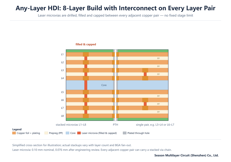
On HDI boards, plugging stops being an option and becomes structure. A stacked microvia chain is built by filling and capping each lower via before the next layer is laminated and drilled — the stacked versus staggered vias comparison shows why the filled, capped platform is what carries the stack. Via-in-pad follows the same logic at component level: the via-in-pad guide covers the design rules, and plating fill is the related route where the barrel is filled with electroplated copper instead of resin, as described in the copper-filled via guide.
The practical division of labour: electroplated fill for holes that must conduct heat or current through the plug, resin plugging for pads and stacked via platforms, mask ink for everything that only needs sealing. Designs that mix all three on one board are common on dense BGA products — a 12-layer HDI core board such as the 12-layer 1-Stage HDI core board carries plugged pads on the BGA field while routing-area vias are handled by mask alone.
If your build uses IPC-4761 via protection types on the drawing, map them to the fabricator’s vocabulary early: the standard’s types for covered, plugged, filled and capped vias translate directly onto the processes above, and a mismatch between drawing callout and process plan is one of the most common sources of requote.
Frequently Asked Questions
What is the difference between resin plugging and solder mask ink plugging?
The two mainstream PCB via plugging processes are not interchangeable. Resin plugging fills the barrel with epoxy, planarises it flat and plates copper over the plug, creating a solderable surface. Solder mask ink plugging presses mask ink into the hole and cures it, sealing the barrel but leaving no flat metal cap. Only resin plugging can carry a component pad on top of the via.
When is resin plugging mandatory instead of mask ink plugging?
Wherever a via sits under a component pad — via-in-pad under BGAs and QFNs — and wherever a stacked microvia needs a filled, capped platform. In both cases the joint or the stack requires a planarised, plated surface that ink plugging cannot provide, and an unplugged barrel would wick solder or trap voids under the pad.
Can solder mask ink plugging carry a pad?
No. The cured ink surface is not planarised and not metal-capped, so it is neither flat nor solderable enough for a reliable joint. Placing a pad on an ink-plugged via typically causes solder starvation or voiding, which is why via-in-pad designs always specify resin plugging with a plated cap instead.
How much does via plugging add to PCB cost?
Mask ink plugging adds little, because it runs on the existing solder mask line. Resin plugging costs noticeably more — it adds fill, cure, planarising and plating stages — and the price scales with the number of plugged pads, the smallest hole size and the number of plugging classes. Concentrating resin plugging where pads demand it keeps the addition contained.
Does via plugging affect thermal performance?
Only marginally by itself. A resin plug is a better thermal path than an air-filled barrel but is not a primary cooling feature; designs that need vias to move heat use electroplated copper fill instead. Resin plugging in thermal via arrays is mainly there to support the package and keep the joint void-free, with conduction as a secondary benefit.
What hole sizes can be resin plugged?
Mechanically drilled finished holes in the roughly 0.2 to 0.5 mm range are the routine window, with smaller and larger holes subject to engineering review because fill quality and planarising both depend on equipment generation. Laser microvias on HDI builds are filled and capped by the microvia process rather than by standard resin plugging.
How should plugged vias be documented in the design files?
Mark plugged vias explicitly in the drill file legend, state whether each class needs full fill or sealing, and flag which plugged vias carry pads so the planarise-and-plate stage is quoted. If your drawing uses IPC-4761 via protection types, confirm the mapping to the fabricator’s process names at quotation to avoid a requote late in the cycle.
Get Your PCB Via Plugging Plan Reviewed With the Stackup
Send your drill files, stack table and pad-via map, and our engineering team will return a plugging plan — which vias get resin, which get mask ink, which stay tented — with the cost and lead-time impact of each class. Start from the PCB manufacturing services page or submit your Gerber set for an engineering review.