Book Appointment Now

A semiconductor package substrate carries the die and connects it to the board. How it works, how it differs from a PCB, and which materials it uses.
Semiconductor Package Substrate Explained: Functions, Materials and Types
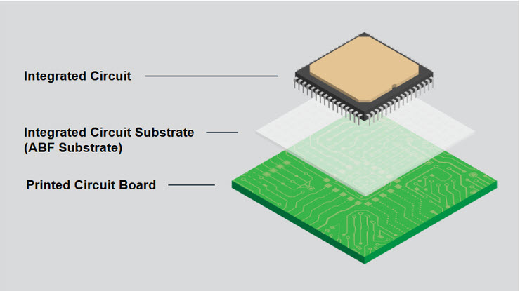
Every hardware engineer eventually meets the moment when a chip refuses to talk to a board directly. Ball pitches shrink, frequencies climb, and the motherboard simply cannot fan out to the die on its own. The gap is bridged by the semiconductor package substrate — the purpose-built circuit board that carries the die, redistributes its connections and shields it from the environment. This guide explains what a package substrate does, how it differs from the PCB it mounts on, and which materials and constructions are used at each performance level.
The distinction matters commercially as well as technically. Substrate-class boards are built to finer geometries and tighter material specifications than conventional multilayer PCBs, which changes how you quote, qualify and source them. By the end of this article you will be able to read a substrate stackup, name the material class a given package needs, and brief a manufacturer with the right vocabulary.
Table of Contents
- What Is a Semiconductor Package Substrate?
- Five Functions a Package Substrate Performs
- Semiconductor Package Substrate vs Conventional PCB
- Package Substrate Materials: From FR-4 Epoxy to BT and ABF
- Package Substrate Types by Structure and Application
- How a Package Substrate Is Manufactured
- Engineering Challenges: Fine Lines, Warpage and Signal Integrity
- Choosing the Right Package Substrate for Your Design
- FAQ
- Get Your Stackup Reviewed Before You Commit
What Is a Semiconductor Package Substrate?
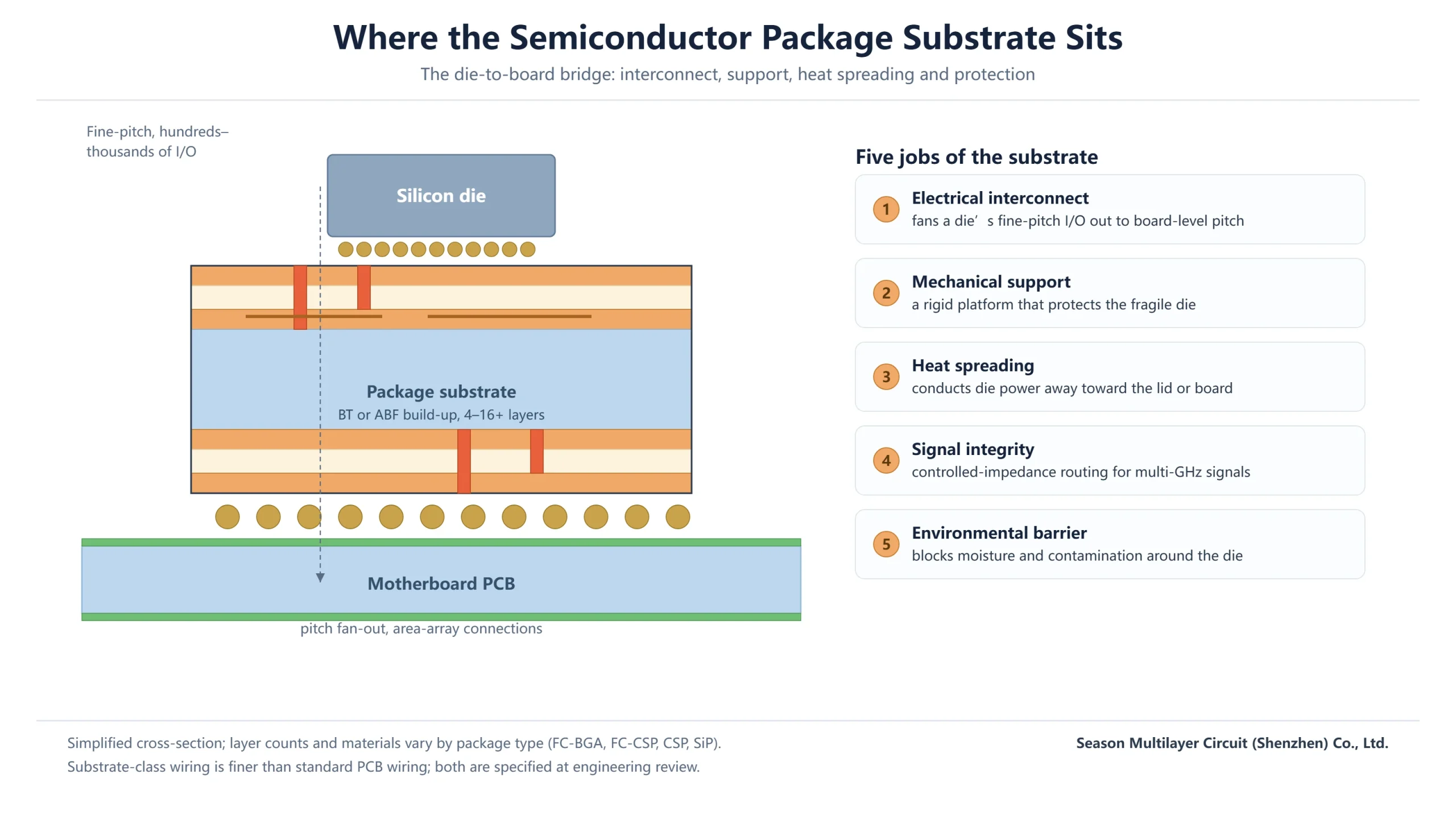
A semiconductor package substrate — also called an IC substrate or package baseboard — is a high-density circuit board designed specifically to mount, connect and protect a semiconductor die. It sits between the chip and the motherboard: on one side, solder bumps or wire bonds meet die-scale pads measured in tens of microns; on the other, an array of solder balls meets board-scale footprints. Without that redistribution layer, a modern processor with thousands of I/O simply cannot be assembled onto a system board.
The substrate is not a passive block of plastic. It is a multilayer wiring structure in its own right, typically four to sixteen or more conductive layers, with its own power and ground planes, controlled-impedance signal routing, and microvias finer than anything on the surrounding board. For many products the substrate is the single most technically demanding laminate in the whole assembly.
Where does it sit relative to ordinary PCB manufacturing? Think of a spectrum. At one end, conventional rigid boards route components at 75 µm line pitch and coarser. At the other end, wafer-level packaging happens inside the fab. The semiconductor package substrate occupies the engineered middle: board-shop processes such as lamination, plating and etching, executed at packaging-class tolerances. For the board-level side of that boundary — laminate classes, glass-transition behaviour and copper foils — see our PCB materials and laminates guide.
Five Functions a Package Substrate Performs
It helps to stop treating the substrate as packaging and start treating it as an active part of the electrical system. It performs five distinct jobs at once, and every one of them shows up in the specification you hand to a supplier.
| Function | What it does | Why it matters |
|---|---|---|
| Electrical interconnect | Fans the die’s fine-pitch I/O out to board-level pitch through microvias and fine lines | Modern dies expose hundreds to thousands of connections within a few square centimetres |
| Mechanical support | Gives the fragile die a rigid platform for handling, assembly and rework | Bare silicon cracks under normal SMT handling loads |
| Heat dissipation | Conducts die power into the lid, the ball array or the board | Power density rises faster than die area on nearly every product generation |
| Signal integrity | Provides controlled-impedance, length-matched routing for multi-GHz signals | Loss and skew budgets are set largely inside the package, before the board even starts |
| Environmental protection | Isolates the die from moisture, dust and chemical attack over years of service | Package-level ingress and corrosion dominate real-world field failures |
None of these functions can be optimised in isolation. A substrate chosen purely for wiring density may lose the heat-spreading path a power device needs; one optimised for thermal conductivity may sacrifice the controlled-impedance environment a serdes channel expects. Good package engineering is the act of balancing all five against the product’s actual duty cycle.
Semiconductor Package Substrate vs Conventional PCB
The two products share manufacturing DNA — imaging, etching, plating, lamination — but they are specified, priced and qualified differently. The table below is the comparison buyers most often need when a sourcing team treats a substrate quote like a multilayer quote and cannot understand the price gap.
| Attribute | Package substrate | Conventional PCB |
|---|---|---|
| Primary role | Chip carrier between die and system board | System platform that mounts all components |
| Line width and space | Down to around 10 µm in advanced FC-BGA builds | Typically 75 µm and above; dense HDI bridges the gap near the 50 µm class |
| Dielectric system | BT resin, ABF build-up films, engineered ceramics | FR-4 family, mid-loss and low-loss laminates |
| Typical layer count | 4 to 16+ build-up layers in a small footprint | 2 to 30 layers across a larger panel |
| Flatness demand | Tens of microns across the whole package | Bow and twist limits measured over a full panel |
| Failure consequence | Assembled die plus substrate both scrapped | Board-level rework or replacement |
The last row deserves emphasis. Because a substrate carries a die that may be worth many times the substrate itself, yield discipline dominates its economics. Every process step is qualified not just for function but for the probability that a defect deeper in the build will scrap an already-expensive component. That is why substrate-class fabrication invests so heavily in inspection and why the wiring specification is written so conservatively.
Package Substrate Materials: From FR-4 Epoxy to BT and ABF
Material choice sets the ceiling for everything else: how fine the wiring can go, how much heat the package survives, how little signal is lost at speed. The industry has moved through four broad material generations, and all four are still in service somewhere.
| Generation | Material class | Strengths | Trade-offs |
|---|---|---|---|
| Conventional organic | FR-4 epoxy glass | Mature, economical, universally available | Coarse wiring capability, thermal expansion mismatch with silicon |
| Ceramic | Oxide and nitride engineered ceramics | Excellent heat conduction, expansion close to silicon, hermetic behaviour | Higher cost and harder processing limit volume use |
| Advanced organic | BT resin and ABF build-up films | Fine-line capability, good high-frequency behaviour, scalable in volume | Requires disciplined sequential lamination and plating control |
| Emerging | Glass cores and new low-loss films | Very flat, dimensionally stable, low electrical loss | Supply base still maturing for volume builds |
Two of those generations deserve their own reading. BT resin — bismaleimide triazine — remains the workhorse where moisture resistance and reflow stability matter most, especially in memory and RF module packages; we cover it in detail in our BT substrate guide. ABF film, an epoxy build-up material originally developed for flip-chip BGA packages, is the default wherever very fine lines and stacked microvias are required, as our ABF substrate guide explains. Glass, the newest entrant, is covered in our glass substrate explainer.
Whatever the resin system, flammability and long-term reliability are qualified against recognised laboratory programs — most buyers start from the UL 94 V-0 flammability classification and add moisture-sensitivity and thermal-cycling requirements on top. Confirm the exact certification status of the laminate lot with your supplier rather than assuming a data-sheet value transfers to your build.
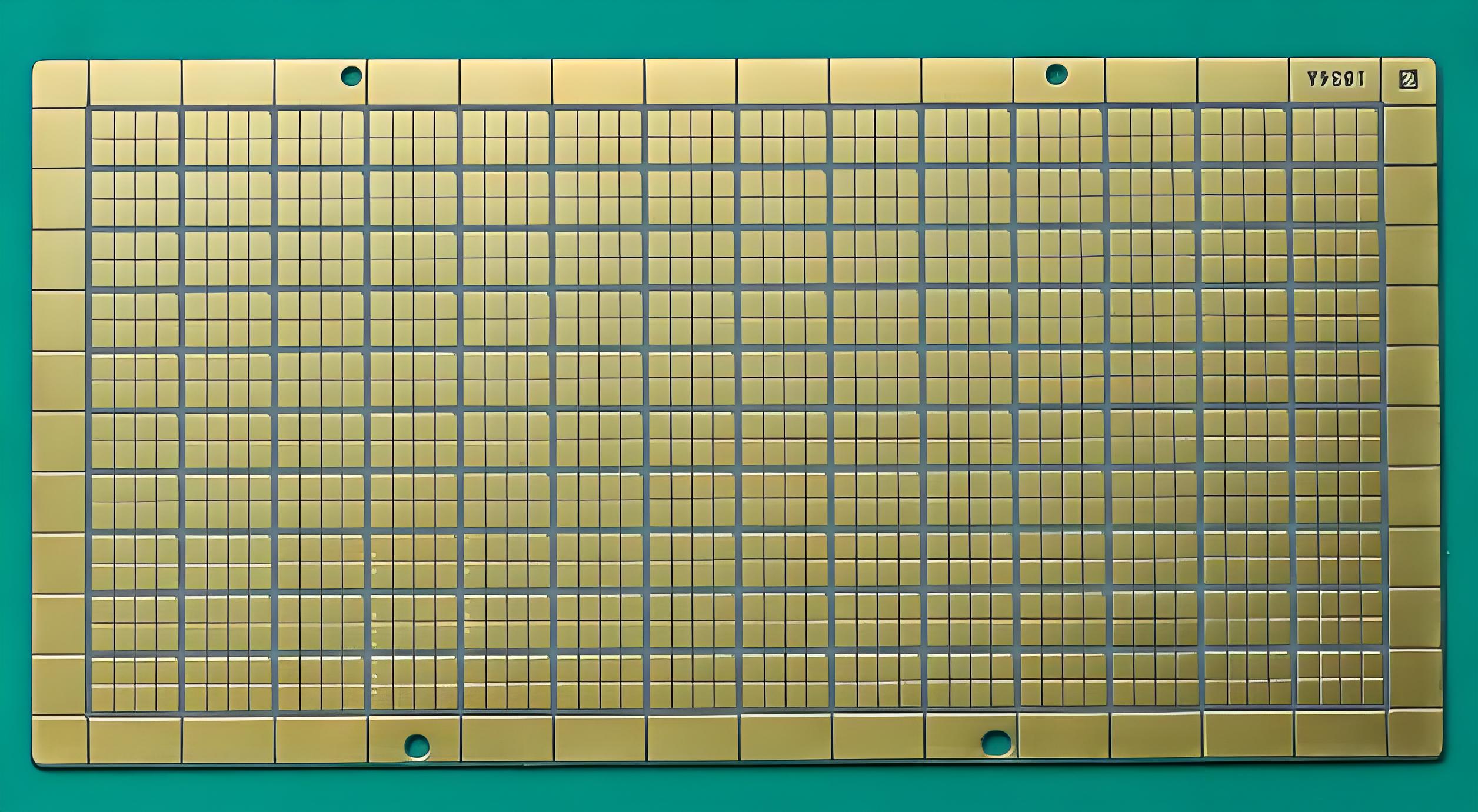
Package Substrate Types by Structure and Application
Classification depends on which axis you care about, and datasheets are rarely consistent about it. Three axes cover nearly every conversation a buyer will have.
| Classification axis | Classes | Where each fits |
|---|---|---|
| By rigidity | Rigid, flexible, and rigid-flex hybrids | Rigid carriers dominate processors and memory; flex and rigid-flex serve wearables and camera modules |
| By construction | Single- and double-sided, multilayer, sequential build-up | Build-up classes serve fine-pitch FC-BGA, CSP and SiP formats |
| By application | Memory, processor, RF module, image-sensor and MEMS carriers | Each application sets its own loss, thermal and reliability budget |
Construction is the axis with the most cost leverage. A package built from a laminated multilayer core with a single build-up stage on each side is a fundamentally different product from one that stacks three or more microvia stages per side, even if the finished footprints are identical. The wiring capability may look similar on paper; the lamination cycles, drilling passes and yield risks are not. When you compare substrate quotations, ask specifically how many build-up stages and lamination cycles each quote assumes, because that single question explains most of the spread between bids.
Application classes add their own vocabulary. Memory packages emphasise moisture robustness and cost at moderate wiring density. Processor and accelerator packages push line width, layer count and power delivery simultaneously. RF modules prioritise low-loss dielectrics and stable impedance over temperature and humidity. Naming your application class early in the RFQ prevents the most common failure, which is a supplier quoting the wrong construction entirely.
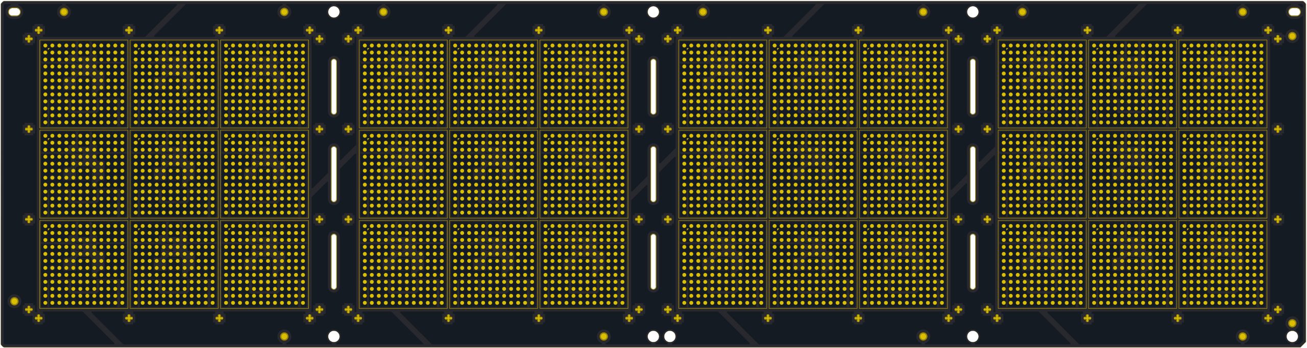
How a Package Substrate Is Manufactured
The process flow reads like conventional PCB fabrication with the tolerances tightened by an order of magnitude. The steps that define quality are these:
- Circuit formation by semi-additive patterning, which plates the finest traces rather than etching them down from full copper
- Sequential build-up lamination: coat or laminate the dielectric, laser-drill the microvia, then desmear and fill it with copper before the next layer
- Via protection with resin plugging or electroplated fill wherever stacked or via-in-pad structures must stay planar
- Solder-mask and surface finishing, typically ENIG where pad corrosion resistance matters or OSP on cost-driven builds
- Singulation with tight edge quality, because brittle substrates chip more readily than FR-4 panels
Two process details dominate yield conversations. First, microvia formation: laser-drilled holes at packaging diameters need clean desmear and void-free copper fill, or the via becomes a latent reliability defect. Second, registration: each build-up layer must align to the layers below within a few microns over the whole panel, which is why substrate fabrication runs at controlled temperatures and invests in precision exposure tooling. Alignment with the IPC standards family — maintained today by the Global Electronics Association — gives buyers and suppliers a shared workmanship language for both areas.
Engineering Challenges: Fine Lines, Warpage and Signal Integrity
Fine-line formation is the challenge most often discussed, because I/O counts keep climbing while die sizes do not. Moving below ten-micron line pitch stresses every step from photoresist chemistry to copper plating uniformity, and each step that drifts shows up as opens or shorts at final test. The practical consequence for buyers is that substrate quotations should be evaluated together with process-capability data, not just dimensional promises.
Warpage is the quieter problem. A package substrate is a thin, asymmetric laminate that cycles through reflow temperatures two or three times before it reaches the customer. Differential expansion between copper, resin and — where present — a stiffener or lid tries to curl the package at every cycle. Excessive warpage shows up downstream as poor ball attachment, solder bridging or corner cracks during board assembly, long after the substrate passed its own inspection. Flatness specifications and simulation data therefore belong in the RFQ alongside electrical parameters.
Signal integrity completes the triad. At package-scale geometries, the substrate is effectively the first transmission-line segment of every high-speed channel, and its via stubs, plane cutouts and dielectric loss set the ceiling the board can never recover. designs that treat the substrate as transparent routinely discover the truth at system bring-up, when the channel budget no longer closes. The remedy is co-planning: the substrate stackup and the board stackup should be engineered in the same conversation.
Choosing the Right Package Substrate for Your Design
Most substrate decisions reduce to six questions, asked in this order:
- How many I/O does the die expose, and at what pitch? This decides whether a leadframe can still do the job or a substrate is unavoidable
- How fine must the wiring be? Line-width demand picks the material class before anything else does
- How much power does the die dissipate, and through which path? Thermal routing is designed, not improvised
- What frequencies must the package carry? Loss and impedance targets follow from the channel budget
- What environment and lifetime does the product face? Moisture, temperature cycling and vibration all price into the construction
- What volumes and phases does the programme need? Prototype-class and volume-class substrates are often built on different flows
Answering those questions produces a stackup sketch and a wiring budget that a supplier can quote meaningfully. Whatever the class, the handoff starts with clean Gerber data and a written stackup, so the fabricator can price the real build instead of guessing at it. Designs that stay on the board-level side of the line — multilayer and HDI carriers such as our 12-layer 1-stage HDI core board — follow conventional PCB economics, and we review those the same way.
Frequently Asked Questions
What is a semiconductor package substrate?
It is a high-density circuit board that mounts a semiconductor die, fans its fine-pitch I/O out to board-level connections, supports it mechanically and conducts heat away. It sits between the chip and the motherboard and is often called an IC substrate. In wiring density, materials and tolerances it is built to a tighter specification than conventional PCBs.
Is a package substrate the same as a PCB?
No. Both are laminated copper structures, but a package substrate carries one die at packaging-class geometry: finer lines, specialised dielectrics such as BT or ABF, tighter flatness and sequential build-up lamination. A conventional PCB hosts the whole system at coarser pitch. The two are specified and qualified differently even when they share fabrication processes.
Which materials are used in package substrates?
The main classes are FR-4 epoxy glass for legacy builds, engineered ceramics for high-power niches, BT resin for moisture-sensitive memory and RF packages, and ABF build-up film for fine-line flip-chip BGA carriers. Glass cores and new low-loss films are emerging classes. Material choice is driven by line width, frequency, power and cost targets together.
How fine are the lines on a package substrate?
Advanced FC-BGA substrates reach line widths and spaces around ten microns and below. Conventional multilayer PCBs typically work at 75 microns and coarser, with dense HDI boards bridging the gap around the 50 micron class. Each step down in line width raises process difficulty and affects yield, which is why the material class is chosen early.
How much does a package substrate cost relative to a standard PCB?
Expect a substantial multiple of an equivalent-area multilayer panel. Cost scales with build-up stages, layer count, line width and, above all, yield discipline, since a scrapped substrate often scraps the die mounted on it. This is why substrate quotations are compared on construction assumptions rather than on board area alone.
Does every IC need a package substrate?
No. Low-pin-count devices are usually mounted on leadframes, which remain cheaper and perfectly adequate for simple parts. A substrate becomes necessary once I/O density, thermal dissipation or signal integrity requirements exceed what a leadframe can deliver — typically processors, memory, RF modules and image sensors.
When should I specify BT resin versus ABF build-up film?
Choose BT resin where moisture resistance, reflow stability and cost dominate — memory packages and many RF modules. Choose ABF where very fine lines and stacked microvias are required, which is the case for most modern flip-chip BGA processors. If the design sits between the two, ask suppliers to quote both constructions and compare the yield assumptions.
Get Your Stackup Reviewed Before You Commit
Whether your product needs a package-class carrier or a high-density board-level PCB, the cheapest point to catch a specification error is before the first purchase order. Send us your Gerber package and stackup intent, and our engineering team will review the wiring density, material class and build-up assumptions against what your channels and thermal budget actually require — then tell you plainly which side of the substrate line the design sits on.
Season Multilayer Circuit manufactures 2 to 30 layer boards, including 1-stage to 3-stage HDI and any-layer constructions, and advises on material selection for package-adjacent designs. Submit your files through our PCB manufacturing services page for an engineering review and quotation.