Book Appointment Now

Ceramic PCB substrate guide: Al2O3, AlN, Si3N4 and SiC compared — thermal conductivity, CTE, metallization routes, and how to choose by application requirement.
Ceramic PCB Substrates: Material Families, Properties and Selection
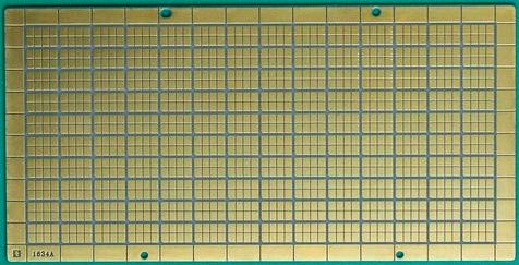
A ceramic PCB substrate replaces the glass-resin laminate of a conventional board with a sintered ceramic — alumina, aluminum nitride, silicon nitride or silicon carbide — and the change rewrites the thermal and electrical rules. Where FR-4 conducts heat at roughly 0.3 W/m·K, even entry-grade alumina manages twenty to thirty times more, and the coefficient of thermal expansion lands close enough to silicon that power dies bond directly to the substrate without a stress-relief layer.
That is why ceramic substrates own the applications organic laminates struggle with: power modules, high-brightness LED packages, automotive sensor carriers and RF front ends. This guide compares the material families with real property numbers, explains the four metallization routes, and finishes with a selection table that maps requirements to materials — plus an honest section on when ceramic is the wrong answer.
Table of Contents
- What Makes a Ceramic PCB Substrate Different
- The Material Families and Where Each Fits
- Thermal and Electrical Properties of a Ceramic PCB Substrate in Context
- Metallization: Thick Film, Thin Film, DBC and AMB
- Decision Table: Choosing the Substrate by Requirement
- Application Areas That Use Ceramic Substrates
- Reliability Behavior: Thermal Cycling, CTE Matching and the Ceramic PCB Substrate
- Where Ceramic Is Not the Right Answer
- Sourcing Questions for a Ceramic Build
- FAQ
- Evaluating a Ceramic Substrate for Your Power or RF Design?
What Makes a Ceramic PCB Substrate Different
Three properties separate a ceramic PCB substrate from any organic laminate, and each one changes what the board can do:
- Thermal conductivity. Heat moves through the substrate itself instead of depending on copper planes and via arrays. A power die on an aluminum nitride substrate sits on a material that conducts heat better than many metals.
- Coefficient of thermal expansion (CTE).
- Hermeticity and stability. Ceramics do not absorb moisture the way epoxy systems do, and they keep their dielectric properties at temperatures where FR-4 has long softened.
The trade-offs are equally real: ceramics are hard, brittle, and processed with completely different equipment than organic laminates. Feature geometry is coarser, layer counts are low, and cost per area runs well above organic builds. The rest of this guide is about when those trade-offs are worth it — and when they are not.
The Material Families and Where Each Fits
Four ceramic families cover nearly all electronics use. The table compares them on the properties that drive selection:
| Material | Thermal conductivity (W/m·K) | CTE (ppm/K) | Character | Typical fit |
|---|---|---|---|---|
| Al2O3, 96% (alumina) | ≈ 24–28 | ≈ 6.5 | Workhorse: strong, cheap, mature supply chain | General power electronics, LED carriers, thick-film circuits |
| Al2O3, 99%+ | ≈ 30 | ≈ 6.6 | Higher purity: better dielectric loss, finer microstructure | RF and microwave substrates, thin-film circuits |
| AlN (aluminum nitride) | ≈ 170–200 | ≈ 4.5 | The thermal champion; CTE close to silicon | High-power modules, laser carriers, thermally critical die-attach |
| Si3N4 (silicon nitride) | ≈ 60–90 (high-grade) | ≈ 3.0–3.5 | The toughness champion: resists crack propagation | Automotive power modules, substrates under mechanical stress |
| SiC (silicon carbide) | ≈ 100–120 | ≈ 4.0 | Extreme temperature and wear tolerance | High-temperature power electronics, harsh-environment modules |
| ZrO2 (zirconia) | ≈ 2–3 | ≈ 10 | Structural ceramic, thermally poor | Mechanical parts, oxygen sensors — rarely a circuit substrate |
Two reading notes. First, zirconia appears on lists of ceramic substrate materials but its conductivity is FR-4 territory — it earns its place through strength, not heat. Second, the silicon nitride numbers depend heavily on grade: standard sintered grades sit near 60 W/m·K while the high-conductivity grades developed for automotive power modules push toward and beyond 90 W/m·K, which is why the substrate datasheet — not the material name — should settle the selection of a ceramic PCB substrate.
Thermal and Electrical Properties of a Ceramic PCB Substrate in Context
Numbers in a table only matter relative to the alternatives. Against an organic laminate system, the ceramic advantage concentrates in three places:
Heat path. On FR-4, device heat must travel through a thermal via array into copper planes — a designed path with losses at every interface. On a ceramic PCB substrate the die-attach pad sits directly on the conductor: heat enters the ceramic immediately. This collapses the thermal resistance budget and frequently eliminates the fan or heatsink a design assumed it needed.
Dimensional stability. Organic laminates move 50+ ppm/K through their thickness across a reflow cycle; ceramics move a fraction of that, and uniformly. Fine-pitch wire-bond and die-attach geometries keep their registration through temperature cycles, which is one reason ceramic carriers dominate hybrid and RF module assembly.
Dielectric behavior at frequency. Alumina’s dielectric constant sits near 9.5–10 with low loss tangent, stable across temperature — well suited to RF microstrip and thin-film filter structures. Aluminum nitride runs slightly lower (~8.8) with even better thermal behavior, making the AlN substrate the default where RF power and heat coexist. For contrast, the high-frequency laminate trade-offs on organic systems are covered in our high-frequency material selection guide, and the standards landscape across both material worlds is indexed by the Global Electronics Association standards library.
Metallization: Thick Film, Thin Film, DBC and AMB
A ceramic substrate becomes a circuit only after metal is applied, and the metallization route determines both the electrical performance and the cost structure:
| Route | Process | Strengths | Watch-outs |
|---|---|---|---|
| Thick film | Screen-printed conductive pastes, fired at high temperature | Lowest cost for simple patterns; rugged; mature supply | Coarser geometry; printing tolerances limit fine pitch |
| Thin film | Sputtered seed + plating or etch, vacuum processed | Fine geometry, excellent edge definition, RF-grade surfaces | Higher cost per area; thickness limits on conductors |
| DBC (direct bonded copper) | Copper foil eutectically bonded to the ceramic at ~1070 °C | Heavy copper on ceramic; excellent heat spreading; strong bond | Needs oxide-forming ceramics (Al2O3, AlN with treatment); copper thickness drives stress |
| AMB (active metal brazing) | Copper brazed with Ag-Cu-Ti active filler | Works on Si3N4 and SiC where DBC cannot; tough joints | Most expensive route;braze-layer control is critical |
Route and material lock together in practice: DBC dominates on alumina and AlN power substrates, while AMB is the enabling technology for silicon nitride — precisely because Si3N4’s toughness pays off most in automotive power modules where thermal cycling is brutal, and those modules need a bonded copper layer DBC cannot provide. When a requirement says ‘ceramic PCB substrate’ for power electronics, the material-and-route pair is really one decision for any ceramic PCB substrate build.
Decision Table: Choosing the Substrate by Requirement
Condensed to the questions buyers actually ask:
| If the dominant requirement is… | Choose | Because | Usual metallization |
|---|---|---|---|
| Balanced cost and performance on power circuits | Al2O3 96% | Mature, strong, adequate conductivity at the lowest ceramic price point | Thick film or DBC |
| Maximum heat extraction from a die | AlN | Highest conductivity in the electronics-ceramic family with silicon-friendly CTE | DBC |
| Thermal cycling survival in automotive power | Si3N4 (high-grade) + AMB | Toughness resists crack growth through thousands of cycles; AMB copper carries the current | AMB |
| RF / microwave performance | Al2O3 99% thin-film grade | Stable dielectric constant and low loss with fine geometry | Thin film |
| Extreme operating temperature or wear environment | SiC | Temperature and wear tolerance beyond the other families | AMB / specialized |
| Mechanical strength first, circuits second | ZrO2 (or rethink) | Strongest ceramic, but conductivity is not better than FR-4 | Thick film (rare) |
One more row worth adding mentally: if the dominant requirement is cost and the power level is modest, the right answer may be an organic laminate with a well-designed copper solution instead of ceramic at all — the subject of the next section.
Application Areas That Use Ceramic Substrates
The application list is concentrated where heat, reliability and size constraints intersect:
- Power electronics modules. IGBT and MOSFET power stages use DBC/AMB ceramic substrates as the electrical-isolation and heat-spreading layer inside the module package.
- Automotive electronics. Engine-bay sensors, ignition drivers and EV powertrain converters value the thermal-cycling survival and temperature stability; silicon nitride substrates were developed largely for this market.
- High-brightness lighting. LED carriers on alumina spread die heat directly, extending lifetime without external cooling.
- RF and microwave. Thin-film alumina circuits feed telecommunications and radar front ends where dielectric stability matters as much as heat.
- Industrial drives and renewable-power converters. Variable-frequency drives, pump controls and solar inverters use ceramic-based power stages for lifetime under continuous load.
The common thread is duty cycle and consequence: applications that run hot continuously, cycle thermally for years, or cannot afford a cooling failure are the ones that pay the ceramic premium voluntarily.
Reliability Behavior: Thermal Cycling, CTE Matching and the Ceramic PCB Substrate
Ceramic substrates fail differently from organic boards, and the failure modes are predictable:
- Braze/solder-layer fatigue. On DBC and AMB substrates, the copper-ceramic joint and the solder joints above it cycle in shear as temperatures swing. This is the dominant wear-out mechanism in power modules and the reason silicon nitride’s toughness translates directly into module lifetime.
- Ceramic cracking from point loads. Ceramics are strong in compression, weaker in tension, and brittle: mounting screws, clamping fixtures and uneven surfaces concentrate stress. chamfered edges and compliant mounting layers are standard countermeasures.
- Die-attach stress mismatch. Alumina’s CTE (~6.5 ppm/K) is farther from silicon than AlN’s (~4.5 ppm/K); for large dies the choice between them is a stress calculation, not just a thermal one.
None of these modes involves moisture absorption or resin degradation — the failure families that dominate organic boards — which is why ceramic assemblies age so predictably in humid, hot environments. The verification techniques for organic-system reliability are covered in our reliability testing guide; ceramic builds run analogous cycle tests with the substrate-and-joint pair as the unit under test.
Where Ceramic Is Not the Right Answer
Honest selection includes the cases where ceramic PCB substrate economics fail:
- High layer counts and dense routing. Ceramics are 1–2 layer substrates in practice; a design needing 8 signal layers with controlled impedance belongs on an organic multilayer, where the stackup logic is covered in our stackup design guide.
- Heat that spreads, not concentrates. If dissipation is distributed across many small devices, an organic board with connected planes handles it at a fraction of the cost — the design playbook is in our thermal management guide.
- Standard BGAs and fine-pitch SMT. Organic builds match these footprints natively; ceramic coarse geometry and special assembly add cost without benefit.
- Prototypes on a schedule. Ceramic tooling and processing run on different lead-time economics; for early design iterations, organic prototypes iterate faster.
The hybrid pattern is common and sensible: power stage on ceramic where the heat is, control logic on an organic multilayer, connected at the module level. Selecting the boundary between the two is exactly the kind of trade a quotation-phase engineering review should settle. Material-level safety and recognition data for substrate systems is published by UL and applies to ceramic assemblies as well as organic ones.
Sourcing Questions for a Ceramic Build
Ceramic procurement runs on different levers than organic PCB procurement. The questions that matter:
- Which substrate grades are actually stocked and processable — alumina 96% is commodity; high-grade Si3N4 is a supply-chain conversation?
- Which metallization routes are in-house versus partner-processed, and who owns the joint quality?
- What are the minimum feature geometries per route (thick film, DBC, AMB, thin film) for the pattern density in the design?
- How are thermal-cycling or die-shear data provided for the material-route pair, not just the raw substrate?
- What assembly constraints apply — die-attach, wire-bond, SMT on ceramic — and who qualifies the interconnect?
Ceramic is a special-process category rather than a catalog product: the right sequence is to submit the application requirements — power level, operating temperature, environment, assembly method — and let the engineering review settle material, route and geometry together. For the organic-side counterpart of that review, the DFM checklist in our DFM analysis guide shows which questions translate directly and which need ceramic-specific answers.
Frequently Asked Questions
What is a ceramic PCB substrate?
A circuit substrate made from a sintered ceramic — typically alumina (Al2O3), aluminum nitride (AlN), silicon nitride (Si3N4) or silicon carbide (SiC) — instead of glass-resin laminate. Metallization is applied by thick film, thin film, direct bonded copper (DBC) or active metal brazing (AMB), producing a board with far higher thermal conductivity, lower CTE and better temperature stability than organic laminates.
Which ceramic substrate conducts heat best?
Aluminum nitride, at roughly 170–200 W/m·K — about seven times alumina and hundreds of times better than FR-4. Its CTE (~4.5 ppm/K) also sits close to silicon, which reduces die-attach stress. High-grade silicon nitride is the alternative when thermal-cycling toughness matters as much as raw conductivity.
Why is silicon nitride used in automotive power modules?
Toughness. Si3N4 resists crack propagation through thousands of thermal cycles better than any other electronics ceramic, and when paired with AMB copper metallization it becomes the substrate of choice for EV powertrain converters and engine-bay power stages where cycling survival determines module lifetime.
What is the difference between DBC and AMB metallization?
DBC (direct bonded copper) eutectically bonds copper foil to oxide-forming ceramics like Al2O3 and treated AlN at around 1070 °C. AMB (active metal brazing) uses a silver-copper-titanium filler to bond copper to ceramics that lack the oxide mechanism, such as Si3N4 and SiC. AMB joints are tougher but costlier; the two routes dominate different material families.
Is alumina always the cheapest ceramic option?
Among the circuit-capable ceramics, yes — 96% alumina has the most mature supply chain and the simplest processing, which is why it is the default for general power electronics and LED carriers. The premium materials (AlN, high-grade Si3N4, SiC) buy conductivity or toughness, not price.
Can ceramic substrates replace multilayer FR-4 boards?
No, not for complex routing. Ceramic substrates are practically 1–2 layer carriers with coarser geometry; a design needing many signal layers, controlled impedance and fine-pitch SMT belongs on an organic multilayer. The common architecture pairs a ceramic power stage with an organic control board at the module level.
How does the dielectric constant of alumina affect RF design?
Alumina’s dielectric constant (~9.5–10) is higher than organic laminates (~3–4), so transmission-line geometries are physically smaller for the same impedance — useful for compact RF circuits. Thin-film processing provides the edge definition those geometries need, and the dielectric properties are stable across temperature, which simplifies filter and matching-network design.
When should a design stay on FR-4 instead of moving to ceramic?
When heat is distributed rather than concentrated, when the design needs multiple layers or fine-pitch SMT, when cost per area dominates, or when fast prototyping matters. An organic board with a well-designed copper solution — planes, thermal vias, appropriate copper weight — resolves most moderate thermal problems at a fraction of ceramic’s cost.
Evaluating a Ceramic Substrate for Your Power or RF Design?
Send the power level, operating temperature, environment and assembly method, and our engineering team will assess whether a ceramic PCB substrate fits — including the material-and-metallization pair, feature geometry and assembly constraints. Ceramic is a special-process category: every requirement is reviewed by engineering before quotation, and feedback typically comes back the same day.
Season PCB direct: Tel (+86) 18681528532 | WhatsApp +86 18681528532
E-mail: roc@season-pcb.com