Book Appointment Now

PCB thermal management by design: thermal via arrays, copper planes, airflow-aware placement, and the laminate choices that move heat instead of trapping it.
PCB Thermal Management: How to Move Heat Out of the Board by Design
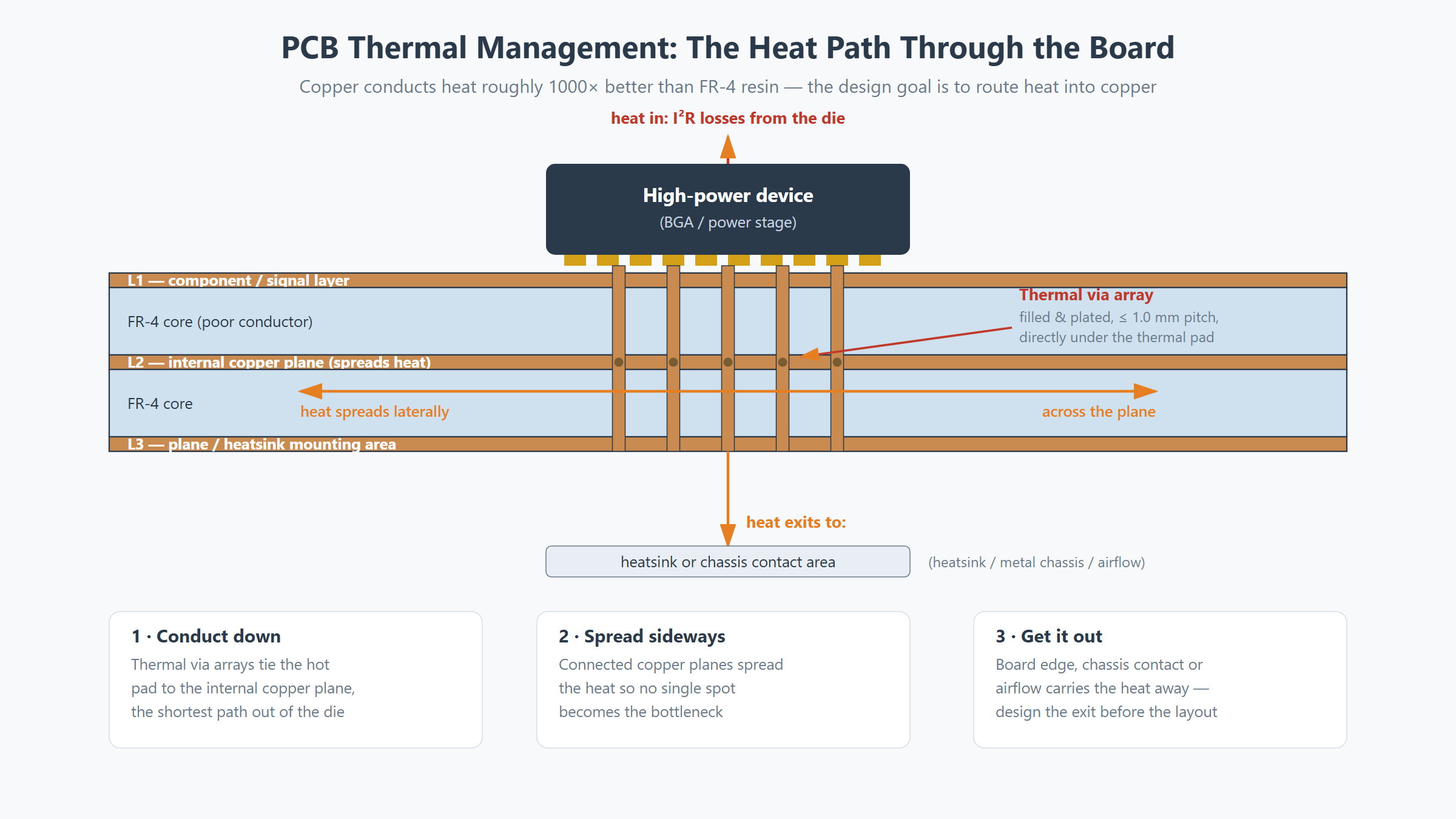
Every watt a board dissipates has to travel somewhere — through solder, copper, resin, and finally into air or a chassis. PCB thermal management is the discipline of planning that journey deliberately instead of letting the die find its own path. The physics is unforgiving: FR-4 resin conducts heat roughly a thousand times worse than copper, so a design that leaves the heat sitting on resin is a design that runs hot no matter what the airflow does.
The good news is that the effective techniques are all ordinary PCB features — thermal vias, connected copper planes, honest copper weights, and placement that respects airflow. This guide organizes them into a decision flow: move heat down from the die, spread it laterally through copper, and get it out of the board — with the tables and design rules for each step.
Table of Contents
- Where the Heat Actually Goes — and Why FR-4 Is the Bottleneck
- Thermal Vias: The Workhorse of PCB Thermal Management
- Copper Weight and Planes: Spreading Heat Laterally
- Placement and Airflow: Layout Rules That Cost Nothing
- Decision Table: Matching the Cooling Strategy to the Power Level
- Laminate Choices That Move Heat
- Verifying PCB Thermal Management: Checks That Catch Trouble Early
- What to Confirm with the Fabricator Before Layout Freezes
- FAQ
- Planning a Thermally Demanding Build?
Where the Heat Actually Goes — and Why FR-4 Is the Bottleneck
Heat generated by a device has exactly three destinations: conduct into the board, radiate into nearby air, or conduct out through the package into a heatsink. For most power levels, conduction into the board dominates — and there the resin system is the obstacle. Typical in-plane thermal conductivity: copper ≈ 390 W/m·K, FR-4 resin ≈ 0.3 W/m·K. Every millimeter a watt travels through bare resin is a millimeter where the temperature gradient steepens.
| Path segment | Thermal conductivity (typical) | Design implication |
|---|---|---|
| Copper trace / plane (in-plane) | ≈ 390 W/m·K | Copper is the heat highway — maximize the copper the heat can reach |
| Copper via barrel (z-axis) | ≈ 390 W/m·K (geometry-limited) | Vias are the elevator between layers — count and pitch matter |
| FR-4 resin (any direction) | ≈ 0.3 W/m·K | Resin is the wall — minimize the resin fraction in the heat path |
| Solder joint (under a pad) | ≈ 50 W/m·K | The joint helps, but only if the pad connects to copper, not to a void |
| Still air | ≈ 0.026 W/m·K | Air is nearly an insulator until it moves — airflow planning is part of the design |
Reading the table bottom-up explains most thermal surprises: a pad that connects to a filled thermal via reaches copper within a millimeter; a pad that floats over resin reaches nothing. The rest of this guide is about making the first case the default. The standards context for acceptance and testing is indexed by the Global Electronics Association standards library.
Thermal Vias: The Workhorse of PCB Thermal Management
A thermal via is a drilled, plated hole placed under or beside a heat-generating pad to give the z-axis a copper path down into the stack. Three parameters control how well an array works:
- Pitch. Arrays at roughly 0.8–1.2 mm pitch under the thermal pad are the common working range; beyond about 1.5 mm pitch the resin gaps between vias start to dominate.
- Fill. Unfilled vias trap air and starve the solder joint during reflow — solder wicks into the barrel and the pad starves. Filled-and-capped vias solve both problems and are standard under BGAs in thermally demanding designs; the process trade-offs are in our via-in-pad guide.
- Depth of connection. A via that connects the pad to one thin inner trace moves little heat; one that lands on a solid internal plane moves a lot. The via is only as good as the copper it lands on.
For via-in-pad designs the array also serves assembly: the filled pad stays flat and the void risk disappears. Where the thermal budget is dominated by a single large device, the array under its exposed pad is usually the highest-leverage change available — it costs layout effort, not board cost.
Copper Weight and Planes: Spreading Heat Laterally
Once heat reaches an internal plane, the plane spreads it laterally — and spreading is what turns a local hot spot into a manageable board-level temperature rise. The spreading ability scales with copper cross-section, which is why heavier copper does double duty as current capacity and thermal capacity.
| Copper weight | Nominal thickness | Relative lateral heat spreading | Typical role in thermal design |
|---|---|---|---|
| 1 oz (35 µm) | 35 µm | Baseline | Signal layers; thin planes on cost-driven builds |
| 2 oz (70 µm) | 70 µm | ≈ 2× baseline | Power layers; internal planes under concentrated loads |
| 3–4 oz | 105–140 µm | ≈ 3–4× baseline | Dedicated thermal spreader layers under high-power devices |
| Heavy copper, 6 oz and above | ≥ 210 µm | Strong spreading; also acts as a busbar | Power conversion, welding-class current, planar magnetics |
The second column is the lever most designs underuse: a dedicated 2 oz internal plane directly under the hot region often outperforms adding airflow. For PCB thermal management under concentrated loads, heavy copper beyond 4 oz is a capability conversation with the fabricator rather than a catalog option — the design rules and process realities are covered in our heavy copper design guide. Plane connectivity matters as much as weight: a plane broken into islands by poor anti-pad planning stops spreading exactly where it is needed most.
Placement and Airflow: Layout Rules That Cost Nothing
Placement decisions shape the thermal result before any via or plane does. The working rules, in the order they pay off:
- Separate heat generators. Clustered power devices stack their thermal footprints; spacing them lets each one use board copper the others are not saturating.
- Respect the airflow direction. Temperature-sensitive and low-power parts belong upstream, where incoming air is coolest; high-power, heat-tolerant parts belong downstream.
- Push big heat sources toward the board edge or the mounting zone where a heatsink, chassis contact or conduction path exists — shortening the exit path beats improving every internal one.
- Keep thermal riders off signal geometry. A thermal via array under a sensitive analog pad changes its environment; plan the arrays where they do not fight impedance-controlled regions.
- Leave copper continuity under hot regions. Hatched pours with sparse connectivity look thermally friendly in layout tools but perform poorly; solid, well-connected copper wins.
These rules interact with the mechanical side of the board: asymmetric copper placement drives warpage, and warped boards handle heat worse and assemble worse. The mechanical coupling is covered in our warpage causes and prevention guide.
Decision Table: Matching the Cooling Strategy to the Power Level
The techniques stack, and the right starting point depends on how much heat the board must move. The table maps rough power levels per major device to the strategy set that usually closes the gap:
| Heat situation (per major device) | First-line strategy | Add when needed | Fabricator conversation |
|---|---|---|---|
| Below ~1 W, spread across the board | 1 oz planes + natural convection placement | Local thermal vias under the hottest IC | None — standard build |
| 1–5 W concentrated on one device | Thermal via array (filled) + 2 oz internal plane under it | Copper enlargement on the pad; airflow path in the enclosure | Via fill capability; plane connectivity |
| 5–20 W, several devices | Dedicated 2–3 oz thermal spreader layers; device placement mapped to airflow | Heatsink mounting provisions; board-edge conduction zones | Copper weight limits; press capability for thicker copper |
| 20 W+ or sealed enclosures | Heavy copper planes (4 oz+); thermal interface to chassis designed in | Separated power stage; simulation-driven via farms | Heavy copper process (see capability), registration at high copper weights |
For PCB thermal management the escalation path matters more than any single row: thermal problems solved at the layout stage cost a design iteration, while the same problems discovered at pilot build cost a respin. That is why the table’s last column — the fabricator conversation — belongs in the quotation phase, not after the first thermal test fails.
Laminate Choices That Move Heat
Resin system choice changes the board’s baseline conductivity modestly but reliably, and — more importantly — it changes how the system survives heat. The selection factors that matter:
- Glass style and resin content. Denser glass wetting reduces the resin channels that trap heat and enables CAF; the mechanics are covered in our prepreg selection guide.
- Tg and decomposition temperature. A system with comfortable margin above the reflow peak keeps its structure — and its copper bond — through multiple thermal cycles; the grade ladder is explained in our laminate selection guide.
- Thermally enhanced laminates. Filled-resin systems with ceramic filler raise in-plane and z-axis conductivity meaningfully; they are the middle option between standard FR-4 and specialty substrates when the power budget sits between the two.
- Metal-backed constructions. For very high single-device power, an insulating metal carrier bonded to the stack moves heat at a scale FR-4 systems cannot. These are a distinct capability with their own design rules — a separate conversation at quotation, not a drop-in swap.
One caution keeps designs out of trouble: material datasheets quote conductivity in specific directions and test conditions, and in-plane versus z-axis values differ by an order of magnitude on some systems. Ask for the direction relevant to your heat path before comparing datasheets.
Verifying PCB Thermal Management: Checks That Catch Trouble Early
Thermal verification before the pilot build does not require a full simulation suite. The escalating checks:
- Copper connectivity audit. Every thermal via array should trace to a solid plane, not a floating island — this is a five-minute review in most CAD tools and catches the most common silent failure.
- Simple spreading estimate. For a single hot device, a spreading-resistance estimate on the plane area gives a defensible first temperature number.
- Thermal simulation when the power density justifies it — most valuable for sealed enclosures and multi-device boards where interactions dominate.
- Pilot-build measurement with thermocouples or an IR camera under realistic airflow, comparing against the estimate rather than a datasheet dream.
- Long-term stability through the reliability suite — thermal cycling exposes the interfaces that heat stresses; the standard flow is described in our reliability testing guide.
The audit-first habit matters because the expensive simulation tools assume the geometry they are given: a thermal via array that is disconnected from its plane simulates fine and performs like the resin it was supposed to bypass.
What to Confirm with the Fabricator Before Layout Freezes
Thermal features touch fabrication capability earlier than most design teams expect. The short question list:
- What is the maximum copper weight per layer on your standard press cycle, and at what layer counts?
- Is via fill (conductive or epoxy) offered on thermal arrays, and what minimum pitch does the fill process support?
- How is plane connectivity handled on builds with multiple internal planes — any registration limits between thermal lands and via arrays?
- For heavy copper or thermally enhanced laminates, what is the current realistic lead time and process window?
- Are thermal coupons (array test vehicles) available for the design, so the array performance can be verified on the actual build?
These five answers determine whether the thermal plan drawn in CAD survives contact with the press floor. For the process context behind them — how copper gets distributed through etch, plating and lamination — the walkthrough is in our PCB manufacturing process guide.
Frequently Asked Questions
What is the most effective single change for PCB thermal management?
For a concentrated heat source, a filled thermal via array connecting the device’s thermal pad to a solid internal copper plane. It shortens the conduction path from millimeters of resin to direct copper contact and costs layout effort rather than board cost.
Do thermal vias need to be filled?
Under BGA and other pad-mounted devices, yes in practice: unfilled vias wick solder during reflow, starving the joint, and trap air that reduces the thermal path. Filled-and-capped vias fix both and are the standard for thermally demanding via-in-pad designs.
How much does heavier copper help with heat?
Lateral heat spreading scales roughly with copper cross-section, so 2 oz spreads about twice as well as 1 oz, and 4 oz about four times. The benefit appears where heat reaches the copper — a heavy plane disconnected from the heat source contributes little.
Where should hot components be placed on the board?
Downstream in the airflow direction, separated from each other so their thermal footprints do not stack, and as close as practical to heatsink, chassis or board-edge conduction zones. Temperature-sensitive parts belong upstream where incoming air is coolest.
Does FR-4 really conduct heat that badly?
Yes — roughly 0.3 W/m·K against copper’s ~390 W/m·K, about a thousand-fold difference. That is why every effective board-level thermal technique is essentially a strategy to route heat into copper and keep it out of resin.
When is a thermally enhanced laminate worth it?
When the power budget sits between what standard FR-4 with good copper design can handle and what a metal-backed construction would cost. Filled-resin systems raise conductivity modestly and also improve glass wetting, which helps long-term reliability. Ask for the conductivity value in the direction of your heat path — in-plane and z-axis differ substantially.
Can thermal problems be found before the pilot build?
The cheapest checks are non-simulation ones: audit that every thermal via array lands on a connected plane, run a spreading estimate for the hottest device, and review placement against the enclosure’s airflow. Simulation earns its cost when power density is high or the enclosure is sealed and interactions dominate.
Why did my board run hot despite thermal vias?
The most common cause is connectivity: the array exists in layout but lands on an isolated copper island or a thin trace instead of a solid plane. The second is pitch — sparse arrays leave resin gaps that dominate the path. Both are layout-stage findings, which is why the connectivity audit comes first in verification.
Planning a Thermally Demanding Build?
Send your power budget, the devices that run hottest, and your target stackup, and our engineering team will confirm the copper weights, via-fill options and plane-connectivity plan that fit — before layout freezes. Production runs from 2 to 30 layers (up to 64 layers for prototypes, subject to per-order review), including heavy copper builds, with process feedback typically the same day.
Season PCB direct: Tel (+86) 18681528532 | WhatsApp +86 18681528532
E-mail: roc@season-pcb.com