Book Appointment Now

A buyer's guide to PCB quality inspection: the visual criteria, coupon tests, electrical test data and AQL sampling plan a shipment must stand behind.
PCB Quality Inspection: The Report Package Every Buyer Should Receive
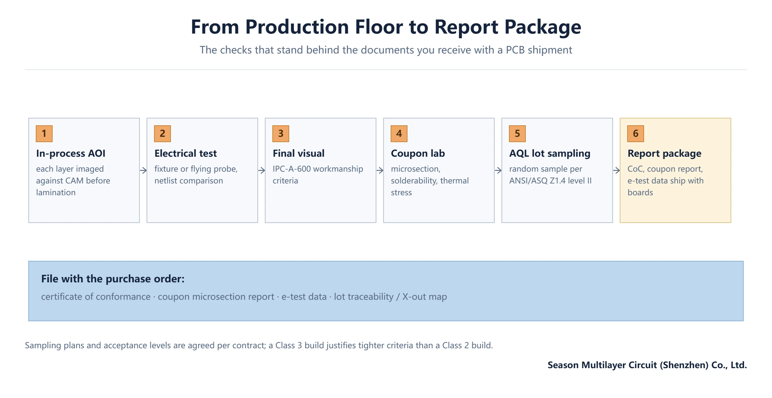
By the time a carton of finished boards reaches your receiving dock, every meaningful decision about their quality has already been made – or skipped – on the fabrication floor. That is why a structured PCB quality inspection routine matters more at the document level than at the microscope level: the fastest way to judge a lot is to check whether the fabricator’s process actually generated the evidence a good process generates, and whether that evidence holds up under sampling.
This guide walks through what a competent inspection package contains, how visual acceptance criteria work under IPC-A-600 Class 2 and Class 3 requirements, what the test coupon proves, how AQL sampling is applied to a shipment, and the specific red flags that justify holding a lot. It is written from the buyer’s side of the transaction, but it is equally useful as a checklist for auditing your own supplier.
Table of Contents
- What PCB Quality Inspection Covers at Receiving
- Visual Acceptance Criteria per IPC-A-600
- The Test Coupon: Your Lot’s Fingerprint
- Electrical Test: Fixtures, Flying Probe and Voting
- How AQL Sampling Works in a PCB Shipment
- An Incoming Inspection Checklist You Can Run Today
- The Report Package: What Each Document Proves
- Red Flags That Justify Holding a Shipment
- How Your Fabricator Should Run PCB Quality Inspection
- FAQ
- Expect the Evidence With Every Shipment
What PCB Quality Inspection Covers at Receiving
Bare-board verification has two layers. The first is lot-level acceptance: a random sample of boards from the shipment is checked against the drawing, the stackup and the applicable workmanship standard, so the decision generalizes to the whole quantity rather than to the handful of boards you happened to open. The second is document verification: the certificate of conformance, coupon reports and electrical test data shipped with the boards, which tell you whether the fabricator tested what they were supposed to test – and whether the results trace back to your lot specifically.
Neither layer substitutes for the other. A spotless report package cannot rescue a lot that fails sampling, and passing boards without traceable reports leave you unable to defend the shipment to your own customer or auditor. Mature incoming PCB quality inspection runs both in parallel, and the paperwork side usually takes less than an hour per lot once the checklist below is in place. If your review keeps surfacing gaps in the documents themselves, our guide on laminate quality and incoming material checks goes one level deeper into the raw-material side.
Visual Acceptance Criteria per IPC-A-600
Visual workmanship is judged against IPC-A-600, the illustrated acceptance standard for printed boards, at the class level named on your drawing – Class 2 for most industrial and commercial products, Class 3 where service demands are higher. The standard defines what counts as an acceptable annular ring, how much solder-mask registration error is tolerable, when a scratch on a conductor becomes a reject, and dozens of similar judgements that would otherwise be argued case by case. The full family of inspection and qualification standards it belongs to is maintained by the Global Electronics Association (IPC standards library).
The practical discipline at receiving is to check the same attributes every time, at the same magnification, on a defined sample. Panel flatness and warpage, edge quality and burrs, solder-mask coverage and alignment, legend legibility, and surface-finish appearance are the five families that catch most visual rejects. Anything cosmetic-but-marginal should be photographed against a ruler and quoted against the standard’s own illustrated limit, not against anyone’s memory of what a previous lot looked like. This keeps the conversation with the fabricator factual and fast.
The Test Coupon: Your Lot’s Fingerprint
A test coupon is a small panel pattern processed alongside your boards, so it experiences exactly the same lamination cycles, drilling and plating chemistry. Its job is to let destructive tests run on representative hardware without sacrificing shippable boards. A proper coupon carries impedance coupon structures for TDR measurement, microsection sites for plating thickness and layer alignment, and bonding sites for solderability and thermal-stress samples.
When the coupon report comes back, read it against your drawing, not against generic capability claims: plating thicknesses against the class minimum, impedance results against the per-layer-pair targets and tolerance band you assigned, and microsection findings against the relevant IPC-6012 criteria. Coupon results that trace to your panel ID are evidence; capability statements that trace to nothing are marketing. Our guide to PCB reliability testing explains how coupon-based tests scale up into a full qualification programme when a new stackup or material enters production.
Electrical Test: Fixtures, Flying Probe and Voting
Every bare board should be electrically tested against the netlist extracted from your Gerber data, so that opens, shorts and isolation failures are caught before the boards ship. High-volume lots run on a fixture built from the netlist, which tests every board in seconds; prototypes and low-volume lots often run on flying-probe machines, which test more slowly but need no fixture and catch the same defect families. Either way, the fabricator’s e-test data should state the method, the netlist source and the result for the lot.
Two details deserve a habit-level check. First, ask whether the test is a netlist comparison against your extracted data or against the fabricator’s own tooling copy – a comparison against the customer netlist is the stronger check and the standard practice. Second, confirm how boards that fail are handled: a documented test-and-repair or test-and-scrap flow, with rejects marked and excluded, is normal; an e-test report that shows zero failures on a dense multilayer lot deserves a closer look at the test setup. For how the board’s electrical structure is actually built up layer by layer, see our overview of the PCB manufacturing process.
How AQL Sampling Works in a PCB Shipment
Checking every board visually at receiving is impractical and adds little, because the fabricator has already screened 100% of the lot in-process. Statistical sampling solves the economics: a random sample, sized by the lot quantity under a scheme such as ANSI/ASQ Z1.4 (ISO 2859-1) at general inspection level II, is inspected in full, and the lot is accepted or rejected depending on how many defect boards appear in the sample. The acceptance quality limit – the AQL – is agreed with the supplier in advance and written into the purchase terms.
The choice of AQL should follow the product’s class and consequences of failure. Lots destined for Class 3 work commonly carry tighter visual acceptance than commercial Class 2 lots, and a fabricator serving both markets should be able to run each lot to its own agreed level. What matters for the buyer is consistency: the same plan applied to every lot, with the sample drawn randomly rather than taken from the top of the carton. If sampling results degrade across consecutive lots, that trend is more informative than any single acceptance.
An Incoming Inspection Checklist You Can Run Today
The table below condenses a working incoming inspection into the checks that earn their time. Run it identically on every lot, record the result per attribute, and the history becomes your strongest negotiating tool with suppliers.
| Check | Method / tool | Accept looks like | Reject trigger |
|---|---|---|---|
| Documentation complete | Compare against PO and drawing | CoC, coupon report, e-test data, lot ID all present and traceable | Missing reports, or results that do not reference your lot |
| Visual workmanship | IPC-A-600 attributes at defined magnification | No reject-class defects in the sample | Any Class-reject defect in the sample |
| Board thickness | Micrometer at coupon or defined points | Within drawing tolerance | Over tolerance on sampled boards |
| Warpage / flatness | Surface plate or straightedge | Within IPC-6012 field allowance for the board shape | Warp beyond allowance |
| Impedance verification | TDR on coupon structures | Per-pair values inside the assigned ±10% / ±8% / ±5% band | Any pair outside its band |
| Microsection | Coupon cross-section vs IPC-6012 | Plating thickness, alignment and plating quality in class | Sub-class plating, ICDs or alignment faults |
| Electrical test status | Review fabricator e-test data | 100% tested, netlist-based, rejects documented | Untested boards or undocumented rejects |
Solderability deserves its own line for boards that will see wave or reflow assembly within a long storage window; our guide to ENIG solderability and black-pad failures covers what a solderability check can and cannot predict. Surface-finish choice is a decision you make before ordering, not at receiving, so lock it in the drawing and hold suppliers to it there.
The Report Package: What Each Document Proves
Documents are where a fabricator’s process discipline becomes visible to outsiders. The four items below are the working core of a bare-board report package, and each one exists to answer a specific question about the lot.
| Document | What it proves | Red flag to watch |
|---|---|---|
| Certificate of conformance | The fabricator formally accepts the lot against your drawing and stated class | Boilerplate CoC that names no drawing revision or class level |
| Coupon test report | Plating thickness, microsection and impedance measured on hardware from your lot | Values with no panel or lot reference, or results copied across lots |
| Electrical test data | Every net checked against a defined netlist source | Method and netlist source not stated; zero failures on dense builds |
| Traceability map | Which serial or X-out marks belong to which panel and lot | No way to relate returned boards to the tested sample |
Keep the package filed with the purchase order. Its value compounds: across lots it becomes a supplier performance record you can quote in reviews, and if a field failure ever needs investigation, this file is what connects the failed board back to the process evidence from the day it was built. Fabricators who run a mature process capability programme produce this paperwork as a by-product of normal operation rather than as a special favour.
Red Flags That Justify Holding a Shipment
Some findings should stop a lot from moving to assembly until they are resolved, whatever the schedule pressure. The list below is deliberately short – these are the patterns with a track record of turning into field failures:
- Coupon results that reference a different lot, panel or date than the boards in the carton.
- Impedance data quoted as a process capability number instead of measured per-pair values from your coupon.
- An e-test report with no stated netlist source, or dense boards reported as tested with an unusually sparse test report.
- Microsection photos reused between shipments, identifiable by identical backing text or timestamps.
- A CoC that does not name the drawing revision shipped against, after an engineering change.
- Visual rejects in the sample concentrated in one area of the panel, suggesting a systematic process fault rather than random variation.
Each of these is cheap to check and hard to fake, which is exactly what makes them useful. A fabricator who trips one of them occasionally deserves a query; one who trips the same flag repeatedly needs a corrective-action conversation, not another purchase order.
How Your Fabricator Should Run PCB Quality Inspection
Everything you check at receiving exists because the fabricator should have checked it earlier, at higher magnification and on more hardware. A capable supplier runs AOI against the CAM data on every layer before lamination, tests 100% of boards electrically, inspects finished boards to the agreed workmanship class, and processes coupons in a lab that can trace every measurement to the panel it came from. Quality management certification such as ISO 9001:2015 frames that discipline – the UL Solutions certification registry, for example, lets you verify a supplier’s certificate directly – and the visible difference is whether test evidence follows each lot out the door.

Incoming PCB quality inspection is deliberately different from reliability qualification. Receiving checks accept or reject the lot in front of you; qualification answers whether the design, stackup and process will survive the product’s lifetime – thermal cycling, mechanical stress and long-term environmental exposure. Buyers who conflate the two either over-test every shipment or skip qualification entirely. Run both, at the right altitude: sampling and document checks per lot, qualification when a new build enters production, and material-level checks on laminates as described in our laminate quality guide.
For automotive-adjacent programmes, supply-chain audits add a factory dimension – process controls, traceability depth and how nonconforming material is quarantined. A 6-layer automotive PCB prototype line that can walk an auditor from raw laminate lot to shipped serial number, with evidence at each step, is showing you the same discipline this guide asks you to verify on paper.
Frequently Asked Questions
What should a PCB inspection report package contain?
At minimum: a certificate of conformance tied to your drawing revision and class, coupon test results (microsection, plating thickness, impedance) traceable to your lot, electrical test data stating the method and netlist source, and a traceability map linking serial or X-out marks to the tested sample. Anything less leaves you unable to defend the shipment downstream.
What does AQL mean in PCB shipments?
AQL is the acceptance quality limit agreed with the supplier for statistical sampling. A random sample, sized by lot quantity under a scheme such as ANSI/ASQ Z1.4 level II, is inspected fully; the lot is accepted or rejected by how many defect boards appear. Tighter AQL values are normal for higher-class products with more severe failure consequences.
Which visual defects justify rejecting a board?
Reject-class defects under IPC-A-600 at your stated class: conductors below minimum width from scratches or nicks, insufficient annular ring, solder-mask exposure on features that must remain covered, delamination or blistering, damaged pads, and warpage beyond the IPC-6012 allowance. Photograph marginal findings against the standard’s illustrated limits rather than arguing from memory.
Do I need a test coupon on every order?
Every multilayer order benefits from one, because the coupon is the only hardware from your lot that can be microsectioned, TDR-measured and solderability-tested without destroying shippable boards. For repeat builds, a coupon per lot keeps capability results traceable; for prototypes it is the difference between evidence and assurances.
How is a bare PCB electrical test performed?
Each board is checked against the netlist extracted from the design data for opens, shorts and isolation. Volume production uses a fixture built from the netlist to test every board quickly; prototypes and low-volume lots often use flying-probe machines. The report should state the method, the netlist source and how rejected boards were handled.
Is incoming inspection the same as reliability testing?
No. Incoming inspection accepts or rejects the lot in front of you using sampling, visual criteria and document checks. Reliability testing qualifies whether the design and process survive lifetime stresses – thermal cycling, mechanical and environmental exposure – and is run when a new build or material enters production. Both matter, but they answer different questions.
Can I rely on the supplier’s certificate of conformance alone?
A CoC is a formal commitment, not evidence. It becomes meaningful when the referenced coupon report, e-test data and traceability map actually exist and match the lot. Treat a CoC that arrives without its supporting documents – or with results that cannot be traced to your panels – as a hold condition, not an acceptance.
Expect the Evidence With Every Shipment
We build the report package into every lot as standard: coupon microsections, per-pair impedance results and full traceability ship with the boards, so your incoming PCB quality inspection starts from evidence rather than promises. Submit your Gerber files and ask for the inspection plan to be quoted with the stackup review.