Book Appointment Now

The PCB lamination process explained: press book construction, prepreg flow, temperature and pressure windows, registration control and the defects it causes.
PCB Lamination Process: How Multilayer Boards Are Pressed and Bonded
Lamination is the step where a multilayer PCB stops being a stack of separate parts and becomes a single board. Every layer-to-layer connection, every impedance reference plane and every thickness tolerance on your drawing depends on how well the PCB lamination process is run — and yet most fabrication drawings say almost nothing about it. When a batch fails with delamination, measling, warpage or layer shift, the root cause is very often traceable to this step.
This guide walks through the process from a buyer’s point of view: what actually goes into the press, how the PCB lamination cycle bonds cores and prepreg into one body, which parameters decide the outcome, how registration and finished thickness are held through the press, and which defects trace back to it. It closes with the questions worth asking a fabricator before your next multilayer build goes to press. For a broader view of how this step fits into the whole chain, see our multilayer PCB manufacturing capability overview.
Table of Contents
- What PCB Lamination Actually Does
- Inside the Press: The Book, Kraft Paper and Steel Plates
- The PCB Lamination Cycle Step by Step
- Prepreg Flow: The Variable Buyers Never See
- Temperature, Pressure and Vacuum Windows
- Registration Through the Press: Controlling Layer Shift
- Finished Thickness, Copper Balance and Warpage
- Laminating Mixed Dielectrics: FR-4 With RF Layers
- PCB Lamination Defects: Causes and Prevention
- FAQ
- Have Your Stackup Reviewed Before It Goes to Press
What PCB Lamination Actually Does
In simple terms, PCB lamination bonds etched inner layers and prepreg sheets under heat and pressure until the resin cures and the whole stack behaves as one solid body. The prepreg — a sheet of glass fabric pre-impregnated with partially cured epoxy — softens as it heats, flows into the copper pattern gaps, and then crosslinks permanently. The chemistry is irreversible: once cured, the board cannot be re-melted or re-laminated.
That is why the step carries so much weight in a quote review. Copper features, plated holes and surface finishes can all be inspected and, within limits, reworked. A lamination defect is different — it is baked into the body of the board. A void between two layers or a layer-to-layer shift is only ever found after the fact, usually at cross-section or at final electrical test, when the panel is already at its highest accumulated value.
- It fixes the dielectric thickness between layers — which directly sets impedance.
- It fixes layer-to-layer registration — which decides whether drilled holes land on their pads.
- It fixes finished board thickness and flatness — which decides SMT and enclosure fit.
- It locks in the material system — once cured, no downstream step can change the resin.
Inside the Press: The Book, Kraft Paper and Steel Plates
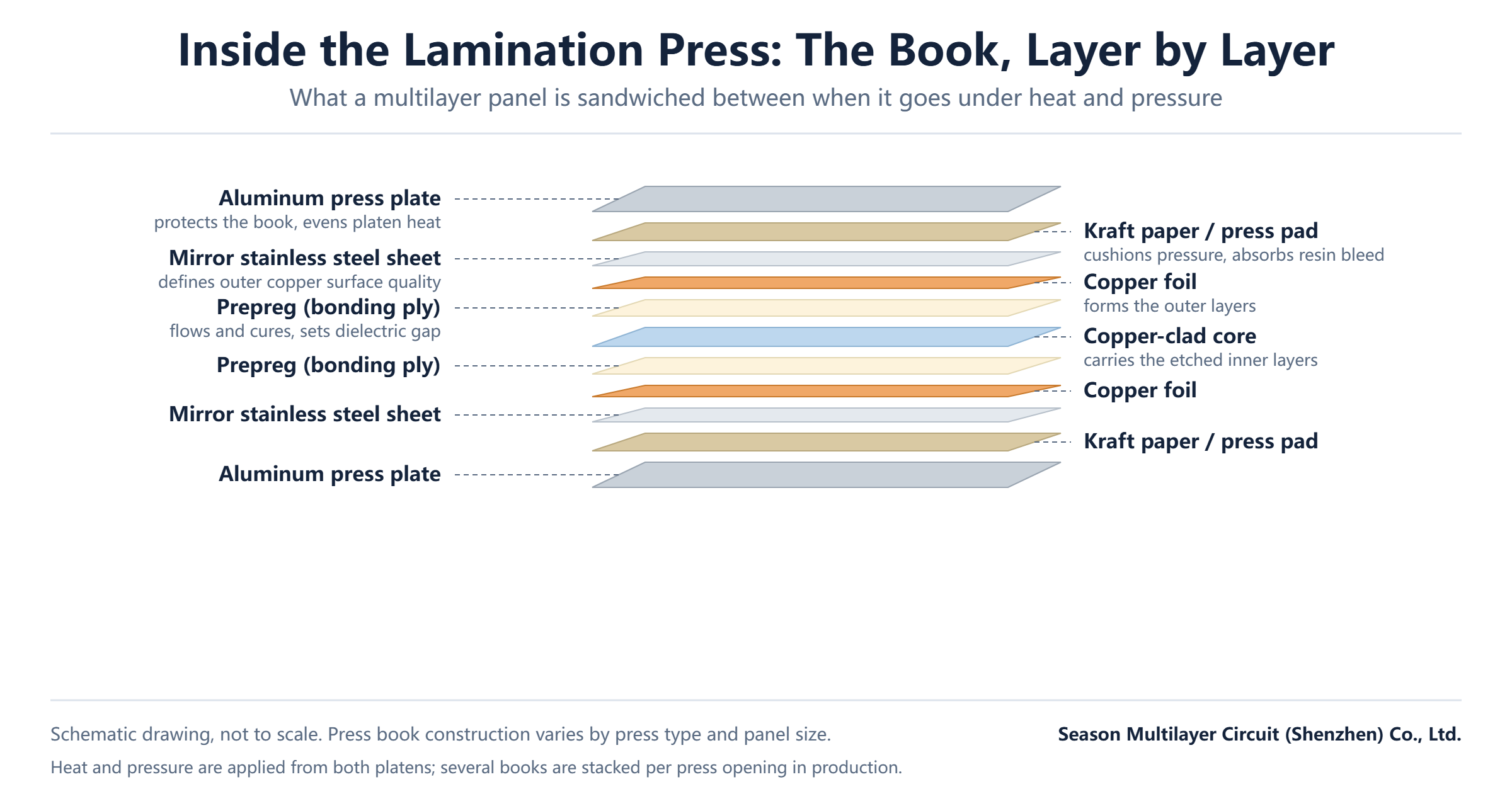
In the PCB lamination process, the action happens inside a “book” — the assembly an operator builds between the press platens. A typical book, from the outside in, is: aluminum press plates, kraft paper or a press pad, a mirror-finish stainless steel sheet, then the copper foil / prepreg / core sandwich itself, and the same sequence mirrored on the other side. Several books are stacked per opening in high-volume presses.
Each of these parts does a specific job. The steel sheets carry the panel surface finish quality — their smoothness is what gives the copper foil side its cosmetic grade. The kraft paper and press pads spread pressure evenly and absorb resin that bleeds out at the edges. The aluminum plates protect the whole book and keep heat transfer uniform. If any layer of the book is contaminated, scratched or worn, that flaw imprints itself onto the panel in the PCB lamination process — which is why press room cleanliness and tooling maintenance matter more than most buyers realize.
| Component | Role in the press book | What happens if it is wrong |
|---|---|---|
| Aluminum press plate | Protects the book, evens out platen heat | Local hot spots, uneven cure across the panel |
| Kraft paper / press pad | Cushions pressure, absorbs resin bleed | Thickness variation, trapped voids at the panel edge |
| Mirror stainless steel sheet | Defines the outer copper surface quality | Scratches or shine marks imprinted on outer layers |
| Release film | Prevents resin sticking to steel | Panel tear-up at de-molding |
| Copper foil | Forms the outer layers | Foil wrinkle, exposed laminate after etch |
| Prepreg (bonding ply) | Bonds layers, sets dielectric gap | Resin starvation or voiding between layers |
| Copper-clad core | Carries the etched inner layers | Inner-layer defects, registration error |
The PCB Lamination Cycle Step by Step
The PCB lamination cycle is a scripted sequence of vacuum, temperature and pressure changes, and every stage has a distinct purpose. The schedule is written per material system, from the resin supplier’s gel-time and DSC data, and the press holds it automatically. Skipping or compressing a stage is the fastest way to bake a defect into the batch.
| Stage | What happens | Why it matters |
|---|---|---|
| Loading and vacuum hold | Book enters the press; vacuum pulls air out before heat rises | Removes trapped air and moisture that would become voids |
| Pre-press | Low pressure while resin warms toward the gel point | Positions the stack without squeezing resin out early |
| Ramp | Temperature climbs on a controlled slope | Controls resin viscosity so it flows before it cures |
| Cure dwell | Full pressure; resin flows, fills and crosslinks | Sets interlayer bond strength and dielectric thickness |
| Cool-down | Temperature falls under maintained pressure | Relieves stress; cooling above the gel point causes warpage |
| De-mold | Book leaves the press; panels are trimmed | Rough handling here damages otherwise good panels |
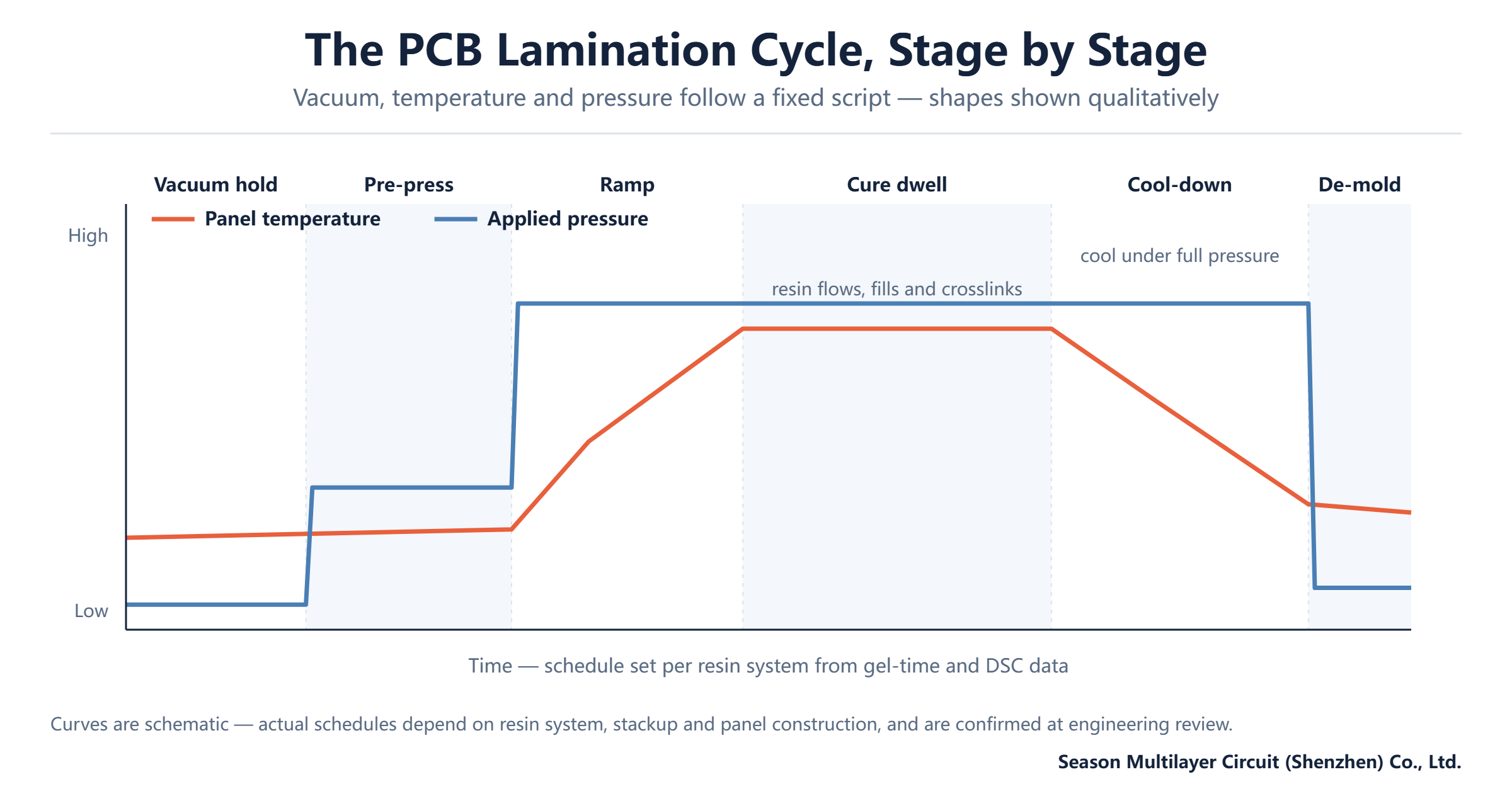
Two details worth remembering when you review a fabrication schedule. First, the cycle is a temperature-and-time recipe tied to a specific resin — moving the same stackup to a different prepreg brand usually means re-writing the schedule, not reusing it. Second, the PCB lamination cycle is written per material system, not reused across resins. Cool-down is not idle time: a board pulled out too hot or released from pressure too early can warp after it leaves the press, which shows up days later as a bow-and-twist reject.
Prepreg Flow: The Variable Buyers Never See
Prepreg is selected by resin content, flow behavior and gel time, and those three numbers decide how the PCB lamination process treats your particular stackup. Resin content sets how much epoxy is available to fill the copper pattern on the inner layers. Flow decides how far that resin travels before it gels. Gel time decides how long the press has before the chemistry commits — and the callouts themselves are standardized across the IPC laminate and prepreg specifications.
The interaction is easy to get wrong. A deep, dense copper pattern on the inner layers consumes resin as it flows — if the prepreg carries too little resin for that pattern, the cured board shows resin starvation, with thin or weak dielectric over the copper. The opposite failure is just as real: over-generous resin on a sparse pattern pushes out of the edges, and the finished board comes out thinner than the stackup called for, shifting every impedance value downward with it.
This is why a serious fabricator checks resin fill per layer pair when quoting a stackup, rather than assuming a standard prepreg build. When you send RF or controlled-impedance work to a new supplier, it is fair to ask how they choose prepreg for a given copper pattern density — the answer tells you quickly whether PCB lamination is treated as engineering or copy-paste. Our hybrid PCB stackup guide shows the same logic applied to mixed-material builds.
Temperature, Pressure and Vacuum Windows
The three press variables interact, and each failure mode has a signature. Temperature drives resin viscosity: too cold and the resin never fills the copper relief, leaving voids between layers; too hot too early and it gels before it flows, with the same voiding but a different cross-section look. Pressure must be enough to keep layers in intimate contact through the cure, but far beyond that it thins the dielectric and stresses registration.
Vacuum is the quiet third variable. Laminating without vacuum is still common for simple builds, but for HDI and fine-pitch work, vacuum assist during the early ramp pulls air and moisture out of the book before the resin seals the edges — the difference shows up measling counts and in via plating quality downstream. Moisture itself deserves respect: prepreg that has absorbed humidity from poor storage behaves unpredictably in the PCB lamination process, which is why shelf-life and cold-room handling are audited at serious factories, with resin systems tracked in the supplier’s UL recognition files.
None of these windows are universal. The PCB lamination schedule is tuned per resin system, per thickness class and per copper pattern, then locked into the press program. The takeaway for a buyer is not the numbers themselves — it is that a fabricator should be able to tell you which schedule your board runs on and why.
Registration Through the Press: Controlling Layer Shift
Between etch and drill, the stack takes a thermal excursion of well over a hundred degrees, and every material in the book expands at its own rate. Layer-to-layer registration through the press therefore has to be engineered, not hoped for: pin lamination, tooling holes and per-layer scaling factors compensate for the movement, and post-press X-ray checks verify that drilled holes landed on their pads.
Registration error in PCB lamination is unforgiving because it propagates. A layer that shifts in the press makes every drilled hole in that region land slightly off-pad — an annular-ring breakout that no plating step can repair. Tight-tolerance builds solve this with riveted or pinned stacks and by scaling inner layers to the measured expansion of the actual material lot. For the tolerance numbers behind this, see our guide to layer-to-layer registration tolerance.
Finished Thickness, Copper Balance and Warpage
Finished board thickness is decided in PCB lamination and then confirmed by measurement — but the press can only deliver what the stackup requests. The copper distribution across the layers matters as much as the dielectric heights: a stackup with heavy copper on one side and signal layers only on the other cures with unbalanced stress, and the panel relaxes into a bow or a twist as it cools.
Warpage risk grows with asymmetry, with thin cores and with large panels. Good practice is to keep copper roughly balanced about the central axis, to mirror heavy-copper layers across the thickness, and to keep the press cool-down under full pressure until the resin is well below its glass transition. Panels that will be panelized into small boards for SMT need particular attention — a flatness problem invisible at panel level becomes a feeder jam at the pick-and-place.
When you review a quote for a thick or asymmetric board, ask how the stackup handles copper balance. A fabricator who volunteers a re-balanced stackup proposal is signaling that PCB lamination is treated as engineering; one who accepts any stackup unchanged is signaling that warpage is your problem to discover later. Our 8-layer security system PCB build is a worked example of a balanced, mass-producible stackup.
Laminating Mixed Dielectrics: FR-4 With RF Layers
Many RF and high-speed boards are not laminated from a single material system. A common construction bonds one or two microwave-grade layers to standard FR-4 cores, so the RF layers get the low-loss dielectric while the digital layers keep FR-4’s cost and processability. This hybrid approach works precisely because PCB lamination is the step where the two systems meet — and it is also where the risks concentrate.
Different resin systems expand, flow and cure differently, so a hybrid book runs a schedule tuned for both, and the bond between dissimilar layers becomes the reliability-critical interface. Drilling and desmear behavior also changes: PTFE-based layers need plasma preparation that standard FR-4 does not. If your build mixes dielectrics, confirm that the fabricator has run that specific pairing before, and read our mixed-dielectric hybrid stackup walkthrough for the design-side rules.
PCB Lamination Defects: Causes and Prevention
Most lamination-linked failures fall into a short list, and each has a visible signature if you know where to look. The table below maps the common defects to their usual root causes and to the checks that catch them — useful both for interpreting a supplier’s corrective-action report and for knowing what to ask for on a first-order qualification build.
| Defect | Typical root cause | How it is caught and prevented |
|---|---|---|
| Resin starvation / thin dielectric | Prepreg resin content too low for the copper pattern | Stackup review per layer pair; cross-section on first article |
| Interlayer voids / measling | Trapped air or moisture; poor vacuum; damp prepreg | Vacuum assist, prepreg storage control, micro-section inspection |
| Delamination | Contaminated inner layers; expired prepreg; under-cure | Bake-out before press, shelf-life control, coupon pull tests |
| Layer shift | Wrong scaling for material expansion; worn tooling | Pinned or riveted stacks, post-press X-ray registration check |
| Finished thickness out of tolerance | Excess resin bleed; wrong prepreg build-up | Prepreg thickness calculation per pattern; panel thickness checks |
| Bow and twist | Unbalanced copper; early pressure release | Copper-balanced stackup review; full-pressure cool-down |
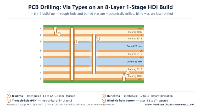
Note how many rows point back to upstream steps: a delamination can originate in dirty inner-layer handling, and a registration failure in tooling wear long before the press. The PCB lamination process is where those latent problems become permanent, which is why a first-article micro-section is the cheapest insurance you can buy on a new stackup. Downstream steps have their own failure modes — see our electroless copper deposition guide for the hole wall, and the PCB drilling process guide for hole quality.
Frequently Asked Questions
What does the PCB lamination process do?
It bonds etched inner layers, prepreg and copper foil into a single solid board under vacuum, heat and pressure. The prepreg resin melts, flows into the copper pattern and cures permanently, which fixes dielectric thickness, layer registration, finished thickness and flatness for the rest of the manufacturing chain.
How long does a lamination cycle take?
It depends on the resin system and the stackup: a cycle includes vacuum hold, pre-press, ramp, cure dwell and controlled cool-down, and the cure dwell alone is typically measured in hours for standard epoxy systems. The schedule is written from the material supplier’s gel-time and DSC data and confirmed at engineering review, so lead-time quotes should always account for it.
What is prepreg and why does it matter?
Prepreg is glass fabric pre-impregnated with partially cured resin — the bonding ply between layers. Its resin content, flow and gel time decide whether copper patterns are fully filled, whether the dielectric gap meets the stackup, and whether voids form. Choosing prepreg per layer pair, not per generic build number, is what separates a reviewed stackup from a defaulted one in PCB lamination.
What causes delamination in a multilayer PCB?
The common roots are contamination on inner layers before press, prepreg past its shelf life, moisture absorbed during storage, and under-cure in the press cycle. Delamination found at cross-section or during thermal stress testing is permanent — the affected panels are scrapped — so prevention lives in handling discipline, prepreg control and a correctly tuned schedule.
Can PCB lamination cause layer shift?
Yes. Layers expand at different rates during the press cycle, and without proper scaling and tooling the copper patterns drift relative to each other. Serious fabricators compensate with pinned or riveted stacks and per-lot scaling factors, then verify with post-press X-ray inspection before drilling.
Why is my finished board thinner than the stackup?
Excess resin bleed during the press removes material from the book, and sparse copper patterns offer little resistance to flow. The result is a thinner board and, with it, shifted impedance values. The fix is on the supplier side: prepreg selection matched to the copper pattern density and thickness verification after press, before any drilling happens.
How do I qualify a fabricator’s lamination capability?
Ask three things: how they choose prepreg for a given copper pattern, what their press schedule looks like for your material system, and what first-article inspection covers. A micro-section on the first article of a new stackup is the single most informative check — it shows resin fill, voiding, dielectric thickness and bond quality in one image.
Have Your Stackup Reviewed Before It Goes to Press
Stackup decisions are cheapest to change in a quote review and most expensive to discover at first article. Prepreg selection, copper balance and registration strategy are exactly the PCB lamination checks our engineering team runs when a new multilayer build arrives.
Submit your Gerber and stackup through our PCB manufacturing services page — from 2 to 30 layers, with press capability per material system confirmed at engineering review.