Book Appointment Now

6-Layer HDI Rearview Mirror PCB
Premium HDI PCBs — dedicated rearview mirror PCB manufacturing for smart automotive mirrors with integrated displays, touch controls, and ADAS sensor connectivity. Compact. Reliable. High-density interconnect.
Modern automotive rearview mirrors have evolved far beyond simple reflective glass. Today’s smart mirrors incorporate LCD displays, backup camera feeds, blind-spot monitoring, and touch-sensitive controls — all demanding sophisticated PCB architecture. At Season Multilayer Circuit, we manufacture 6-layer HDI rearview mirror PCBs with blind and buried vias that deliver the density, signal integrity, and thermal reliability your automotive electronics require.
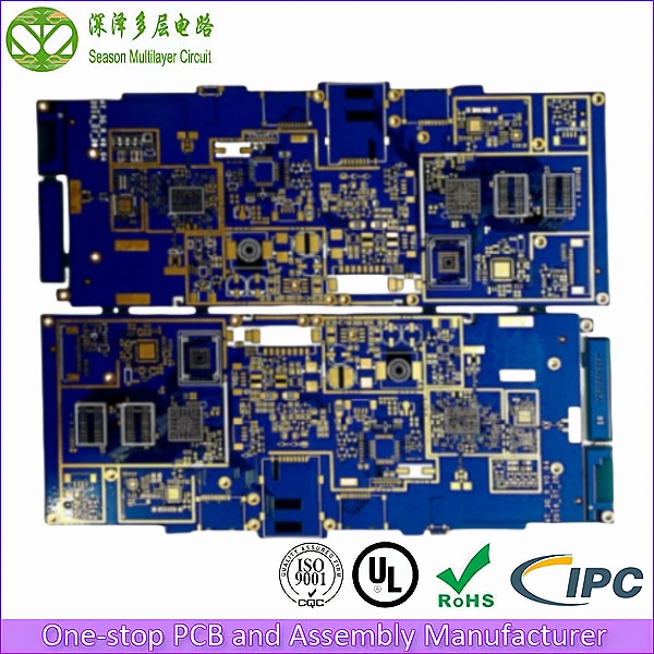
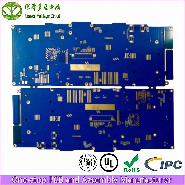
1+4+1
Layer Count
3/3 mil
Min. Trace/Space
0.10 mm
Min. Via Diameter
Tg 180
Glass Transition Temp
1-2 u”
ENIG Gold Thickness
ISO 9001:2015
ISO 14001
UL (E305905)
IPC Class 2 / Class 3
IATF 16949
RoHS
Table of Contents
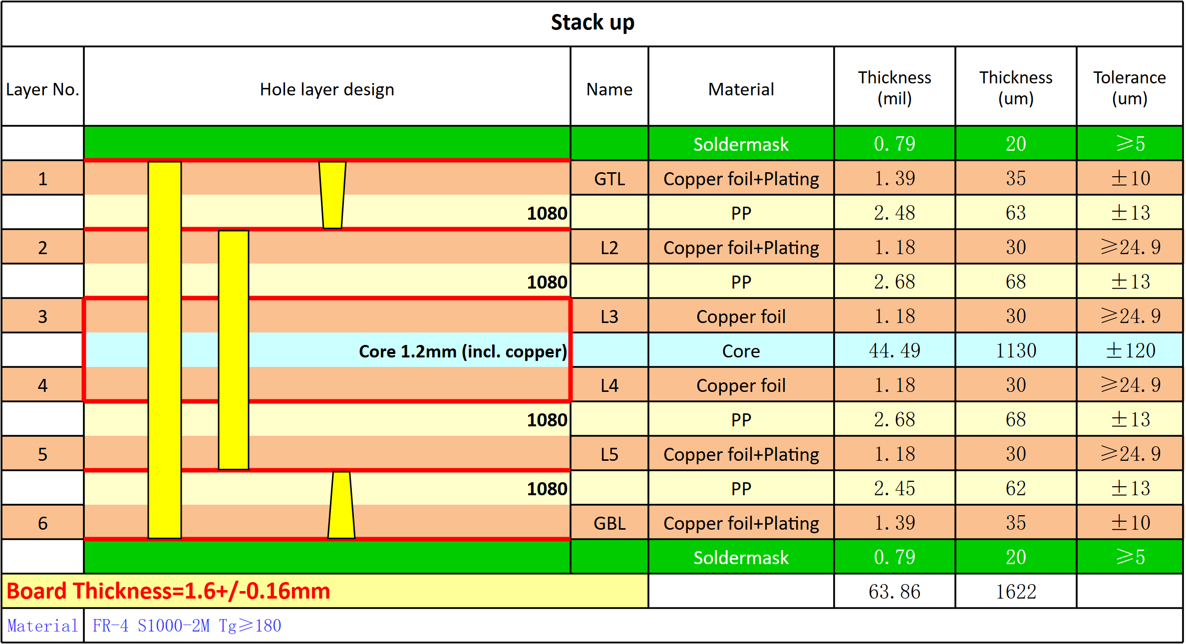
6-Layer HDI Rearview Mirror PCB Stackup Diagram
Our 6-layer HDI stackup is optimized for automotive rearview mirror applications, combining high-density interconnect technology with robust signal integrity for display driver circuits, camera interfaces, and sensor connectivity.
- Top Layer (Copper/Plated): Component placement, fine-pitch BGA, display driver ICs
- Inner Layer 2 (Ground Plane): Reference shielding for L1 and L3 signal layers
- Inner Layer 3 (Signal Layer): Controlled impedance routing for camera and display signals
- Inner Layer 4 (Power Plane): Dedicated power distribution for 12V/5V/3.3V rails
- Inner Layer 5 (Signal Layer): Secondary routing with buried via connections
- Bot Layer (Copper/Plated): Bottom routing and thermal dissipation pad
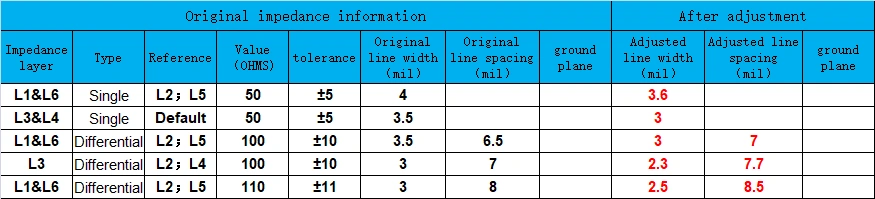
If your current trace widths and spacings fall outside strict impedance tolerance zones, our engineering team will design the optimal stackup architecture for your specific layout, making micro-adjustments to guarantee your board performs exactly as intended.
Technical Capability & Specifications
| Parameter | Specification | Advanced Capabilities |
|---|---|---|
| Layer Count | 6 Layer HDI (1+4+1) | 2-30L (Mass); 2-64L (Sample) |
| Base Material | FR-4 S1000-2M Tg 180 | High-Tg FR-4 grades; Rogers/Megtron on request |
| Board Thickness | 1.6mm | 0.2-6.4mm (Mass); 0.15-20mm (Sample) |
| Panel Size | 138x162mm | 800x600mm (Mass); 1050×610 (Sample) |
| Copper Thickness | Outer: 1 oz Inner: 1 oz | Outer: 1/3–12 oz Inner: 1/4–12 oz |
| Min Drill Size | 0.10mm (Laser) | 0.075mm (Laser Sample) |
| Min Trace Width/Spacing | 3/3 mil | 1.6/1.6 mil (Sample) |
| Blind Via | 0.10mm Laser | 0.075mm Laser (Sample) |
| Buried Via | 0.2mm Mechanical | 0.127mm (Sample) |
| Surface Finish | ENIG | HASL, OSP, Immersion Silver, Immersion Tin, ENIG, ENEPIG |
| Solder Mask | Customer-specified color | LPI (liquid photo-imageable), matte or gloss |
| Impedance Control | 50 Ohm single; 100/110 Ohm differential | Tolerance per impedance drawing (+/-5/+/-10/+/-11) |
Key Advantages of Our Rearview Mirror PCB
- Ultra-Compact Form Factor: HDI blind and buried vias enable 40% smaller board footprint compared to conventional through-hole designs, fitting perfectly within the slim profile of modern smart rearview mirrors.
- Superior Signal Integrity: Controlled impedance routing (50 ohm single-ended, 100/110 ohm differential) ensures clean transmission of high-speed display signals and camera data feeds without artifacts or latency.
- Automotive-Grade Reliability: IATF 16949 certified manufacturing with High-TG FR4 (Tg 180) substrate withstands extreme temperature cycling from -40C to 125C in automotive environments.
- Laser-Drilled Microvias: 0.10mm laser-drilled blind vias provide high-density interconnects for fine-pitch BGA packages used in display driver ICs and image signal processors.
- ENIG Surface Finish: 1-2 microinch gold over nickel provides excellent solderability and contact reliability for wire bonding and press-fit connectors in automotive applications.
Overcoming Critical Challenges in Smart Mirror Design
When sourcing HDI PCBs for automotive rearview mirror applications, electronic buyers and engineers routinely encounter three major failure points. Here is how our engineering team eliminates them:
1. Display Signal Degradation & Flickering
The Problem: Low-quality PCB stackups cause electromagnetic interference (EMI) and impedance mismatch, leading to display flickering, color distortion, and frame drops in LCD mirror displays. This is unacceptable in safety-critical automotive applications.
Our Solution: Our 6-layer HDI architecture uses tightly coupled ground planes (L2, L5) to shield high-speed display signals. Every signal layer has a dedicated ground reference, ensuring clean return paths and minimal EMI. The result: stable, artifact-free display performance even in electrically noisy automotive environments.
2. Thermal Stress in Enclosed Mirror Housings
The Problem: Smart rearview mirrors are sealed inside compact housings with no ventilation, causing rapid heat buildup from display drivers and processing chips. Internal temperatures can exceed 85C, leading to IC failure and delamination.
Our Solution: We use premium High-TG FR4 materials (Tg 180) with optimized thermal via arrays under hot components. The inner power plane (L4) acts as a thermal spreader, distributing heat evenly. For extreme environments, we offer heavy copper pours and metal-core options.
3. Space Constraints for Multi-Function Integration
The Problem: Modern smart mirrors must integrate display drivers, camera interfaces, touch controllers, and wireless modules in an extremely compact form factor. Standard PCBs simply cannot fit the required component density.
Our Solution: Our HDI technology with laser-drilled blind/buried vias enables 40% higher component density than conventional boards. Channels between components can be routed through inner layers with buried vias, eliminating the need for large through-holes that waste routing space.
Where Our Rearview Mirror PCBs Are Used
Our 6-layer HDI rearview mirror PCBs are deployed across a wide range of automotive mirror applications:
- Smart Digital Rearview Mirrors: LCD-based mirrors displaying real-time backup camera feeds with wider field of view than conventional mirrors.
- Blind-Spot Detection Mirrors: Mirrors with integrated LED indicators and side-camera connectivity for enhanced driver awareness.
- Auto-Dimming Mirrors: Electrochromic mirror assemblies with built-in light sensors and dimming control circuitry.
- ADAS Display Mirrors: Mirrors integrated with navigation overlays, speed display, and forward-collision warning alerts.
- Commercial Vehicle Camera Mirrors: Heavy-duty mirror replacement systems for trucks and buses using camera-monitor systems per UN R46.
Materials and Surface Finish Options for Your Rearview Mirror PCB
Material selection sets the ceiling on what a rearview mirror PCB can deliver over a full vehicle lifetime — thermal headroom, copper adhesion, and long-term signal stability all trace back to the laminate chosen before tooling. Our standard build uses FR-4 S1000-2M (Tg 180), a high-glass-transition laminate that keeps its mechanical properties through the -40C to 125C swings an enclosed mirror housing sees, and the same platform extends to Rogers and Megtron materials when your RF camera links need a lower-loss dielectric.
Copper follows the stackup drawing you approve: 1 oz on outer and inner layers as standard, with heavier weights available for the power rails that feed display backlights and camera modules. Laser-drilled microvias land on plated pads with 18 µm capture pads as standard, and every blind via is cross-sectioned during first-article inspection to confirm the cone is clean from surface to target layer — the discipline that keeps HDI yields stable as volumes ramp.
ENIG is our standard surface finish, giving flat, wire-bondable pads for the fine-pitch display drivers a mirror module uses, with ENEPIG, OSP, HASL, immersion silver, and immersion tin available where your assembly process calls for them. Solder mask color is customer-specified and printed in LPI ink, so the finished rearview mirror PCB matches your housing without a separate coating step.
- FR-4 S1000-2M (Tg 180) standard; Rogers/Megtron on request
- 1 oz copper standard; heavier weights for power rails
- ENIG standard; ENEPIG, OSP, HASL, immersion silver/tin available
- LPI solder mask in customer-specified color
Inside Our Rearview Mirror PCB Production Process
Every rearview mirror PCB order begins with a DFM review focused on the details that matter at HDI geometry: laser via capture pads against drill size, stacking of blind via annular rings, and impedance references against your layer assignment. Our engineers flag anything that would put the 1+4+1 stackup at risk before tooling, so corrections cost a file edit instead of a production run.
On the line, the inner core is imaged, etched, and lamination-inspected first, then the outer HDI layers are built up with 1080 prepreg and laser-drilled 0.10 mm blind vias. X-ray alignment holds layer-to-layer registration through each pressing cycle, and buried via connections between L2 and L5 are verified electrically before the outer layers of the rearview mirror PCB are drilled and plated.
After plating and patterning, every rearview mirror PCB passes 100% AOI with per-layer trace, space, and registration checks, followed by 100% electrical test by flying probe or fixture. Impedance coupons ride with each production panel, and a Polar Instruments test report ships with every batch so your incoming inspection can verify 50 ohm single-ended and 100/110 ohm differential control without building extra test boards.
For automotive programs, IATF 16949 certified processes govern traceability from laminate lot to shipment, with MES records tying each panel position to its inspection data — the documentation chain your quality team needs is generated as the board is built, not reconstructed afterward.
Design Guidelines for a Reliable Rearview Mirror PCB
HDI layouts reward a few disciplined habits. Keep laser blind vias on short reference jumps — L1 to L2 as drawn in our stackup — rather than stacking depth the 1+4+1 build was not designed for, and pair every differential camera or display link with an adjacent solid reference plane so the 100/110 ohm targets hold across the full route length. Our engineers review your layer assignment against these rules during DFM, so the stackup supports the routing style from the first revision.
Thermal layout in a rearview mirror PCB matters as much as signal layout, because an enclosed mirror housing traps heat around the display and camera electronics. Place thermal via arrays under hot components down to the L4 power plane, spread copper on the L2 ground layer around camera connectors, and keep high-current backlight rails wide enough that copper, not solder mask, defines the thermal path.
- Keep microvia capture pads at least 0.05mm larger than the drill
- Route differential pairs on layers with an unbroken adjacent reference
- Use thermal via arrays under processors and power stages
- Reserve L4 as a low-impedance power plane for display and camera rails
Where your layout pushes beyond these baselines — tighter spacing than 3/3 mil, impedance targets beyond the standard 50/100/110 ohm set, or additional depth ratios — bring them into the first conversation. Defining the extremes early lets our engineers confirm the 1+4+1 stackup absorbs them, instead of discovering conflicts after your layout is frozen.
File Preparation and Volume Scaling for Rearview Mirror PCB Programs
Clean input files keep an HDI build on schedule. We accept Gerber (RS-274X), ODB++, and IPC-2581 with Excellon drill data, plus a stackup drawing stating core and prepreg thicknesses, copper weights, via structure, and impedance targets. Marking the laser via layers and differential pairs directly in your fabrication notes removes the most common source of engineering back-and-forth.
Production runs on a 138x162mm working panel, with larger panels available for volume programs. Fiducials, breakaway rails, and test coupons are planned around your array at quotation, so a rearview mirror PCB that validates at prototype scale runs unchanged when volumes ramp — no requalification between first article and mass production. Volume pricing is confirmed at the same DFM review, so cost scales predictably with your forecast.
When your program scales, the same build moves onto 998PCB Group capacity, keeping material sourcing and process discipline consistent across facilities while you keep a single engineering point of contact. Documentation travels with every batch: laminate and finish certificates, impedance test reports, and electrical test records — a packet ready to file with your own quality system.
Our Quality Guarantee for Rearview Mirror PCBs
Automotive mirror electronics operate in harsh environments and cannot tolerate failures. We implement rigorous testing protocols on every board:
- 100% AOI Inspection: Automated Optical Inspection scans every layer for trace breaks, shorts, and alignment errors before lamination.
- 100% Electrical Testing (E-Test): Flying probe or fixture-based testing verifies continuity and isolation on every finished board.
- Controlled Impedance Testing: Dedicated Polar Instruments impedance test report with every batch documenting compliance.
- X-Ray Inspection: Available for BGA and QFN packages to verify solder joint integrity on fine-pitch display driver packages.
- Certifications: ISO 9001:2015, ISO 14001, IATF 16949, UL (E305905), RoHS compliant. IPC Class 3 available for safety-critical applications.
Why Choose Season PCB for Your Rearview Mirror PCB?
With nearly 20 years of experience in Season Multilayer Circuit has served over 8,000 global clients across automotive electronics, consumer devices, industrial equipment, and telecommunications. Our three manufacturing facilities (Shenzhen, Anhui, and Jiangxi) provide combined capacity for both rapid prototyping and high-volume mass production.
We understand that automotive mirror electronics demand zero-defect reliability. That is why every 6-layer HDI rearview mirror PCB we ship is backed by:
- Free DFM file checking before production — we catch design issues before they become manufacturing defects
- 24/7 dedicated engineering support — real engineers, not chatbots, available around the clock
- Schedule discipline — every build is planned around your project timelines
- Prototype-to-production flexibility at every project stage
- Engineering fee waivers on bulk production orders
Season PCB specializes in HDI rearview mirror PCB manufacturing for automotive display and camera applications. Our rearview mirror PCB products feature high-density interconnect technology, blind and buried vias, and reliable signal integrity. Each rearview mirror PCB meets IATF 16949 automotive standards.
Display-side builds on the same 1+4+1 HDI stackup are covered on our 6-layer HDI LED display PCB page.
For your automotive mirror PCB needs, Season PCB provides fast turnaround, competitive pricing, and IATF-certified quality. Contact us for rearview mirror PCB manufacturing today.
Our rearview mirror PCB boards comply with UL safety certifications and IPC manufacturing standards. Each rearview mirror PCB undergoes thermal stress testing and signal integrity verification. For volume production, the same stackup runs on 998PCB Group’s advanced HDI PCB lines at the group’s Shenzhen campus.
Frequently Asked Questions
Why use HDI technology for rearview mirror PCBs?
Smart rearview mirrors integrate LCD displays, camera interfaces, touch sensors, and wireless modules in an extremely compact form factor. HDI technology with laser-drilled blind and buried vias enables the high component density and fine-pitch routing required, which is impossible with conventional through-hole PCBs.
What is the minimum via size you can achieve for HDI mirror PCBs?
Our standard minimum blind via size is 0.10mm using laser drilling. For sample production, we can achieve 0.075mm laser-drilled microvias. Buried vias are typically 0.2mm mechanical, with 0.127mm available for samples.
What automotive certifications do you hold?
We are IATF 16949 certified for automotive electronics manufacturing, in addition to ISO 9001:2015, ISO 14001, UL (E305905), and RoHS compliance. IPC Class 3 manufacturing is available for safety-critical automotive applications.
What materials and stackup options are available for the 6-layer HDI mirror PCB?
The standard build is a 1+4+1 HDI stackup on FR-4 S1000-2M (Tg 180), with high-Tg FR-4 grades standard and Rogers/Megtron laminates available on request. Board thickness is 1.6mm standard (0.2-6.4mm range) with 1 oz copper on outer and inner layers. ENIG is the standard surface finish, with HASL, OSP, immersion silver, immersion tin, and ENEPIG optional. Solder mask color is customer-specified so the finished panel matches your enclosure, printed in LPI ink for 3/3 mil definition. Controlled impedance of 50 ohm single-ended and 100/110 ohm differential is supported, with tolerances defined on your impedance drawing.
How do you verify quality on automotive mirror PCBs?
Every board passes 100% AOI, which scans each layer for trace breaks, shorts, and alignment errors before lamination, plus 100% electrical testing by flying probe or fixture. A Polar Instruments impedance test report accompanies every batch, and X-Ray inspection is available for BGA and QFN packages. We are certified to ISO 9001:2015, ISO 14001, IATF 16949, UL (E305905), and RoHS, with IPC Class 3 manufacturing available for safety-critical automotive applications.
Ready to start your Rearview Mirror PCB project?
From first prototype to full production ramp, our engineering team is ready to support your project with DFM review, impedance modeling, and fast-turn fabrication.
Tel: (+86) 18681528532 | WhatsApp: +86 18681528532
E-mail: roc@season-pcb.com