Book Appointment Now

Fabricators panelize to cut waste and speed up assembly. See how PCB panelization works, which breakout method fits your board and the rules that prevent rework.
PCB Panelization: Why Boards Are Panelized and How to Design the Panel
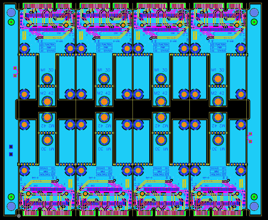
Most boards smaller than a postcard never travel through a fabrication line alone. They arrive as part of a larger production panel — several identical copies held together by rails and breakout joints — and are separated only after assembly. That practice, called PCB panelization, is one of the quietest levers on your unit price, and one of the most common sources of rework when it is designed carelessly.
This guide explains why fabricators ask for panelized Gerbers, how rails, fiducials and breakout methods work, and the design rules that keep a panel separable without stressing components. Whether your supplier panelizes for you or expects a finished panel drawing, the same few parameters decide whether the board survives depaneling cleanly.
Table of Contents
- What Is PCB Panelization?
- Why Fabricators Prefer Panelized Production
- Material Utilization and Edge Waste
- Rails, Fiducials and Tooling Holes
- V-Score, Tab-Routing and Mouse Bites
- PCB Panelization for SMT Assembly
- Panel Design Rules That Prevent Rework
- When Panelization Is Not the Right Call
- Panel Checklist Before You Release Gerbers
- FAQ
- Have Your Panel Format Reviewed With the Quote
What Is PCB Panelization?
PCB panelization is the practice of combining multiple identical — or deliberately different — circuit boards into a single production panel that moves through fabrication and assembly as one unit. The individual boards stay connected to each other and to the surrounding frame through scored lines or tab joints, and are separated in a final depaneling step after soldering.
A complete panel has three structural zones: the breakaway rails along the conveyance edges, the working copies in the middle, and the joints that connect them. The rails carry the fiducial marks and tooling holes the machines need; the joints are engineered to hold firmly during processing and release cleanly at depaneling. Getting those three zones right is the entire discipline. If your boards are very small, the fabricator may also impose a minimum panel size simply to keep the panel conveyable — the panel sizing and unit-set planning guide explains how that minimum is calculated.
Why Fabricators Prefer Panelized Production
The first reason is throughput. Plating, etching, solder-mask printing and surface-finish lines all run continuously, and every format change costs setup time and introduces a new variable. A panel lets the line process dozens of boards in a single pass, keeps the equipment at a steady operating point, and reduces the handling steps where scratches and misprints accumulate.
The second reason is consistency. Boards traveling together across a panel experience the same bath chemistry, the same press profile and the same imaging exposure, which keeps etch geometry and plating thickness uniform between copies. That uniformity is harder to guarantee when small boards are processed in scattered, isolated formats. The effect carries straight through to assembly: a panelized set feeds the SMT line as one conveyor unit instead of dozens of loose parts — the SMT assembly process guide shows how pick-and-place and reflow depend on that feed format.
Material Utilization and Edge Waste
Laminate is bought in fixed sheet sizes, and every board edge that cannot nest against another board becomes scrap. A single small board surrounded by unused laminate wastes most of the sheet; nesting copies into a panel can move material utilization by several percentage points, and at volume that difference lands directly in the per-unit price. This is why fabricators ask for panelization even when the assembly line would not strictly require it.
Utilization also interacts with board shape. Rectangular boards nest with almost no waste; boards with cut-outs, chamfers or curved outlines leave gaps that must be absorbed somewhere — either by spacing the copies further apart or by filling the panel with a different order. If your outline is irregular, discuss the nesting strategy early rather than after the quote. For buyers working with dense small-format builds such as HDI modules, the economics compound: a panel that wastes 15% of its laminate on a premium material costs far more than the same waste on standard FR-4, as covered in our HDI PCB technology guide.
Rails, Fiducials and Tooling Holes
The breakaway rail is the frame the machines actually grip. Conveyor rails clamp the outer edges, so any component or trace on those edges would be crushed — the rail exists to sacrifice that space. Rails also host the features the machines need to see and hold the panel: global fiducial marks for optical alignment and non-plated tooling holes that index the panel into fixtures across drilling, printing and testing.
Three details make rails work in practice. First, keep at least the conveyance-edge width clear of everything — the exact figure depends on the assembly line, but a few millimeters on each of the two gripped edges is the usual minimum. Second, place fiducials asymmetrically so the panel cannot be loaded rotated; two identical marks 180 degrees apart are a classic misalignment trap. Third, make tooling holes non-plated and consistent across all fabrication drawings, because drilling, routing and test fixtures all reference them.
V-Score, Tab-Routing and Mouse Bites
Breakout is the method that connects the copies and releases them later, and it is the single most consequential choice on the panel. The three common methods trade edge quality against shape freedom, and a mismatch here is a leading cause of damaged boards at depaneling.
| Breakout method | How it separates boards | Best suited for | Watch-outs |
|---|---|---|---|
| V-score (V-cut) | Narrow V-grooves cut into both surfaces; the panel snaps along the grooves after assembly | Rectangular boards with straight separation lines | Not usable where the outline has cut-outs or tabs across corners; keep parts and traces clear of the groove |
| Tab-routing | Each board routed free and held by small tab bridges, depaneled by cutting or routing the tabs | Irregular shapes, boards needing clean routed edges | Tabs leave nubs that may need smoothing; tab location sets where stress concentrates |
| Mouse bites (stamp joints) | Rows of small perforations torn or cut apart | Small rigid boards with simple outlines | Ragged edge finish; the perforation count and spacing set the break force |
One method can combine with another: a common hybrid uses V-scores on two opposite sides and tab joints on the remaining edges, which keeps straight-line snapping where the shape allows it and routed release where it does not. Whichever combination you choose, state it explicitly in the fabrication drawing — a fabricator receiving bare Gerbers will otherwise pick a default that may not suit your component placement.
PCB Panelization for SMT Assembly
On the assembly side, PCB panelization is mostly about conveyance and vision. The panel must be wide enough for the conveyor rails, narrow enough for the line’s maximum format, and rigid enough not to sag across the reflow zone. Small, thin boards that would flutter or tip over as singles stay flat and stable as a panel, which improves paste-print consistency and reduces placement failures.
Component clearance near the separation lines is the rule most often violated. Parts placed across a V-score line crack the joint under snapping stress; parts overhanging a routed tab edge collide with the depaneling blade. A practical review step is to overlay the panel drawing on the pick-and-place file and check nothing sensitive — fine-pitch connectors, ceramic capacitors, crystal cans — sits within the breakout zone. Boards destined for depaneling by router also need the routing path kept free so the bit can travel without a re-clamp step.
Panel Design Rules That Prevent Rework
Most panelization rework traces back to a handful of parameters set casually in the CAD panel file. The quick reference below collects the practices fabricators ask for most often; treat the numbers as typical guidance to confirm with your own line, since conveyor systems differ between assembly houses.
| Parameter | Common practice | Why it matters |
|---|---|---|
| Rail width on conveyance edges | A few millimeters of clear space on each gripped edge | Conveyor grip and clearance for the transport system |
| Clearance from the V-score line | Keep components, connectors and traces about 1 mm clear of the groove | Snapping stress cracks nearby joints and traces |
| Tab placement | At reinforced board points, not between fine-pitch parts | Depaneling stress concentrates at the tabs |
| Global fiducials | Three marks, asymmetrically placed | Machine-vision alignment for the whole panel |
| Tooling holes | Non-plated, identical across all drawings | Repeatable registration in drilling, printing and test fixtures |
| Board-to-board spacing | Enough room for routed channels or groove width | Too little spacing forces method changes late in CAM |
One more rule sits above the table: decide the breakout method before placing components, not after. A V-score through a connector zone cannot be fixed by clever tab placement afterward — the parts have to move, and moving parts late is how schedules slip. The failure modes that follow from ignored clearance rules are the same ones catalogued in our PCB defects and fixes guide.
When Panelization Is Not the Right Call
Panelization is a default, not a law, and a few situations argue against it. Boards with stress-sensitive components — large ceramic capacitors, glass substrates, fragile sensors — sometimes travel better as singles, because even a well-designed breakout imposes mechanical stress. Very thick or very heavy boards may exceed the conveyor or reflow load limits as a panel while passing fine as singles. And boards whose outline requires routed edges on every side gain nothing from V-score lines that would then need routing away anyway.
Quantity matters too. For a five-piece prototype run of a large board, the fabrication savings from nesting are marginal, and forcing the design into a panel can add CAM work for no return. Panelization pays back when volume multiplies the utilization and handling savings; below that threshold, let the fabricator decide the production format. If you are unsure where your order sits, the practical test is simple: ask whether the quote changes when the boards ship panelized versus singles.
Panel Checklist Before You Release Gerbers
Before sending the package, walk this short list. It covers the items that fabricators most often have to query back, and each one is cheap to fix in CAD and expensive to fix after the panel is cut. The prototype order requirements guide lists the rest of the package contents alongside these panel items.
- Breakout method stated explicitly: V-score, tab-routing, mouse bites or a hybrid
- Rails on both conveyance edges with the grip zone left clear
- Three asymmetric global fiducials and non-plated tooling holes
- Component and trace clearance verified against every separation line
- Depaneling path kept free if tab-routed boards will be router-separated
- Panel drawing supplied alongside the Gerber data — the format reference lives in the official Gerber specification
Sending a finished panel drawing with the Gerbers is the single best practice on the list. It removes the CAM engineer’s interpretation step, locks the breakout method you validated, and makes the quote comparable across suppliers. Once the order is running, the panel continues to matter: the same unit travels through the full PCB manufacturing process from imaging to shipment, and every process that touches it references the panel format you defined. For orders that include assembly, our PCB manufacturing services page describes how fabrication and SMT hand off the panel between lines.
Frequently Asked Questions
Why do fabricators panelize PCBs?
Panelization keeps automated lines running without format changes, improves material utilization by nesting copies into the laminate sheet, and gives assembly a stable conveyor unit instead of loose small boards. Copies processed together also see identical chemistry and press conditions, which improves consistency from board to board.
What is a breakaway rail in PCB panelization?
It is the sacrificial frame along the panel’s conveyance edges. Assembly machines clamp those edges, so the rail carries the fiducial marks and tooling holes while keeping real components out of the grip zone. Rails are removed at depaneling together with the breakout joints.
Which breakout method should I choose, V-score or tab-routing?
Choose V-score for rectangular boards with straight separation lines — it gives the cleanest, fastest snap. Choose tab-routing when the outline has cut-outs or needs routed edges, and mouse bites for small simple boards where edge raggedness is acceptable. Hybrid panels using both are common when the shape only partly suits scoring.
How much clearance do components need from a V-score line?
A common practice is to keep components, connectors and traces about 1 mm clear of the groove line. Snapping the panel bends the board locally along the groove, and parts inside that zone crack joints or fracture themselves. Ceramic capacitors and fine-pitch connectors deserve extra margin.
Does PCB panelization always save money?
At volume, usually yes — utilization and handling savings multiply with quantity. For a small prototype run of a large board the fabrication savings are marginal, and forcing a panel can add CAM work for no return. Ask whether the quote changes between panelized and single-board formats; that difference tells you where your order sits.
Can odd-shaped boards be panelized?
Yes, with tab-routing. Irregular outlines cannot follow a straight V-score, so each board is routed free and held by tab bridges. The trade-offs are nubs left at the tab points and stress concentration where the tabs sit, so tab placement deserves attention during layout rather than as a CAM afterthought.
What should the panel drawing I send with my Gerbers contain?
The breakout method, rail dimensions, fiducial and tooling-hole locations, board-to-board spacing, and the depaneling path if the boards will be router-separated. A complete drawing removes the CAM engineer’s interpretation step and keeps the panel you validated as the one that gets built.
Have Your Panel Format Reviewed With the Quote
Send your Gerber data with or without a panel drawing, and the engineering team will confirm the breakout method, rail format and utilization before production starts. Both panelized and single-board formats are supported from prototype through volume, with the format choice stated explicitly in the quote.
Tel: (+86) 18681528532 (WhatsApp)
E-mail: roc@season-pcb.com