Book Appointment Now

A practical guide to PCB warpage: how it is measured, what causes bow and twist, the limits that matter, and the rework that is actually safe.
PCB Warpage: Causes, Prevention and Safe Rework Options
A board that measures perfectly in CAD can still arrive on your receiving dock with a visible banana curve. PCB warpage is one of those defects that looks cosmetic and is not: a flatness problem that passes visual inspection will still jam depaneling rails, tilt fine-pitch components past their paste-alignment tolerance, and crack solder joints months after deployment. Understanding where bow and twist come from — and which of them can be fixed — saves both assembly yield and supplier relationships.
This guide covers the measurement method fabricators actually use, the flatness limits written into IPC standards, the four root causes from material CTE to warehouse humidity, and the two rework methods that are safe on bare boards. It pairs with our stackup-side guide on balanced stackup design for warpage control; this article handles everything that happens around the design.
Table of Contents
- What PCB Warpage Is and How It Is Measured
- Flatness Limits: Where 0.75% and 0.5% Come From
- Material and Stackup Causes: CTE Mismatch and Resin Content
- Design Causes: Copper Balance, Panel Size and Geometry
- How Lamination and Reflow Drive PCB Warpage
- Storage, Moisture and Mechanical Handling
- Prevention Checklist from Quote to Shipment
- Rework Options: Oven Baking and Hot-Press Flattening
- When to Rework and When to Reject
- FAQ
- Get Flatness Built Into the Spec, Not Inspected In
What PCB Warpage Is and How It Is Measured
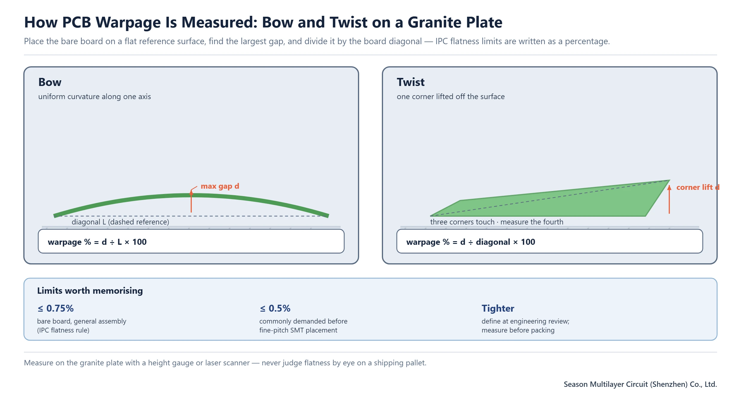
Warpage is the deviation of a board from flat when no external force is applied. The industry splits it into two modes: bow, a smooth cylindrical curvature along one axis, and twist, where one or more corners lift off the reference surface. A single panel can exhibit both at once, which is why measurement reports usually record a single worst-case figure.
The standard method is simple and hard to fake: place the bare board on a granite surface plate, find the largest gap between board and plate with a height gauge or a laser scanner, and divide that gap by the board’s diagonal length. The result is a percentage — a 2 mm gap on a 200 mm diagonal reads as 1.0%. Using the diagonal rather than the edge length is deliberate: it normalises small panels and large panels onto one comparable scale.
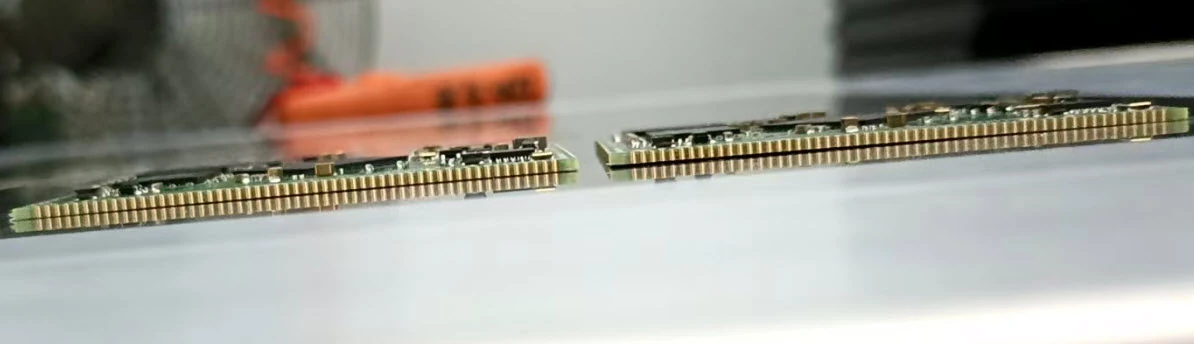
Two practical notes. First, measure before packing and again after transit if claims are disputed — boards flex differently at 50 °C inside a shipping carton than at 20 °C on the granite plate. Second, judge flatness by instrument, never by eye; a 0.6% banana curve on a large backplane is invisible across a warehouse bench but perfectly real to a vacuum nauger.
Flatness Limits: Where 0.75% and 0.5% Come From
IPC standards set the default: a maximum of 0.75% bow and twist for bare boards delivered with surface mount features in mind, tightened to 0.5% or better when fine-pitch placement is planned. The tighter value exists because pick-and-place heads and paste printers assume a flat datum — at 0.75%, the edges of a large panel sit far enough off the conveyor to skew component alignment and stencil contact.
| Application | Typical flatness spec | Why |
|---|---|---|
| Bare board, through-hole assembly | ≤ 0.75% | IPC default; wave and hand assembly tolerate curvature |
| Fine-pitch SMT placement | ≤ 0.5% | Printer and placement heads need a flat datum |
| Large panels, backplane-class | 0.5% or tighter | Diagonal grows, so absolute edge lift grows with it |
| Any critical build | Define at engineering review | Agree the limit and the measurement stage before quoting |
Note the pattern in that table: the limit is not intrinsic to the board but to what happens to it next. The IPC standards family provides the framework, and the specification sheet you agree with your fabricator should name the limit, the measurement method and the stage at which it is checked. Boards measured “at some point” are the ones that argue their way through an assembly line.
Material and Stackup Causes: CTE Mismatch and Resin Content
The root cause of most PCB warpage is stored stress: the stackup expands and contracts unevenly, and whatever asymmetry exists inside the laminate expresses itself as curvature at room temperature. Three material-level suspects dominate. First, coefficient-of-expansion mismatch — copper, glass and resin each expand at different rates, so every thermal cycle from lamination press to reflow loads the board unevenly.
Second, laminate construction quality. Variations in resin content between prepreg lots, uneven glass-cloth weave, and thickness variation across a sheet all bias the stress balance toward one side of the panel. Incoming inspection that checks thickness uniformity and resin content catches the worst offenders before they ever reach a press. Our PCB materials and laminates guide covers what a proper material data review looks like.
Third, auxiliaries that nobody thinks about: solder mask and legend inks cure with their own shrinkage and have their own expansion coefficients. A heavy mask coverage on one side and a bare second side is a classic asymmetric stress setup — the mask side shrinks more, and the board cups toward it. The fix belongs in the stackup, which is what the balanced stackup design guide treats in depth: copper distribution, layer symmetry and prepreg balance are design decisions, not process luck.
Design Causes: Copper Balance, Panel Size and Geometry
Copper is the stiffest, least-compliant layer in the stackup, and its distribution decides where stress accumulates. A board with a large solid copper pour on the top side and sparse copper underneath will cup toward the pour during etching and again during reflow. Designers mitigate this with cross-hatched pours, by balancing inner-layer copper weights layer-by-layer, and by adding dummy copper fills on light layers to restore symmetry.
Panel size and aspect ratio raise the stakes arithmetically. Flatness is measured against the diagonal, so the same absolute deformation reads worse on a 400 mm backplane than on a 100 mm module — and large panels also have more area over which process non-uniformity can integrate. Long, narrow formats are the second risk profile: a 3:1 panel bends along its long axis like a beam, while a square panel resists curvature better.
Hole fields matter more than buyers expect. A panel with dense large-diameter holes in one region and solid dielectric elsewhere carries a stiffness gradient across its width; that gradient concentrates flexural response and shows up as a bow localized at the boundary. Spreading heavy hole fields, or adding stabilization features at the transition, keeps the stiffness profile smooth.
How Lamination and Reflow Drive PCB Warpage
The press is where flatness is won or lost. Temperature ramps that are too fast cure the resin unevenly through the stack thickness — outer layers gel before inner layers reach temperature, locking a stress gradient into the panel. Pressure that is low or unevenly distributed leaves resin-starved zones that later shrink at different rates. And a cure that stops short leaves residual resin flow that relaxes during the first reflow, bending the board in the customer’s oven instead of the fabricator’s press.
Upstream and downstream steps contribute their own share. Shearing or routing with worn tooling buries mechanical stress into panel edges, which releases slowly afterward. Etching that undercuts copper unevenly across the panel shifts the copper balance the designer carefully specified. And post-etch handling — leaning panels against walls, stacking them flat in tall piles — adds creep that no press can remove later.
Reflow deserves its own paragraph because it is where warpage becomes visible to the customer. The assembly heat cycle re-melts nothing in the laminate but re-loads every interface: a board with borderline internal balance arrives within 0.75% and comes out of the oven at 0.9%. Our lamination process guide details how press parameters set the stress baseline; the design-side counterpart is keeping enough thermal margin in the stackup that one more heat cycle does not tip the balance.
Storage, Moisture and Mechanical Handling
Flat boards do not stay flat by accident between the fab and the line. Moisture is the quiet culprit: resin absorbs humidity, swells, and dries unevenly, and every absorption-drying cycle leaves a little more permanent curvature behind. Boards stored in their sealed moisture-barrier bags with desiccant keep their as-shipped flatness; boards left open on a bench in a monsoon climate do not. A bake-out before reflow — typically a few hours at modest temperature per the laminate maker’s guidance — drives off absorbed moisture without stressing the stack.
Mechanical storage damage is more visible and easier to prevent. Stacking bare boards flat in tall piles loads the bottom panels with the weight of everything above; vertical storage in racks or ESD trays keeps each panel unloaded. Transport packaging matters the same way: foam interleaving and rigid containers protect flatness as much as they protect corners, and panels that arrive rattling loose in a carton have already been flex-tested by the courier.
One rule worth writing into your incoming-inspection procedure: re-measure flatness after transit on any large or thin panel, and file the reading. When a supplier dispute arises, the differential between the shipping report and your dock measurement is the only evidence that settles who bent the board.
Prevention Checklist from Quote to Shipment
Prevention works when it is assigned to stages and owners rather than left as good intent. The sequence below runs in the order a real build does, and each item maps to a root cause from the sections above.
- At design: balance copper distribution across layers, keep stackup symmetry around the core, and flag any asymmetric mask or pour coverage for review.
- At design: prefer near-square panel outlines for large formats, or accept tighter specs for high aspect-ratio panels.
- At quotation: agree the flatness limit, the measurement method and the measurement stage in the specification sheet.
- At incoming inspection: check laminate thickness uniformity and resin content on critical builds; quarantine suspect lots.
- At fabrication: match press cure and ramp to copper weight; verify etch uniformity; avoid post-process mechanical stress.
- At packing: bag with desiccant, support panels vertically, and record the pre-ship flatness reading.
- At assembly: store sealed, bake before reflow when humidity history is unknown, and fixture large thin panels through the oven.
| Stage | Dominant cause | Highest-leverage action |
|---|---|---|
| Design | Copper asymmetry, asymmetric mask | Balance pours and layers around the core |
| Fabrication | Press cure and ramp errors | Match the press profile to copper weight |
| Storage and transit | Moisture, stack loading | Sealed bags, vertical racks, recorded readings |
| Assembly | Reflow re-loading stored stress | Bake-out and oven fixturing for large panels |
Rework Options: Oven Baking and Hot-Press Flattening
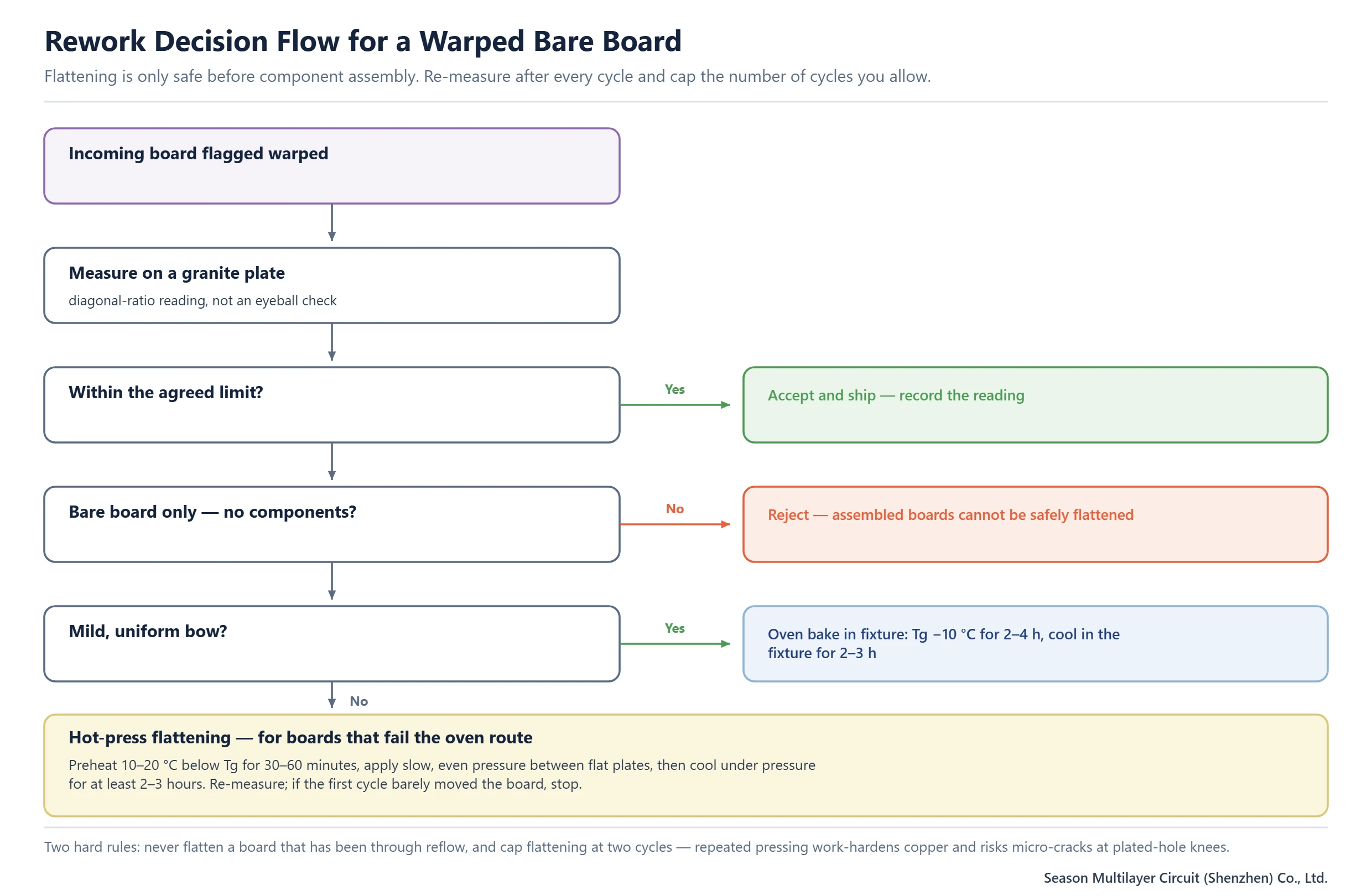
When a bare board arrives over spec, flattening is possible — with two non-negotiable conditions. First, it must be a bare board: a panel that has been through reflow carries soldered components and intermetallics that no press survives. Second, every flattening cycle is a thermal and mechanical event that the board did not sign up for, so cycles are capped and outcomes are re-measured, not assumed.
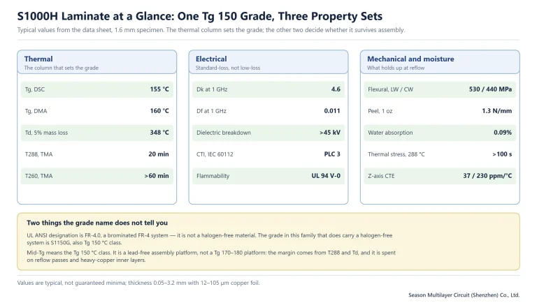
Oven baking in a fixture suits mild, uniform bow. The board is clamped flat in a heat-resistant fixture and baked slightly below the resin’s glass transition — about 10 °C under Tg, which for a Tg 150 FR-4 means roughly 140 °C — for two to four hours, then allowed to cool in the fixture over two to three hours. Slow cooling under constraint is where the flatness actually sets; pulling the board out hot discards the whole exercise.
Hot-press flattening handles deformation the oven route cannot move. The board is preheated 10–20 °C below Tg for 30–60 minutes to relax the resin, then pressed slowly and evenly between thick flat plates — with pressure-distributing layers between plate and board — and cooled under pressure for at least two to three hours. It is a genuine repair, not a recalibration, and it belongs in a fabricator’s process, not improvised on an assembly bench.
| Method | Best for | Temperature and time | Watch out for |
|---|---|---|---|
| Oven bake in fixture | Mild, uniform bow on bare boards | About Tg −10 °C for 2–4 h; cool in fixture 2–3 h | Insufficient for sharp local twist |
| Hot-press flattening | Deformation the oven route cannot move | Preheat Tg −10 to −20 °C, 30–60 min; cool under pressure ≥2–3 h | Uneven pressure creates new stress; cap at two cycles |
When to Rework and When to Reject
The decision tree in the diagram above compresses to three questions: does the board meet the agreed limit as measured, is it still bare, and is the deformation mild and uniform? A yes on all three makes oven rework routine. A board that fails, is already assembled, or shows sharp local twist goes back to the fabricator — flattening an assembled board risks component damage and solder-joint fatigue, and forcing a sharp twist flat concentrates stress exactly where plated holes are thinnest.
Two cycles is the sensible ceiling. Copper work-hardens, resin micro-cracks, and plated-hole knees accumulate damage invisibly — a board that barely improved after the first hot-press cycle is telling you its stress is structural, not superficial. Push it through a third cycle and you have manufactured a field failure with a flatness certificate.
The professional close of the loop is documentation: the incoming measurement, the rework record, and the re-measurement after. Feed all three back to the fabricator, because a recurring warpage signature on the same stackup is a design-plus-process conversation, not an incoming-inspection problem. Our PCB reliability testing overview and quality inspection report checklist cover the verification steps that catch these issues before boards reach the line.
Frequently Asked Questions
What is PCB warpage?
It is the deviation of a board from a flat plane when no force is applied, expressed as a percentage of the board diagonal. Bow is a smooth curvature along one axis; twist lifts one or more corners off the reference surface. Both modes stem from internal stress stored in the laminate.
What is the acceptable warpage limit for a PCB?
IPC sets a default maximum of 0.75% bow and twist for bare boards, commonly tightened to 0.5% or better when fine-pitch SMT placement is planned. The right figure depends on what happens to the board next, so agree the limit at engineering review and write it into the specification sheet.
How is PCB warpage measured?
Place the bare board on a granite surface plate, measure the largest gap between board and plate with a height gauge or laser scanner, and divide by the board diagonal. A 2 mm gap on a 200 mm diagonal reads as 1.0%. Measure before packing and after transit on large or thin panels.
Can a warped PCB be flattened?
Bare boards, yes, within limits. Mild uniform bow responds to oven baking in a fixture at roughly Tg −10 °C for two to four hours, cooled under the fixture. Sharper deformation needs hot-press flattening — preheat below Tg, even pressure, slow cool. Cap the effort at two cycles and re-measure after each one.
Does moisture make PCB warpage worse?
Yes. Absorbed moisture makes the resin swell, and uneven drying across the panel leaves permanent curvature behind. Store boards sealed with desiccant, bake before reflow when the humidity history is unknown, and never leave bare panels stacked open on a bench in a humid environment.
Why does copper balance reduce PCB warpage?
Copper is the stiffest, least-compliant layer in the stackup, so its distribution controls where stress accumulates. A heavy pour on one side and sparse copper on the other cups the board during etching and again at reflow. Cross-hatched pours, balanced inner-layer copper weights and dummy fills on light layers restore symmetry.
Can warpage be fixed after reflow?
No. Once components are soldered, flattening presses risk cracking solder joints and damaging parts, and reheating an assembled board past its thermal history is a reliability gamble. Reject the board to the fabricator for root-cause analysis instead — a recurring signature on the same stackup is a design and process conversation.
Get Flatness Built Into the Spec, Not Inspected In
Send your Gerber package and stackup, and we will review copper balance, panel geometry and press parameters against the flatness limit your assembly actually needs — before the build is quoted. Start from our PCB manufacturing services page, and the warpage discussion happens at engineering review instead of at receiving inspection.