Book Appointment Now

The PCB prototype requirements to check before you order: layer tiers, trace and hole minimums, impedance tolerance, acceptance class and realistic lead times.
PCB Prototype Requirements: Parameters to Confirm Before You Order

Most first-article reworks are not manufacturing failures — they are specification gaps. Layer tier, minimum trace and hole sizes, impedance tolerance, acceptance class, schedule expectations: leave any one of these out of the order and engineering review turns into a week of back-and-forth. This guide compresses the core PCB prototype requirements into a pre-order checklist, with the industry-standard reference figures behind each line item.
The bands below reflect the ranges a working quoting desk actually uses — production capability of 2–30 layers, sample-tier trace and space down to 1.8/1.8 mil, and copper weights up to 12 oz on sample builds — so you can treat the checklist as a direct proxy for the questions an engineering reviewer will ask when your Gerbers arrive. Answer them in the order file and the review usually passes in one round.
Table of Contents
- Why PCB Prototype Requirements Gaps Stall Engineering Review
- The Six Core PCB Prototype Requirements to Confirm First
- The Data Package a Complete Prototype Order Contains
- Prototype vs Production Tolerances: Confirm Them Separately
- Acceptance Standards: IPC Class 2 by Default, Class 3 on Request
- Standard Prototype Lead Times by Layer Count
- Testing and Ship-With Documents That Set the Quality Bar
- Handing Off Prototype Specs to Production Without Gaps
- FAQ
- Submit Your Gerbers for a Pre-Order Review
Why PCB Prototype Requirements Gaps Stall Engineering Review
Engineering review is not the factory being cautious — it is the point where your design intent meets process limits. A reviewer has to decide, line by line, whether the requested stack is buildable at the requested tier, and every unspecified parameter becomes a question. Five unclear parameters equal five email rounds, and each round can cost a day.
The pattern is predictable. Files arrive complete, but the order notes omit the finished thickness, or the impedance table lists target values without reference layers, or the acceptance class is never named so the reviewer has to assume one. None of these are hard questions — they are simply questions that cost a day each when asked after submission instead of before.
If you want the fuller context of what happens after the order is placed, our PCB prototyping process guide follows a board from Gerber data to first article, and the DFM analysis checklist shows what reviewers look for inside the design itself. This article stays on the order side: the parameters you should have in writing before you press submit.
The Six Core PCB Prototype Requirements to Confirm First
Six parameters decide almost every prototype review. Confirm each one in the order notes and the rest of the conversation becomes scheduling rather than engineering.
| Parameter | Industry Reference Band | What to Confirm Before Ordering |
|---|---|---|
| Layer count | 2–30 layers in production; higher counts assessed per order | Whether the build sits in the standard production tier |
| Minimum trace and space | 1.8/1.8 mil sample tier, 3/3 mil standard, 2/2 mil for HDI | Which tier the fine-pitch routing actually falls into |
| Minimum mechanical drill | 0.20 mm and up | Hole count and density in the tightest BGA region |
| Copper weight | Up to 12 oz on sample builds after engineering review | Which layers carry current and their target weight |
| BGA assembly pitch | 0.20 mm pitch as the general band | Prior experience with the package class on similar builds |
| Surface finish | ENIG, OSP, HASL and other finishes by application | Which finish suits the parts, and its storage window before SMT |
Two items are easy to overlook. First, HDI and blind/buried structures are high-tier processes: the stage count and laser via size need to be confirmed separately from the ordinary layer spec, not bundled into it. Second, surface finish affects downstream assembly. ENIG and OSP behave differently on the shelf, so if the prototype will sit for weeks before placement, state the storage period and let the finish be chosen to match. For an example of how a dense HDI order specifies these fields, see our 10-layer 2-stage HDI prototype PCB page.
The Data Package a Complete Prototype Order Contains
Incomplete files are the other half of review friction. A complete prototype package contains exactly five things, and each one prevents a specific class of questions:
- Gerber data including all drill layers, exported from the final layout revision
- Finished board thickness and copper weight per layer
- Surface finish selection, plus any solder-mask and legend requirements
- Impedance requirements, if any, with target values and reference layers named
- Quantity and the required schedule window
The impedance line deserves emphasis. If the fabricator is to simulate or verify impedance, the note must state the target value and its reference plane — a bare number like “90 ohms” cannot be checked against a stackup. For a complete data package, most quoting desks can return an itemized response within roughly one working day, which is why completeness pays for itself immediately. The Gerber format itself is maintained by Ucamco, and their Gerber specification page is the reference if you need to verify export settings.
One habit helps more than any tool: name the design revision in the file set. When a second revision shows up mid-review, both sides need to know which one is being quoted.
Prototype vs Production Tolerances: Confirm Them Separately
The same parameter can carry different standard values in the prototype tier and the production tier, and mixing the two in one question is a reliable way to get a contradictory answer. The three rows below cover the gaps that cause the most confusion.
| Parameter | Prototype Tier | Production Tier |
|---|---|---|
| Impedance tolerance | ±5% | ±8% |
| Trace and space | 1.8/1.8 mil sample tier | 3/3 mil standard, 2/2 mil for HDI |
| Acceptance class | Agreed at quoting | Class 2 by default, Class 3 by request |
Impedance tolerance is the classic case. Prototypes are typically held to ±5% because samples exist to validate a design, while production settles at ±8% once the process is characterized. Write the tolerance into the stackup requirement and have the test coupon fabricated with the panel — a coupon built later verifies nothing. Our impedance measurement guide explains how TDR and coupon testing close that loop.
Trace and space follows the same logic in reverse: a prototype may justify the finest tier to prove a design, but the production release should use the widest rule the design tolerates, because yield and cost both live there. Confirm both tiers explicitly so nobody carries a prototype-grade spec into a volume quote.
Acceptance Standards: IPC Class 2 by Default, Class 3 on Request
Acceptance criteria decide what counts as a good board, and they should be named in the quotation, not discovered at incoming inspection. The industry baseline is IPC-A-600 (visual acceptance) together with IPC-6012 (performance specification). Class 2 is the default for commercial and industrial electronics; Class 3 is the high-reliability tier used where failure is expensive, and it tightens annular ring, plating and inspection requirements across the board.
The practical advice is asymmetric. Do not pay Class 3 pricing for a board that will live in a controlled enclosure — but if the product genuinely needs Class 3, say so at quoting, because retro-fitting the requirement after the first article means re-qualifying the build. Our IPC-A-600 Class 3 guide details what the class changes in practice, and the IPC standards overview maps where each document sits in the acceptance framework.
Whatever class you choose, put the class designation and the governing document revision into the purchase specification. That single line converts “good quality” from an opinion into a checkable statement.
Standard Prototype Lead Times by Layer Count
Schedule expectations should follow the same discipline as tolerances: ask for the standard window first, then discuss compression if the project needs it. A clear written statement of PCB prototype requirements is what keeps that conversation short. The table below shows typical standard windows for conventional multilayer prototypes; every figure is confirmed at engineering review against the actual process stack.
| Build | Typical Standard Window | Note |
|---|---|---|
| 4-layer | about 5 working days | Conventional stack, no special processes |
| 6-layer | about 7 working days | Adds an inner-layer cycle |
| 8-layer | about 9 working days | Common for control and interface boards |
| 10–12 layer | about 11–12 working days | Often pairs with impedance control |
| 16–30 layer | about 14–16 working days | High-layer builds reviewed per structure |
Three scheduling notes that save arguments later. First, review time is part of the schedule: when parameters are unclear, the review itself can consume more than a day before fabrication even starts — which is exactly what the checklist earlier in this article prevents. Second, special processes such as heavy copper, HDI stages and resin plugging change the window and are assessed per order, and genuinely compressed schedules are quoted against the real process stack rather than promised reflexively. Third, ask the supplier to confirm the window in writing with the quotation, so schedule and price are agreed in the same document. For the factory-side view of what those windows contain, see our manufacturing capability page.
Testing and Ship-With Documents That Set the Quality Bar
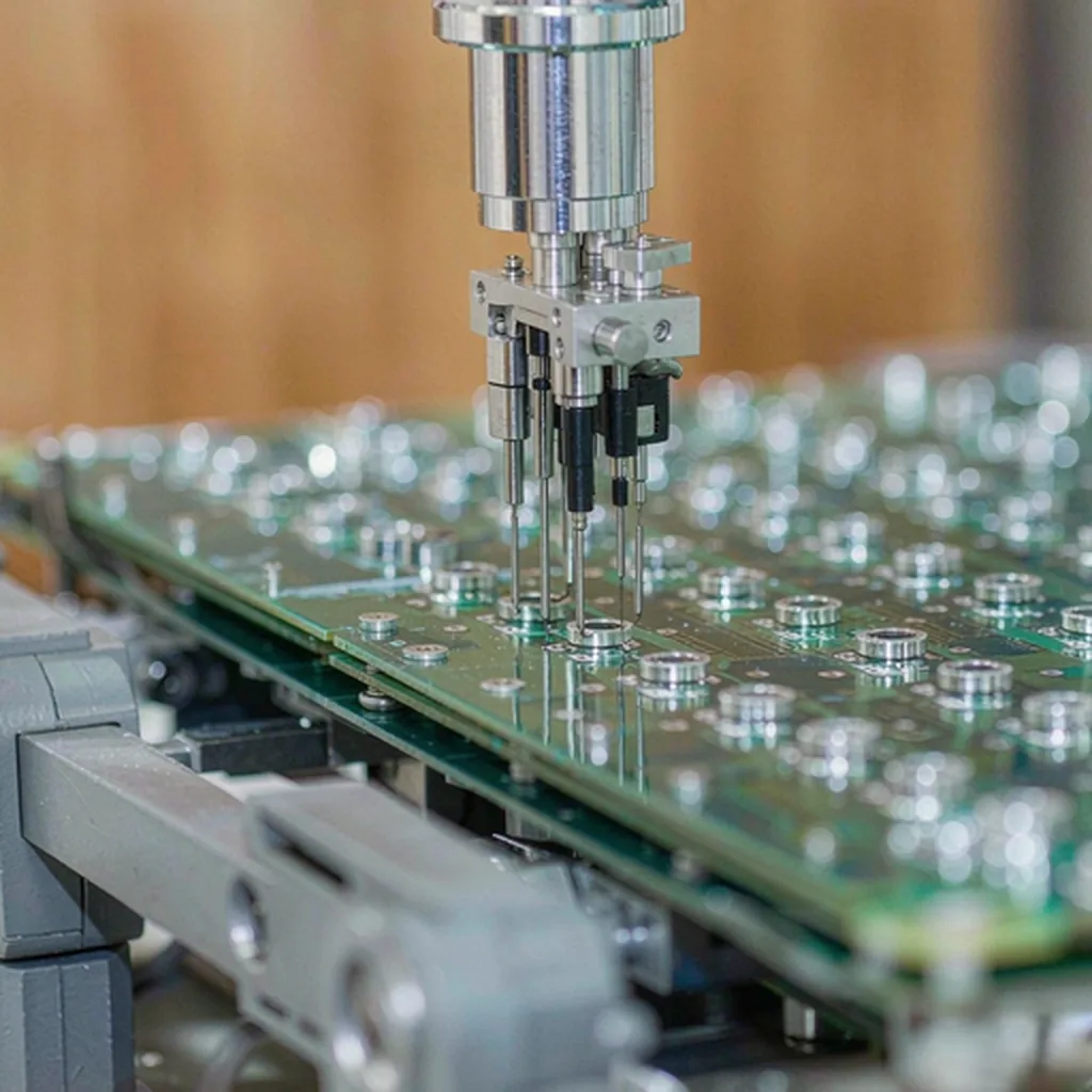
Prototype quality is not a matter of trusting the brochure — it is verifiable from two things: the routine test line and the documents that ship with the boards. A capable prototype line runs 100% electrical test (flying probe or fixture bed), automated optical inspection, X-ray on dense via and BGA regions, and TDR verification on impedance-controlled builds, with cross-section analysis retained per batch.
The ship-with documents are the part buyers forget to demand. At minimum: the electrical test report and the visual inspection record. On high-reliability orders, add cross-section photographs and the impedance test report for the coupon from your actual panel. Asking for these at the prototype stage costs nothing and sets the baseline — once the requirement exists, the production order inherits it automatically.
If a quote looks meaningfully cheaper than the others, this is the section to probe. The cheapest way to cut prototype cost is to shorten the test line, and the difference only becomes visible when a field failure traces back to a net that was never probed.
Handing Off Prototype Specs to Production Without Gaps
When the prototype passes, the temptation is to forward the same files to production and move on. The better move is to package what the prototype proved: the agreed stackup, the measured impedance values from the coupon, the acceptance class, and any engineering-review dispositions that were made along the way. That package is the specification the production order should reference.
Two tier changes need explicit confirmation in the handoff. Impedance tolerance moves from the prototype ±5% band to the production ±8% band, and the trace-and-space tier should be re-widened to whatever the design genuinely tolerates rather than the finest rule the prototype used. Both changes are normal — the mistake is letting them happen silently.
Finally, remember that batch pricing follows different logic from prototype pricing, so the production quote should be re-derived from the production spec, not extrapolated from the prototype invoice. If you are choosing a production partner separately, our manufacturer selection checklist covers the five dimensions worth verifying before the volume order.
Frequently Asked Questions
What are the core PCB prototype requirements to confirm before ordering?
Six: layer tier (2–30 layers in production, higher assessed per order), minimum trace and space (1.8/1.8 mil sample tier), minimum mechanical drill (0.20 mm and up), copper weight per layer, surface finish and its storage window, and impedance requirements with reference layers named. Confirming these six in writing prevents most engineering-review round trips.
What acceptance standard applies to prototype PCBs?
The industry baseline is IPC-A-600 with IPC-6012. Class 2 is the default for commercial and industrial builds; Class 3 is the high-reliability tier and should be requested at quoting so inspection and plating requirements are set from the start. Name the class and document revision in the purchase specification.
What files does a complete prototype order need?
Gerber data including all drill layers, finished thickness and copper weight per layer, surface finish selection, impedance requirements with target values and reference planes, and quantity with the schedule window. The most common gaps are missing drill files, unspecified thickness and impedance numbers without reference layers.
What is the minimum trace width for a PCB prototype?
Sample-tier capability runs down to 1.8/1.8 mil, the standard production rule is 3/3 mil, and HDI processes reach 2/2 mil. Finer is not better: use the widest rule the design tolerates, because tighter tiers raise both review complexity and cost.
Is impedance tolerance tighter on prototypes than production?
Yes. The common convention is ±5% on prototype builds and ±8% in production, because samples exist to validate a design while production runs on a characterized process. Write the tolerance into the stackup requirement and build the test coupon with the panel.
How long does a multilayer PCB prototype take?
Typical standard windows run about 5 working days for a 4-layer build, about 7 for 6 layers, about 9 for 8 layers, 11–12 for 10–12 layers and 14–16 for 16–30 layers, all confirmed at engineering review. Review time counts toward the schedule, and special processes are assessed per order.
What should I archive before moving a prototype to production?
The agreed stackup, the measured impedance values from the coupon, the acceptance class, and every engineering-review disposition made during the prototype. Confirm the production-tier changes explicitly — impedance tolerance relaxing to ±8% and the trace-and-space tier re-widened — so nothing shifts silently between the two tiers.
Submit Your Gerbers for a Pre-Order Review
Send your Gerber package with the layer count, copper weight, impedance targets and schedule window, and our engineering team will check it against the six core parameters before quoting — complete data packages typically receive an itemized response within roughly one working day. 998 PCB Group manufactures 2–30 layers with heavy copper and HDI assessed per order. Start through our PCB manufacturing services page.