Book Appointment Now

An automotive electronics PCB is specified by its qualification envelope, not its schematic: laminate grade, copper weight, via reliability and audit items.
Automotive Electronics PCB: Materials, Stackup and Process Rules
Most automotive electronics PCB programs fail review for reasons that have nothing to do with the schematic. A laminate grade is picked for cost rather than for the thermal excursion the assembly actually sees. Copper weight is carried over from a consumer board that never had to feed a connector at full load. A via stack passes the first reflow and cracks two years later. This guide is written for the people who have to sign off the fabrication drawing: hardware engineers, sourcing engineers and program managers who need to know which requirements change once a board has to live inside a vehicle.
Every section below is written as a decision rather than a definition. Which laminate grade belongs in which temperature zone, how copper weight follows current instead of habit, where a 1-Stage HDI build is enough and where it is not, which surface finish survives humidity and sulfur, and what to inspect in a supplier’s process before releasing volume. Numbers are the ones we quote in engineering review, and the ones you can hold a supplier to.
Table of Contents
- What Makes an Automotive Electronics PCB Different From a Consumer Board
- Operating Temperature Decides the Laminate Grade
- Reading Tg, Td and T260/T288 Correctly
- Copper Weight, Current Carrying and Heat Spreading
- Stackup Choices for Automotive Electronics PCB Builds
- Via Design and HDI Stage Count Under Thermal Cycling
- Surface Finish and Corrosion Resistance
- EMC: Reference Planes, Grounding and Shielding
- Process Controls and Traceability Worth Auditing
- The Documentation Package to Request With the First Article
- FAQ
- Send Your Automotive Stackup for a Manufacturing Review
What Makes an Automotive Electronics PCB Different From a Consumer Board
The circuit may be identical; the qualification envelope is not. A consumer board is judged over a two to three year service life in a controlled environment. A vehicle module is judged over ten to fifteen years of thermal excursion, vibration, humidity, salt spray, contamination and thermal cycling from repeated power-up. The economic logic is also inverted: the board is a small fraction of the module cost, while a field replacement is a warranty event plus a dealership labour charge. That asymmetry is why an automotive electronics PCB is specified with process requirements written directly on the fabrication drawing instead of being left to the fabricator’s default process.
In practice the difference shows up in five places: laminate grade and its thermal limits, copper weight relative to current, stackup symmetry and reference plane integrity, via construction, and surface finish. Everything else — solder mask, legend, routing rules — follows from those five. If a quote arrives without a stated Tg, a stated copper weight per layer and a stated finish thickness, the specification is not finished yet.
The most common gap we see is a board that was designed for a cabin product and then re-purposed for a body-control or powertrain-adjacent location. Standard FR-4 at 1 oz with a hot-air solder levelled finish will run in a dashboard module. Move the same board next to a heat source and the failure mode changes from ‘works’ to ‘works until the third summer’.
Operating Temperature Decides the Laminate Grade
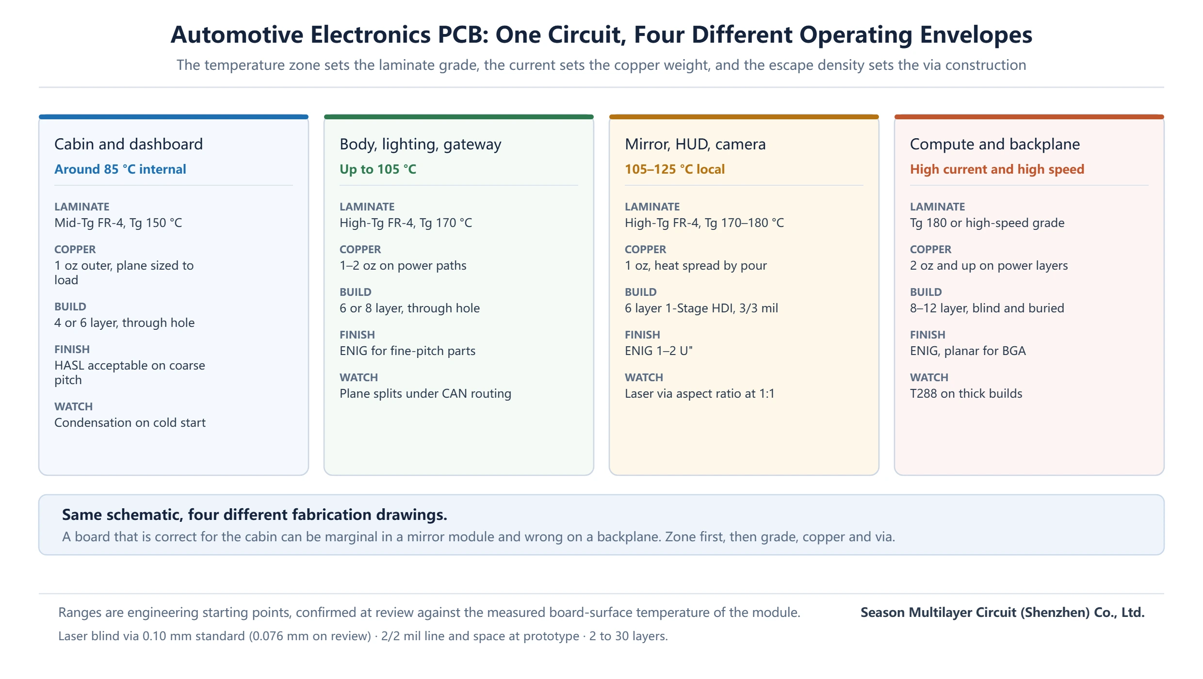
Start from the temperature an automotive electronics PCB actually sees at its surface, not from the ambient the marketing specification quotes. A cabin module may sit at 85 °C internally; a module mounted near a heat source can see 105–125 °C locally and a much higher excursion during a soak-after-key-off event. Add the reflow profile the assembly will survive during build, and the laminate has to satisfy two different thermal requirements: a working temperature and a process temperature. Our laminate selection guide covers the electrical side of the same decision for high-speed designs.
| Laminate grade | Tg | Thermal position | Halogen | Where it is specified |
|---|---|---|---|---|
| S1000H | 150 °C | Mid-Tg FR-4 | Brominated | Cabin modules, short thermal exposure, cost-sensitive builds |
| S1170G | 170 °C | Tg 170 FR-4 grade | Brominated | Mirror, HUD and body modules near a heat source |
| S1000-2M | 180 °C | Tg 180 FR-4 grade | Brominated | Thick multi-layer builds and repeated reflow assembly |
| S1150G | ≥150 °C | Halogen-free FR-4 | Halogen-free | Programs with a halogen-free material mandate |
Two notes on reading that table. First, Tg is a transition point, not a maximum working temperature: a Tg 150 laminate does not stop working at 150 °C, but its z-axis expansion and mechanical modulus change sharply there, which is what drives plated hole stress. Second, the halogen column matters for procurement rather than performance — several programs now mandate halogen-free material as a procurement requirement, and that requirement decides the grade before any thermal argument begins.
For designs where tracking resistance is a limiting factor — high-voltage connector areas, charger inputs, wet-zone modules — specify Comparative Tracking Index along with the laminate. CTI is graded in performance level classes and measured under IEC 60112; a PLC 3 material is the common baseline and PLC 4 or better is a specific ask you should write down rather than assume.
Reading Tg, Td and T260/T288 Correctly
Data sheets quote Tg by DSC and by DMA, and the two numbers typically differ by about 5 °C. On a high-Tg grade you may see 180 °C by DSC and 185 °C by DMA for the same material. Neither is wrong; comparing a DSC figure from one supplier against a DMA figure from another is how a material ends up looking better than it is. Specify the method on the drawing so the incoming certificate and the data sheet speak the same language.
Td — decomposition temperature, measured by thermogravimetric analysis at 5% weight loss — sits far above Tg and describes how the resin behaves when it is pushed. A Tg 180 FR-4 typically decomposes around 355 °C. That headroom is what makes lead-free reflow and repeated assembly cycles safe, and it is also the number that separates a genuine high-Tg product from a filled standard grade.
T260 and T288 are time-to-delamination at fixed temperature, and they are the most under-specified numbers in automotive work. Thick boards, heavy copper and large panel utilisation all raise the risk that the laminate delaminates during assembly or repair rework. Requiring T288 of at least 30 minutes and T260 above 60 minutes removes most of that risk before it reaches your line, and costs nothing to state.
Copper Weight, Current Carrying and Heat Spreading
Copper weight on an automotive electronics PCB follows current, temperature rise and the copper’s ability to dump heat into the rest of the board. A 1 oz (35 µm) outer layer carrying a few hundred milliamps of logic current is generous; the same 1 oz layer feeding a motor driver or a connector that hands current to another module is often the thermal bottleneck. Our heavy copper design rules cover the 2 oz to 6 oz range, which is where most power-side automotive work lands.
Three practical rules survive contact with production. First, size inner-layer power planes for the current they carry, not for the net class they were assigned: inner copper on a 1.6 mm six-layer board is often the hottest copper in the stack. Second, keep the thermal path continuous — a pour that is interrupted by a plane split or a mounting hole ring delivers far less than its area suggests. Third, treat connector escape routing as a current path with its own bottleneck, because that is where most local heating is actually measured.
Surface finish thickness also belongs in this conversation. A finish that is too thin over heavy copper exposes IMC growth and solderability risk on the joints that carry the current, while one that is too thick embrittles fine-pitch joints. On the builds we quote for automotive use, 1–2 U” of gold over electroless nickel is the usual request, and it holds up across the finish-thickness checks in first-article inspection.
Stackup Choices for Automotive Electronics PCB Builds
Layer count on an automotive electronics PCB is set by routing density and by how many clean reference planes the design needs, not by a preference for a round number. In automotive work the second driver is often the strongest: a design that needs two solid reference planes for CAN, camera or radar interfaces cannot be squeezed into four layers without paying for it in EMC margin.
| Build | Typical function | Via construction | Min line / space | Relative cost |
|---|---|---|---|---|
| 4-layer | Sensor, switch and small body modules | Through hole only | 4/4 mil | Baseline |
| 6-layer | Body control, lighting, gateway sub-boards | Through hole only | 3.5/3.5 mil | +20–35% |
| 6-layer 1-Stage HDI | Mirror, HUD and compact camera modules | Laser blind via + through hole | 3/3 mil | +45–70% |
| 8-layer | Domain controllers, multi-interface gateways | Through hole, some blind/buried | 3/3 mil | +60–90% |
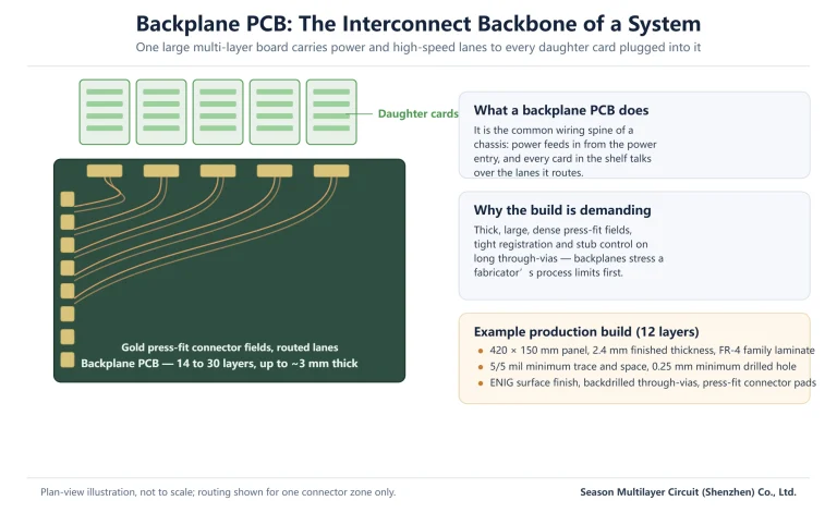
| 12-layer high-speed backplane | Compute and sensor-fusion backplanes | Blind, buried and through hole | 2.5/2.5 mil | +150% and up |
Two build rules keep the stack manufacturable. Keep it symmetrical around the centre line in both copper weight and dielectric thickness, because an asymmetric stack warps during lamination and warp is a handling problem long before it is an electrical one — the underlying mechanics are covered in our stackup design rules. And put every high-speed layer next to a continuous plane, then check the plane for splits under the routing rather than at the schematic stage.
When the module is a mirror, HUD or compact camera board, the package pitch usually forces HDI. A representative build we run is a 6-layer 1-Stage HDI at 1.6 mm with 0.20 mm through holes, 0.10–0.20 mm laser blind vias, 3/3 mil traces and 1–2 U” ENIG — the same class of build as our 6-layer HDI automotive HUD board. Where the module needs a wider interface count, the 12-layer automotive high-speed backplane build is the other end of the range.
Via Design and HDI Stage Count Under Thermal Cycling
On an automotive electronics PCB, plated hole failures are mechanical, not electrical. Above Tg the z-axis expansion of the laminate jumps from roughly 40–50 ppm/°C to around 200 ppm/°C, and the copper barrel has to absorb that movement over every thermal cycle. The two variables you control are the strain per cycle and the barrel quality: a thinner board, a shorter hole and a well-plated barrel each buy margin.
Aspect ratio is the first limit to check. On our builds we work to a maximum around 10:1 for through holes, with 0.20 mm as the standard mechanical drill and 0.10 mm as the standard laser blind via, at roughly 1:1 blind-via aspect ratio. The plating and drilling limits behind those numbers are set out in our aspect ratio guide. If a design needs a 0.15 mm hole through a 2.0 mm board, the conversation should be about redesigning the stack, not about pushing the drill.
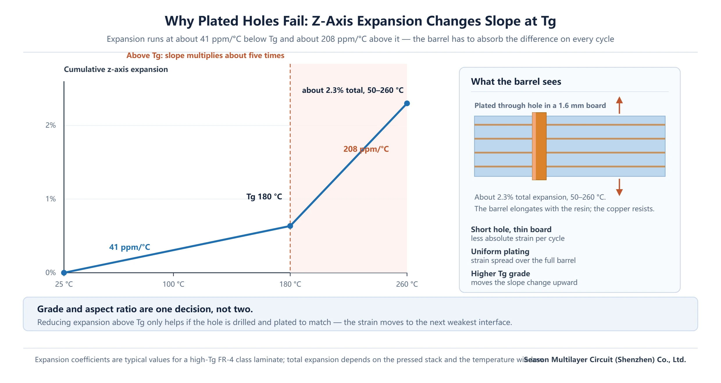
Stage count is a routing answer, not a status symbol. A single build-up layer per face (1-Stage) covers most mirror, HUD and camera modules; a second stage is justified when the BGA pitch and escape density genuinely run out of room on the first layer. Each additional stage adds two more lamination and laser drill cycles, and it also adds interfaces between stacked vias — which is where z-axis stress concentrates. The construction differences are summarised in our HDI technology guide.
Surface Finish and Corrosion Resistance
The environment an automotive electronics PCB has to survive adds sulfur, humidity and salt to the list of things a finish has to resist. Hot-air solder levelling is the cheapest option and still common on cabin boards, but its coplanarity is poor for fine-pitch parts and it offers no real protection against tarnish in a sulfur-bearing atmosphere. Electroless nickel immersion gold gives a planar surface for fine-pitch assembly plus a barrier that survives humidity, and it is the finish we see specified most often on camera, radar and mirror modules.
Immersion silver and OSP are viable where cost and reflow windows dominate, but both require tighter process control on the assembly side: OSP has a limited number of reflow passes and immersion silver tarnishes if storage and packing are loose. Whatever the choice, write the thickness on the drawing and verify it on the certificate — an ENIG callout without a thickness figure is not a specification.
Flammability and safety recognition belong here too. Laminate flammability is measured to UL 94 and the finished board carries a UL 796 recognition tied to the material and construction actually used. If a program requires a specific UL file on the finished article, say so before the material is ordered, because changing laminate grade afterwards invalidates the construction that was recognised.
EMC: Reference Planes, Grounding and Shielding
On an automotive electronics PCB, most EMC problems start on the board rather than in the enclosure. The dominant cause is a return current forced to detour: a signal crosses a plane split, the return path loops around the split, and the loop becomes an antenna. Keeping every high-speed net over one continuous reference plane, and stitching the planes together with vias on a regular grid, removes that mechanism before any shielding is added.
Ground architecture comes second. Separate signal and power ground returns meet at one defined point, usually at the connector or the regulator, and the tie should be a deliberate copper shape rather than an accidental overlap. Where a module has a chassis connection, treat the mounting pads as part of the ground plan: a mounting ring that is isolated from the plane by a slot is a common and expensive mistake on body modules.
Shielding is the last tool, not the first. A can footprint needs a continuous ground fence with enough vias to keep the fence at the same potential — a fence with gaps behaves as a slot antenna. If a design needs a shield can, plan the fence and the keep-out at layout, because retrofitting one usually means another board spin.
Process Controls and Traceability Worth Auditing
The fabrication drawing defines what the board is; the process defines what it will be in year eight. Before releasing volume, audit the controls that actually correlate with field failures rather than the ones that are easy to present. Panel traceability and material lot records matter more than a certificate wall, because they are what make a containment possible when a single lot behaves badly.
| Control point | Question to ask | Evidence you should receive |
|---|---|---|
| Laminate incoming | Is every lot verified against the ordered grade, with method stated? | Lot certificate with Tg method, T260/T288 and thickness |
| Drilling | What is the drill wear and hit-count policy per panel? | Drill log per tool, hole position report |
| Plating | How is barrel thickness verified on the smallest hole? | Microsection of the minimum hole, plating thickness map |
| Imaging and etching | How is line width held across the panel? | AOI report, first-article dimensional report |
| Lamination | What is the press cycle and how is registration verified? | Press recipe, layer-to-layer registration measurement |
| Electrical test | Is the test on the finished board 100% or sampled? | Flying probe or fixture test report, continuity and isolation limits |
| Final inspection | Which acceptance class is applied, and by whom? | IPC-A-600 inspection record per lot |
Acceptance class is the single most useful lever in that table. Many programs default to Class 2 because it is what the fabricator quotes, then discover that voiding, annular ring and plating thickness criteria in IPC Class 3 are what they actually need for a high-reliability module. Class 3 costs more and narrows the supplier pool, so make it a deliberate decision tied to the module’s criticality rather than a line item added at the end.
Quality system coverage is the other half. A supplier working to IATF 16949 has the change-control and traceability structure that automotive programs expect; it does not replace board-level inspection, but it does mean a laminate substitution cannot happen silently between lots. If your program requires it, ask for the certificate scope and confirm that the plant producing your boards is inside that scope. Our own capability envelope and equipment list are summarised on the manufacturing capability page.
The Documentation Package to Request With the First Article
First-article approval is where an automotive electronics PCB program either gains a baseline or inherits a decade of ambiguity. Ask for a package, not a board. The list below is the one we send by default, and it is short enough that a supplier without a working quality system cannot produce it.
- Fabrication drawing with laminate grade, Tg method, copper weight per layer and finish thickness stated numerically
- Stackup table with dielectric thickness and material per layer, confirmed against the pressed build
- Microsection of the minimum through hole and, on HDI builds, of the laser blind via
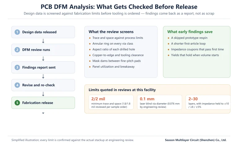
- Impedance coupon report where controlled impedance is specified, against the ±10% or tighter tolerance on the drawing
- Solder mask and finish thickness measurements, plus the plating thickness map for the panel
- Electrical test report: continuity, isolation and the test limits applied
- Material lot certificates and the traceability link from lot to panel to shipping carton
- Inspection record stating the acceptance class applied and the operator qualification behind it
Keep that package with the program, not with the purchase order. When a second source is added or a laminate grade is substituted two years later, the package is what makes the comparison meaningful — and it is the difference between a controlled change and an unexplained shift in field returns.
Frequently Asked Questions
What is the difference between an automotive electronics PCB and a standard FR-4 board?
The circuit can be identical; the specification is not. An automotive board is specified with a laminate grade tied to a temperature zone, copper weight tied to current, a symmetrical stackup with continuous reference planes, controlled via construction and a stated finish thickness. It also carries lot traceability and an acceptance class chosen deliberately, typically IPC Class 3 for safety-related modules.
Which Tg should I specify for an automotive electronics PCB?
Match it to the temperature the board surface sees. Cabin modules commonly run on a mid-Tg grade at Tg 150 °C. Modules near a heat source, such as mirror and HUD boards, usually specify Tg 170 °C, and thick or repeatedly reflowed assemblies move to Tg 180 °C. State the measurement method, because DSC and DMA readings on the same material differ by about 5 °C.
Can a 1-Stage HDI build meet automotive requirements?
Yes, and it is the most common HDI construction for mirror, HUD and compact camera modules. A 6-layer 1-Stage build with 0.10 mm laser blind vias, 0.20 mm through holes and 3/3 mil traces covers most of that class of design. A second stage is added only when BGA pitch and escape density genuinely exceed what the first build-up layer can route.
What copper weight is typical for automotive power boards?
Most logic-heavy modules run 1 oz on outer layers, with inner planes sized to the current they actually carry. Power-side boards feeding motors, lighting strings or connectors commonly move to 2 oz, and higher where local heating is measured. The limiting factor is usually the escape routing at the connector, not the plane area.
Which surface finish is best for automotive PCBs?
Electroless nickel immersion gold at 1–2 U” is the usual choice where fine-pitch assembly, humidity and sulfur exposure all apply, because it is planar and forms a barrier over the copper. Hot-air solder levelling remains acceptable on cabin boards with coarser pitch, and OSP or immersion silver are viable where reflow passes and storage conditions are tightly controlled.
How long does an automotive PCB prototype take?
As an order of magnitude, an 8–10 layer 2-Stage HDI prototype typically runs 17–18 working days, and simpler 4- or 6-layer through-hole builds are faster. HDI stage count, heavy copper, impedance control and first-article documentation all extend the schedule, so the exact date is confirmed at engineering review against the released stackup.
Do I need IPC Class 3 for automotive boards?
Not automatically, but it is the right default for safety-related and long-service modules. Class 3 tightens voiding, annular ring and plating thickness criteria and narrows the supplier pool. Decide it per module based on criticality and field-replacement cost, and state the class on the drawing so final inspection and the certificate agree.
Send Your Automotive Stackup for a Manufacturing Review
If you have a released stackup and a Gerber set, send both. We review laminate grade against the temperature zone, copper weight against current, via construction against aspect ratio and finish against the assembly process, then return the manufacturability notes with the quoted build. Where the design is not settled yet, the review usually saves a board spin rather than a day of build time.
Automotive builds are quoted through our PCB manufacturing services, from 2 to 30 layers with 1-Stage, 2-Stage and Any-layer HDI, laser blind vias from 0.10 mm and 2/2 mil line and space at prototype. A 6-layer automotive prototype is a common starting point for a first evaluation build.