Book Appointment Now

Open vias inside BGA pads wick solder. See how resin-filled, copper-capped via-in-pad technology keeps fine-pitch pads flat and solderable.
Via-in-Pad Technology for HDI and BGA Boards: Process and Rules
Fine-pitch BGAs have a way of exposing the weakest assumption in a layout: that every via can sit somewhere else. When escape channels run out, the via has to move inside the pad itself, and that is where via-in-pad technology enters. Placing a drilled, filled and plated-shut via directly under a component pad reclaims routing space that traditional fan-out wastes – but only if the filling and capping process is controlled well enough to keep the pad flat and solderable. This guide explains how the process actually works: the three via-in-pad variants and where each fits, the manufacturing sequence from drill to copper cap, the soldering risks that make unfilled pad vias dangerous, and the design rules that keep the build producible. Values are typical industry practice or our own process capability, confirmed at engineering review for every stackup.
Table of Contents
- What Via-in-Pad Technology Means in PCB Design
- Three Via-in-Pad Process Types Compared
- BGA Escape Routing and Fine-Pitch Benefits
- The Manufacturing Sequence Step by Step
- Solder Wicking, Voids and Other Failure Modes
- Design Rules That Keep Via-in-Pad Buildable
- Cost Impact and Where to Specify It Selectively
- Via-in-Pad Technology Within HDI Stacking
- FAQ
- Have Your Pad Vias Reviewed Before Layout Freeze
What Via-in-Pad Technology Means in PCB Design
Via-in-pad technology places a via directly inside – or immediately under – a surface-mount pad instead of routing the net away from it. The via is drilled through the pad location, plated, then filled and closed so its top becomes part of the pad surface. To the reflow process the pad behaves like solid copper; underneath, it is a working interconnect to another layer.
The reason it exists is arithmetic. A 0.4 mm pitch BGA leaves almost no room for traditional dogbone fan-outs between balls, and every via placed outside the footprint consumes two more escape channels. Moving vias under the pads typically raises achievable routing density by 30% or more in dense regions, which is often the difference between a four-signal-layer board and a six-signal-layer one.
The technique is not free: it adds filling, planarization and plating steps, and it fails badly when skipped. The rest of this guide is about spending that cost only where it earns something – and about the IPC-4761 via-protection structure types that standardize how filled and capped vias are specified.
Three Via-in-Pad Process Types Compared
Not every via in a pad is built the same way. Three variants cover nearly all production practice, and choosing among them is a cost-versus-function decision:
| Process variant | How it is built | Where it fits | Relative cost |
|---|---|---|---|
| Standard open via in pad | Drill and plate only; the hole stays open under the pad | Non-critical pads on cost-driven boards | Lowest, but carries solder-wicking risk |
| Resin fill + plated cap (POFV) | Epoxy resin fills the hole, is ground flush, then a copper cap is plated over | BGA and LGA pads, fine-pitch and HDI regions | Typically +15–20% over an open pad via |
| Copper paste fill + cap | Conductive copper paste replaces resin, then capped by plating | Pads that must also conduct heat or current | Highest; evaluated case by case |
The resin route is the default for component pads. The copper paste route exists because filled metal conducts heat roughly five times better than epoxy resin, which matters under power devices and thermally loaded packages. For a deeper look at the filling chemistry both routes share, see our guide to copper-filled vias and via filling plating.
BGA Escape Routing and Fine-Pitch Benefits
The classic problem: a 0.5 mm pitch BGA allows one trace between balls at best, and a dogbone via consumes the channel behind each pad. With vias inside the pads, every channel between balls becomes usable routing, and the outer ball rows no longer need dedicated via fields. This is why via-in-pad technology shows up first in dense BGA regions, chip-scale packages and the increasingly tight footprints of memory and computing modules.
It also shortens the connection itself. A via inside the pad drops the signal to inner layers immediately, cutting stub length and the impedance discontinuity that a long dogbone adds. On high-speed interfaces that stub reduction is sometimes the stated reason for the technique, ahead of even the space saving.
The layout below shows the pattern in practice: vias tucked inside pad sites in the dense cluster, ordinary through-vias pushed to the perimeter where space is free. Our 12-layer 1-stage HDI core board is a production example of this hybrid approach around a high-pin-count processor.

The Manufacturing Sequence Step by Step
A resin-filled, capped pad via is built in five controlled steps. Each one exists to remove a specific failure mode from the next one’s path.
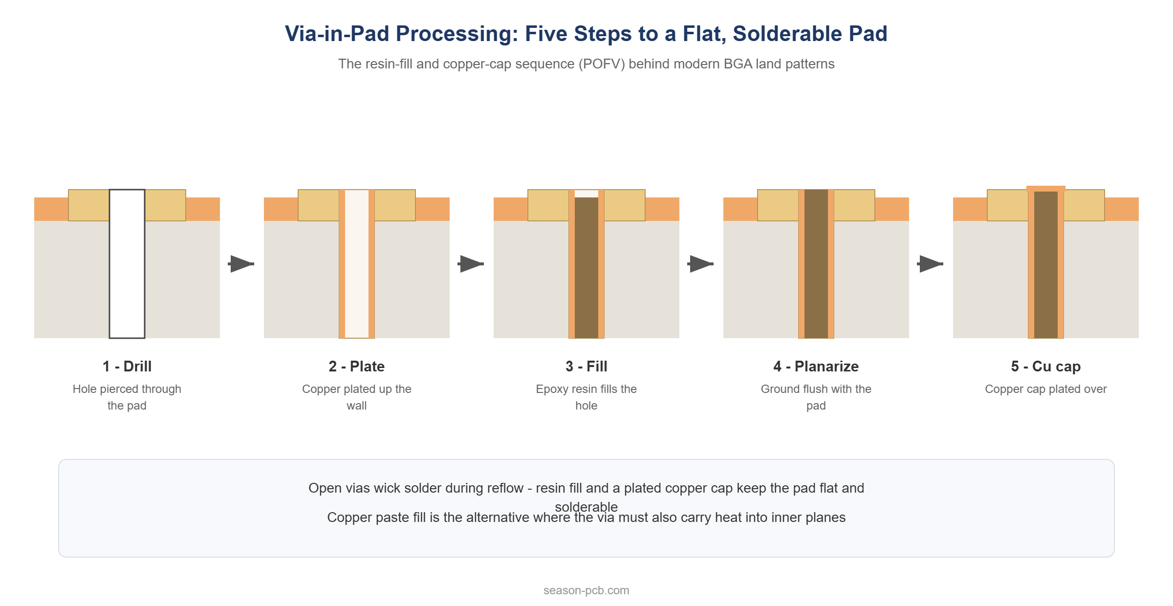
Drilling places the hole exactly on the pad centre, because a via that wanders off-centre leaves a thin crescent of pad copper after capping. Plating closes the barrel wall so the fill bonds to copper rather than to laminate. Resin is injected and cured – under vacuum on demanding builds, so trapped air cannot leave a void under the future cap. The cured resin is then ground down flush with the pad surface, and the final electroplated copper cap closes the structure. What reflow sees afterwards is a flat, solderable copper pad.
Two controls matter more than the rest. Planarization quality decides whether the stencil prints solder paste evenly – a dimple of a few microns is invisible to the eye and ruinous to the joint. And capping thickness must survive that grind with margin, which is why cap plating is specified explicitly rather than assumed. The sequence is identical whether the board is a simple four-layer design or a deep sequential build like our 14-layer computing PCB; only the tolerance tightens.
Solder Wicking, Voids and Other Failure Modes
An open via inside a pad is a small pump pointed at the joint. During reflow, molten solder drains down the plated barrel, the pad starves, and the result is a starved or lifted joint after assembly. Solder mask over the hole slows this but cannot be relied on to plug it: mask plugs crack and outgas at reflow temperatures, which is exactly why filled-and-capped structures exist.
Filled vias have their own failure mode: voids under the cap. A void hides beneath a flat surface, passes visual inspection, and turns into an intermittent or a poor thermal path after a few reflow cycles. Our article on why plating voids form in microvias covers how vacuum filling and X-ray sampling catch them before shipment.
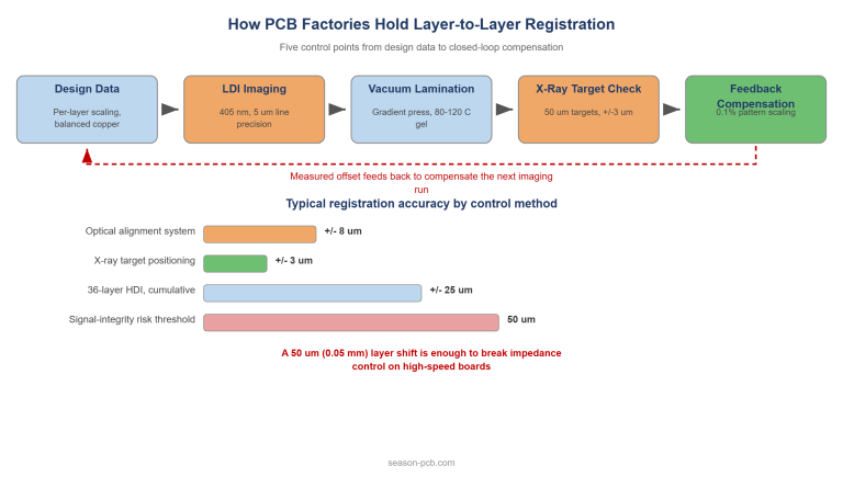
The remaining risks are process-adjacent: a cap ground too thin, resin that has not fully cured before planarization, or a pad placed half over a via that wandered off centre. All three are caught by the same discipline – defined capping thickness, verified cure, and drill-to-pad registration held at the fabricator’s stated capability rather than assumed.
Design Rules That Keep Via-in-Pad Buildable
Via-in-pad technology punishes wishful geometry. A few rules separate buildable pad vias from rework queues:
| Rule | Typical value | Why it matters |
|---|---|---|
| Via diameter vs pad diameter | Via no more than 50% of the pad | Keeps the annular ring intact through drilling and capping |
| Fill type | Resin (POFV) under BGA pads; copper paste where heat or current flows | Matches the fill function to its cost |
| Cap planarity | Copper cap flush with the pad after plating | Even stencil printing across every pad |
| Aspect ratio | 1:1 or better for filled microvias | Reliable fill without voids or thin spots |
| Solder mask | Never the primary seal over a pad via | Mask plugs crack and outgas at reflow temperatures |
One more rule sits upstream of all of these: decide where vias-in-pads are actually required. Blanket-specifying the technique across a board multiplies cost for no benefit, which is the next topic.
Cost Impact and Where to Specify It Selectively
Resin-filled, capped pad vias typically add 15–20% to the cost of the affected via compared with an open one, before counting the extra inspection. Copper paste fill costs more again. Applied to a handful of pads under one dense BGA, the board-level impact is modest; applied blanket to every via on the board, it is not.
The economic pattern that works is partitioning: resin-filled vias-in-pads under fine-pitch packages and in the dense cluster, ordinary vias everywhere the routing has room. Boards designed this way pay the process premium only where it buys escape channels or flat pads, and the standard-process majority of the board keeps the cost curve honest.
Standardization helps too. Keeping one fill spec, one cap thickness and one drill-to-pad rule across all pad vias on a panel lets the fabricator run them in a single pass, and volume production smooths the remaining premium. The technique has moved from exotic to routine precisely because that standardization matured; the via-protection structure types behind it are catalogued by the Global Electronics Association.
Via-in-Pad Technology Within HDI Stacking
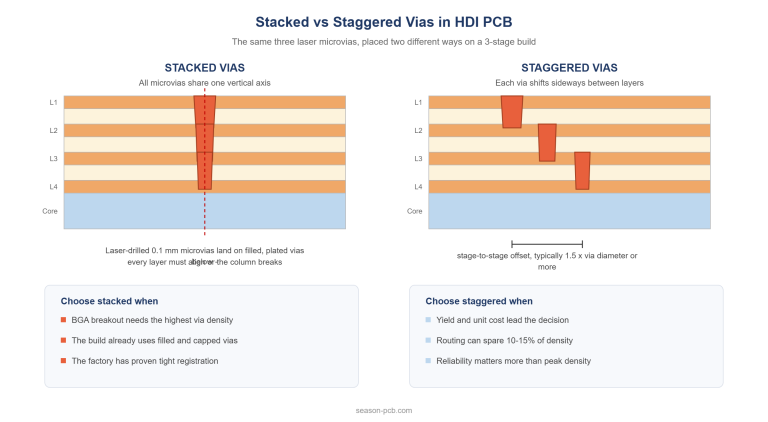
On HDI boards, via-in-pad technology and microvia stacking converge. A stacked microvia column is, structurally, a series of filled-and-capped vias on one axis – the same resin fill, the same copper cap, applied stage by stage in the build-up. Understanding one process explains most of the other, and stacked vs staggered vias shows how that column logic scales across a full stackup.
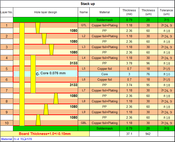
The combination is what makes dense BGA regions workable on sequential builds: pad vias connect to laser microvias, microvias stack or stagger down through the build-up layers, and buried vias carry the deepest transitions through the core. Our overview of blind and buried via HDI structures maps how those pieces fit together layer by layer, and the HDI PCB technology guide collects the design rules in one place.
The direction of travel is smaller: laser-drilled pad vias below 0.1 mm, thinner caps and finer fill control, all pushing toward pads that stay flat as features shrink. The process discipline described above is what keeps those trends manufacturable rather than merely drawable.
Frequently Asked Questions
What does via-in-pad mean in PCB design?
It means a via is placed directly inside a surface-mount pad instead of beside it. The via is drilled, plated, then filled and capped so its top becomes part of the pad surface. This reclaims the routing channels a traditional fan-out would consume, which is why it appears first under fine-pitch BGAs and in dense HDI regions.
Do all vias in pads need to be filled?
Any pad via that gets soldered on must be filled and capped; an open via wicks solder away from the joint during reflow. Vias inside non-solderable areas can stay open. On production boards the practical rule is: resin fill with a plated copper cap under every component pad, and standard open vias everywhere else.
What is POFV in PCB manufacturing?
POFV stands for plating over filled via – the standard resin-fill process for pad vias. The hole is drilled and plated, filled with epoxy resin, ground flush with the pad, and a copper cap is plated over the fill. The result is a flat, solderable pad with a working interconnect underneath, typically adding 15–20% to that via’s cost.
Why does an open via in a pad cause solder wicking?
During reflow the pad’s solder is molten for several seconds, and an open via is a connected capillary right underneath it. Surface tension draws solder down the plated barrel, starving the joint above. Solder mask plugs slow the effect but crack at reflow temperatures, so a filled, capped via is the only robust fix.
How much does via-in-pad add to board cost?
A resin-filled, capped pad via typically costs 15–20% more than an open pad via, and copper paste fill costs more again. The board-level impact depends on how many pad vias you specify – a cluster under one BGA is cheap insurance, while blanket application across a board multiplies the premium for little benefit.
Can via-in-pad be used on HDI boards?
Yes, and it is standard practice there. On HDI builds the pad via usually connects into stacked or staggered laser microvias, sharing the same filling and capping chemistry. The two techniques solve adjacent problems – via-in-pad reclaims pad-level space, and microvia stacking carries the connection down through thin dielectric layers.
How large can the via be relative to the pad?
The usual ceiling is 50% of the pad diameter: a 0.3 mm pad accommodates about a 0.15 mm via. Staying at or below that ratio keeps enough annular ring for the cap to plate uniformly and leaves the pad structurally sound through drilling, filling and planarization.
Have Your Pad Vias Reviewed Before Layout Freeze
Send your Gerber data and stackup intent, and our engineering team will mark where pad vias earn their cost, specify the fill and cap structure for each, and confirm the manufacturing plan at review. Start through our PCB manufacturing services page, or read the HDI PCB technology guide for the surrounding design rules.