Book Appointment Now

Stacked vs staggered vias solve the same problem in opposite ways. Compare structure, process demands, cost and yield before locking your HDI stackup.
Stacked vs Staggered Vias in HDI PCB: Structures, Cost and Yield
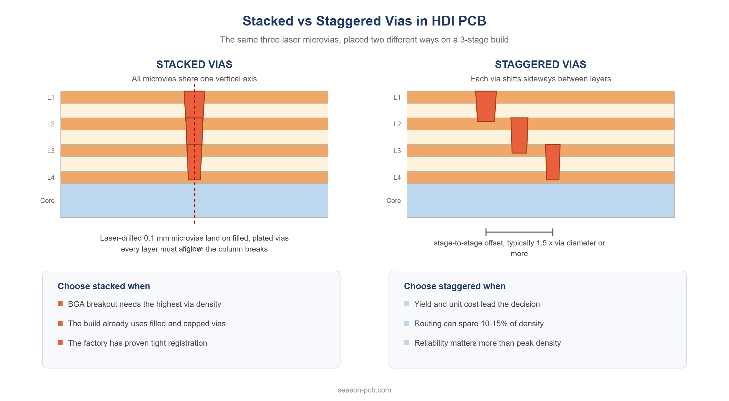
Every time a BGA shrinks or a board gets a layer denser, the interconnect question underneath it gets harder. In HDI design the two standard answers are stacked vs staggered vias: one places laser-drilled microvias directly on top of each other along a single vertical axis, while the other shifts each via sideways between layers. The choice quietly sets your alignment requirements, your filling process, your yield risk and your unit cost long before the first panel is pressed. This guide compares the two structures from a designer’s and buyer’s point of view: how each one is built, what the factory has to control, where the cost difference comes from, and when each structure is the better specification. Figures quoted here are typical industry values or our own process capability, and every build is confirmed at engineering review before production.
Table of Contents
- Stacked vs Staggered Vias: Two Ways to Interconnect HDI Layers
- What a Stacked Via Column Requires
- How a Staggered Via Layout Differs
- Registration: Where Stacked Vias Get Hard
- Via Filling and Copper Capping Requirements
- Manufacturing Steps Compared Side by Side
- Cost and Yield: The Real Trade-off
- Stacked vs Staggered Vias: How to Choose
- An 8-Layer 3-Stage Worked Example
- FAQ
- Get Your HDI Stackup Reviewed Before You Commit
Stacked vs Staggered Vias: Two Ways to Interconnect HDI Layers
Both structures solve the same problem: connecting a signal from an outer layer down through several thin dielectric layers without eating routing space. A stacked via column places two or more microvias on the same vertical axis, one directly above the other, so the connection passes straight down through the build-up layers. A staggered via layout offsets each microvia laterally, commonly by at least 1.5 times the via diameter, so no two vias share an axis and each connection changes direction between layers.
The engineering trade is density against process window. Stacked vs staggered vias differ most in what they demand from the factory: a stacked column concentrates all of the alignment and filling risk at one location, while a staggered layout spreads its connections out and tolerates a wider manufacturing window. Neither structure is better in the abstract; each buys something different with your budget.
| Attribute | Stacked vias | Staggered vias |
|---|---|---|
| Via alignment | Vertically aligned on one axis | Offset laterally at every stage |
| Routing density | Highest available in HDI | About 10–15% lower |
| Microvia diameter | 0.1 mm laser as standard, 0.076 mm reviewed per order | Same laser capability, mixed with mechanical buried vias |
| Registration demand | Tight, commonly targeted at ±15 µm between stages | Relaxed, because offset is part of the design |
| Filling requirement | Resin or copper fill plus plated copper cap, mandatory | Fill only where the stackup requires it |
| Relative processing cost | Higher, driven by fill and inspection cycles | Roughly 30% lower on processing |
| Dominant risk | Registration misses and fill voids in the column | Wider tolerance absorbs most process variation |
| Typical home ground | Dense BGA breakout, smartphone-class boards | Automotive controllers, industrial and cost-driven builds |
For a wider view of how both structures fit into sequential build-up design, the HDI PCB technology guide walks through stage counts, stackups and design rules in depth.
What a Stacked Via Column Requires
A stacked column is only as good as its weakest stage. The outer stages are laser-drilled blind vias – 0.1 mm is the production standard on our floor, and 0.076 mm is evaluated case by case – while deeper transitions may land on a mechanical buried via of 150–200 µm through the core. Each stage must land on a flat, fully filled surface, because the next drill fires into whatever the previous stage left behind.
That is why filling is not optional in a stacked build. Every via that carries another stage on top is filled with epoxy resin or copper and closed with a plated copper cap, typically at least 25 µm thick, so the next laser shot starts from a planar surface. Design rules for these microvia structures are standardized in IPC-2226, which most engineering teams use as the shared vocabulary with their fabricator.
Three preconditions decide whether a stacked column survives volume production:
- Every lower stage is filled and capped before the next stage is drilled, with fill quality verified by coupon or X-ray sampling.
- Layer-to-layer registration is held to the ±15 µm class across the whole panel, not just on the coupon.
- The copper cap thickness and flatness are controlled so the next laser via drills into copper, not into a dimple.
How a Staggered Via Layout Differs
A staggered layout offsets each microvia sideways instead of stacking it. The usual rule of thumb is an offset of at least 1.5 times the via diameter between adjacent stages – for a 0.1 mm laser via, that means roughly 150 µm of lateral separation. Because the vias never share an axis, a small registration drift between layers does not threaten the connection; it just changes where the via lands, within limits the fabricator confirms at review.
The price is routing density. Offsetting vias consumes escape channels that a stacked column would have reused, and the practical penalty is in the range of 10–15% of routing density. In exchange, the factory gains a much wider process window: filling is only needed where the stackup demands it, lamination stress is distributed instead of concentrated, and volume yields above 98% are routinely reported on staggered builds that would be ambitious as stacked columns.
Signal behaviour changes slightly too. A staggered path has a short lateral jog between stages, which adds a small discontinuity at each transition. For most clock and control routing this is noise-level; for the tightest impedance budgets it is one more reason to simulate before committing.
Registration: Where Stacked Vias Get Hard
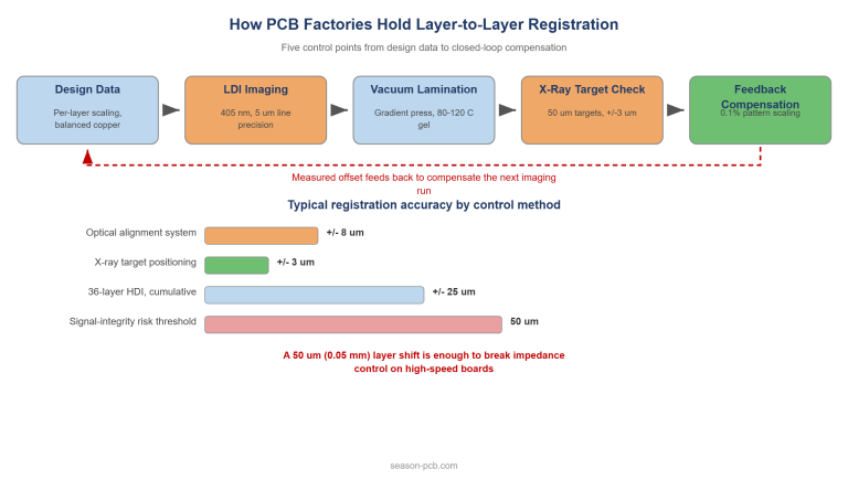
Stacked columns concentrate every tolerance in the stackup at one point. Each lamination cycle adds material movement – differing coefficients of thermal expansion between copper, prepreg and core make every layer shrink and shift by its own amount – and a stacked design has no forgiveness for the sum of those shifts. That is why serious stacked builds align each cycle against X-ray targets rather than trusting optical layer-to-layer registration alone.
The mechanics are worth understanding as a buyer, because they explain the price tag. Imaging, etch and lamination compensation are calculated per layer, targets are drilled into the panel, and post-lamination X-ray checks verify that the accumulated drift stayed inside the ±15 µm class the design assumed. Our explainer on how factories hold layer-to-layer registration covers this control loop in detail.
When you quote a stacked build, ask the fabricator for registration capability data on comparable stackups, not just a datasheet minimum. A supplier who can show measured drift distributions across a production week is telling you something a capability statement cannot.
Via Filling and Copper Capping Requirements
Filling is the quiet hero of every stacked column. An unfilled or poorly filled via traps air and chemistry; when the next stage is drilled on top of it, the result is voids, dimples or a column that cracks under thermal stress. Production stacked builds therefore specify resin fill with a plated copper cap, or full copper fill where the via also has a thermal or current-carrying job, with blind-via aspect ratios held at 1:1 or better so the fill stays reliable.
The failure mode to watch is a void under the cap: it hides under a flat surface, passes visual inspection, and only shows up as an open joint or an intermittent after reflow cycles. Our article on copper-filled vias and via filling plating explains how vacuum-assisted filling and X-ray sampling close that gap. The same chemistry sits under via-in-pad BGA pad technology, where a filled, capped via becomes the pad surface itself.
For staggered builds, filling is a design decision rather than a structural necessity. Vias that carry another stage on top still need it; independent staggered vias often do not, which is part of where the cost difference comes from.
Manufacturing Steps Compared Side by Side
The two structures share the same front end – laser drilling, plating, lamination – and diverge in how many times each step repeats and how tightly it is controlled. The table below summarizes where the effort actually goes on a multi-stage build.
| Process step | Stacked via build | Staggered via build |
|---|---|---|
| Drilling | Laser microvias per stage, drilled onto filled, capped vias below | Laser microvias plus mechanical buried vias, independently placed |
| Plating | Pulse-plated copper fill with capped columns at every stacked stage | Standard through-hole and via plating, fill only where specified |
| Lamination | One full cycle per stage, with X-ray target alignment each time | Same sequential build-up, wider alignment tolerance per cycle |
| Registration control | X-ray target verification of accumulated drift per stage | Optical alignment with the offset absorbing drift |
| Inspection load | Coupon and X-ray sampling focused on fill voids and column alignment | Standard electrical test and AOI coverage |
| Typical 8–10 layer 2-stage prototype lead time | 17–18 working days, confirmed at engineering review | Comparable cycle, fewer constraint-driven holds |
Each additional stage multiplies this effort: as a planning number, each additional HDI stage typically raises cost by 30–100% before volume learning curves. A staggered layout does not remove stages, but it removes the strictest constraints inside each stage, which is where the savings come from.
Cost and Yield: The Real Trade-off
In like-for-like stackups, a staggered build carries roughly 30% lower processing cost than a stacked equivalent. The saving comes from three places: fewer mandatory fill-and-cap cycles, lighter inspection load, and a wider process window that wastes fewer panels. Volume yields above 98% are common on staggered automotive and industrial builds, while a demanding stacked column may need engineering lots before it reaches that level.
Stacked builds earn their premium where density is the product. A column that would occupy two offsets fits in one footprint, and on a dense smartphone-class board that difference decides whether the escape routing closes at all. When it does close, the stacked premium is simply the cost of the fit; when it does not, no amount of staggering rescues the layout.
Two practical notes for quoting. First, insist on relative comparisons: fabricators that quote stacked and staggered variants of the same stackup side by side give you a real decision basis. Second, remember that lead time follows constraint density – a stack full of stacked columns books the same machines as a simpler build but holds them longer, which is where schedule risk hides. Standards context for both structures is maintained by the Global Electronics Association.
Stacked vs Staggered Vias: How to Choose
The decision usually reduces to one question: is routing density or unit cost the binding constraint? The table below maps common situations to the structure that usually wins, based on the trade-offs above.
| Design situation | Recommended structure | Why |
|---|---|---|
| 0.4 mm pitch BGA with more than two escape rows | Stacked | Escape channels stay shortest through every layer |
| 0.65–0.8 mm pitch BGA on a 6–10 layer board | Either | Density is not binding; cost and yield usually decide |
| Automotive ECU or industrial controller | Staggered | Wider process window supports long-term reliability targets |
| Any-layer HDI with a 4+N+4 build-up | Stacked | Any-layer routing depends on vertical columns between stages |
| Cost-driven consumer board with relaxed pitch | Staggered | Lower processing cost and better yield at equal function |
| Mixed-density board with one dense BGA cluster | Hybrid | Stack the dense cluster, stagger everywhere else |
Real boards mix the two more often than not: a stacked vs staggered vias decision is made per interface, not per board. Our 10-layer 2-stage HDI prototype and 14-layer 2-stage HDI prototype pages show production examples where that mix was settled at engineering review.
An 8-Layer 3-Stage Worked Example
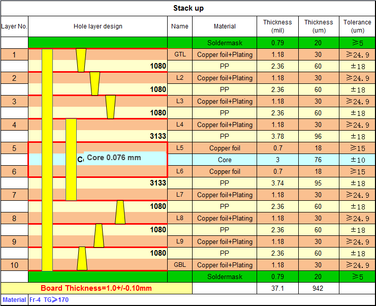
The stackup tables below come from an 8-layer, 3-stage reference build: 1.2 ±0.12 mm finished thickness over a 0.6 mm core, 1080-style prepreg between signal layers, and plated copper in the 30–35 µm range on the inner layers. The first table shows the stacked interpretation, with the microvia column sharing one axis through the upper build-up stages.

The second table keeps every material and thickness identical and changes only the via placement: each microvia lands beside the one below instead of on top of it. Copper weights, dielectric heights and the buried via through the core are unchanged – which is exactly why the two structures can be quoted as genuine variants of the same design.

For a taller example with the same logic, the 10-layer 3-stage HDI stackup walkthrough breaks the build down layer by layer, including where the fill-and-cap boundaries sit.
Frequently Asked Questions
What is the difference between stacked and staggered vias?
Stacked vias sit on one vertical axis, one directly above another, which maximizes routing density but demands tight registration and filled, capped vias at every stage. Staggered vias offset each stage sideways – typically by at least 1.5 times the via diameter – trading roughly 10–15% of density for a wider process window, lower cost and better volume yield.
Do stacked vias always need to be filled and capped?
Yes. Every via that carries another stage on top must present a flat, solid surface to the next drill, so resin fill or copper fill plus a plated copper cap is mandatory in a stacked column. Skipping the fill leaves a dimple or void that the next laser via drills into, which shows up later as opens or intermittents under thermal stress.
How much does a staggered layout save compared with stacked?
On comparable stackups, staggered processing typically runs about 30% below stacked, driven by fewer mandatory fill-and-cap cycles, lighter inspection and better first-pass yield. The exact spread depends on stage count and fill spec, so ask for both variants quoted on the same stackup – relative numbers are the only ones worth planning around.
Can stacked and staggered vias be mixed on the same board?
Yes, and it is the most common outcome in practice. Designers stack the vias where escape density demands it – usually under a fine-pitch BGA – and stagger everywhere the routing has room. The factory treats each interface according to its own filling and registration requirements, confirmed stage by stage at engineering review.
What alignment tolerance do stacked vias require?
Layer-to-layer registration for stacked columns is commonly targeted at the ±15 µm class, verified against X-ray targets after each lamination cycle. The critical number is not a single layer’s accuracy but the accumulated drift across all stages, so ask suppliers for measured drift distributions on comparable stackups rather than a single datasheet figure.
Are staggered vias worse for signal integrity?
A staggered path includes a short lateral jog between stages, which adds a minor discontinuity at each transition. For most clock, control and mid-speed routing the effect is negligible. On the tightest impedance budgets it is worth simulating, but the larger signal-integrity levers – dielectric choice, reference planes and return paths – matter far more than the via placement style.
Which structure should I choose for a 0.4 mm pitch BGA?
At 0.4 mm pitch, escape routing usually runs out of channels before cost becomes the constraint, so stacked vias are the default. If the BGA sits on a 6–10 layer board with few escape rows, a staggered variant may still close – the reliable way to know is to send the Gerber with the stackup intent and let engineering review quote both options with real process data.
Get Your HDI Stackup Reviewed Before You Commit
Send us your Gerber data and stackup intent, and our engineering team will review the stage count, filling requirements and registration assumptions on both variants – stacked, staggered or a mix – and come back with a manufacturable recommendation. Start through our PCB manufacturing services page or browse the HDI PCB technology guide for the underlying design rules.