Book Appointment Now

PCB layer-to-layer registration keeps every copper layer aligned: the methods, materials and closed-loop controls factories use to hold ±25 µm in production.
PCB Layer-to-Layer Registration: How Factories Hold ±25 µm
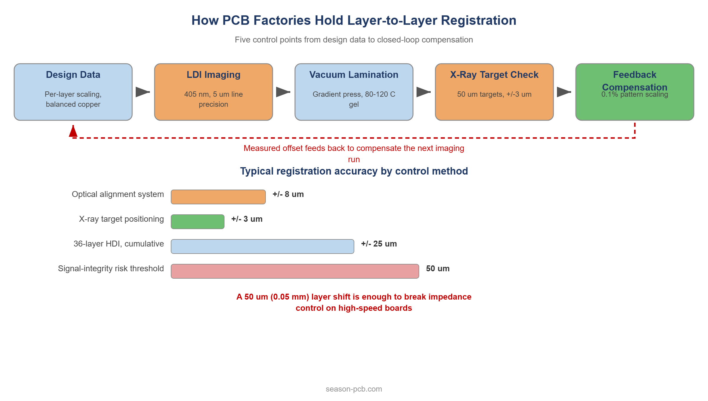
A modern multilayer board is a stack of a dozen or more independently patterned copper layers that must land on top of each other within a few ten-thousandths of an inch. When PCB layer-to-layer registration drifts by just 50 µm (0.05 mm), controlled impedance on high-speed lines can fail outright — the board looks finished, passes continuity, and still misses its electrical spec. That is why registration is one of the quiet dividing lines between a capable fabricator and a risky one.
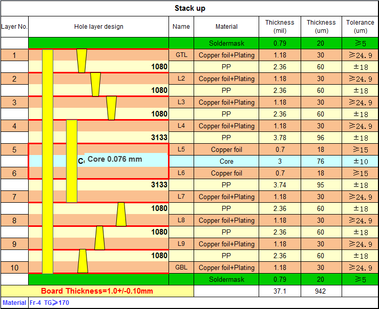
This article explains how factories actually hold that alignment: the X-ray and optical positioning systems that set the benchmark, the low-shrink materials that stop layers from moving in the first place, the lamination and imaging controls in between, and the measurement-plus-compensation loop that closes the system. If your interest is HDI specifically, the via-scale version of this problem is covered in the 10-layer 3-stage HDI stackup guide.
Table of Contents
- Why PCB Layer-to-Layer Registration Decides Board Reliability
- The Tolerance Ladder: What Good Registration Looks Like
- X-Ray Target Positioning: The ±3 µm Baseline
- Automatic Optical Alignment and Machine Vision
- Materials That Stop Shrinkage at the Source
- Lamination: Pressure, Temperature and Gel-Point Timing
- LDI: Imaging Accuracy at the Layer Level
- Measurement and Closed-Loop Compensation
- What Designers Can Do to Help Registration
- PCB Layer-to-Layer Registration in HDI Builds
- FAQ
- Have Your Stackup Reviewed for Registration Risk
Why PCB Layer-to-Layer Registration Decides Board Reliability
Registration is the offset between where a feature was designed on one layer and where it actually landed relative to the layers above and below it. Every downstream attribute depends on it: the annular ring around a via, the coupling of an impedance-controlled pair to its reference plane, the alignment of a microvia to its capture pad. None of these show up in a bare-board continuity test, which is exactly what makes poor registration dangerous — the failure surfaces later, as field returns or lab-level signal-integrity misses.
The scale is easy to underestimate. Across a 500 mm production panel, holding ±25 µm means keeping every layer within 0.005 % dimensional agreement after each layer has been etched, oxidized, laminated at roughly 180 °C and cooled at its own rate. Materials move during all of that; the registration system exists to predict the movement and cancel it out, layer by layer.
Acceptance criteria ultimately trace back to the IPC workmanship standards: undrilled annular rings, plating thicknesses and breakout limits all assume a registration capability behind them. When a quoting conversation turns to layer count and tolerance class, registration is the underlying question being priced.
The Tolerance Ladder: What Good Registration Looks Like
Different control points in the process deliver very different accuracies, and it helps to see them side by side before comparing factories. Table 1 collects the working numbers behind this article.
| Control point | Typical accuracy | Where it acts |
|---|---|---|
| X-ray target positioning | ±3 µm | Inner-layer benchmarking at lamination |
| Multi-spectral optical alignment | ±8 µm | Image-to-image registration before lamination |
| LDI pattern transfer | ≈5 µm line precision | Per-layer imaging |
| High-layer-count HDI, cumulative | ±25 µm | Whole panel, all layers |
| IC-substrate class requirement | ±5 µm | Next-generation package substrates |
| Signal-integrity risk threshold | 50 µm shift | Design-level red line |
Read the ladder from the bottom up: 50 µm of layer shift is where high-speed designs start breaking impedance budgets, so a production capability of ±25 µm keeps a two-sigma margin under the red line even for demanding builds. The ±3 to ±8 µm figures are what individual positioning systems contribute; the cumulative ±25 µm is what survives materials movement and process variation stacked on top.
When a fabricator quotes registration, ask which number they mean — a positioning-system spec and a shipped-panel guarantee are different claims. The shipped-panel number is the one that lands in your annular rings.
X-Ray Target Positioning: The ±3 µm Baseline
The backbone of modern registration is a compound system: mechanical tooling holes locate the panel coarsely, and small copper targets — around 50 µm across — are etched into each inner layer as it is patterned. Because the targets sit inside the stack, they survive lamination and can then be imaged through the laminate with X-ray, revealing exactly where each layer’s pattern ended up relative to its neighbors.
Current-generation X-ray inspection systems capture real-time imagery at hundreds of frames per second and pair it with adaptive positioning algorithms, bringing the datum-setting step to within roughly ±3 µm. That matters more than the raw number suggests: every subsequent compensation decision — drill scaling, image scaling, lamination offsets — inherits its reference from this measurement. A noisy benchmark contaminates the whole loop.
For buyers, the practical takeaway is to ask how a factory establishes layer datums on your specific build. A shop that only checks registration on coupons, after the fact, is running open-loop; a shop that benchmarks every panel through internal targets can hold tight tolerances on high-layer-count work because it sees drift while there is still time to correct it.
Automatic Optical Alignment and Machine Vision
Before layers are laminated, registration is enforced optically. The latest alignment systems image fiducial marks in several spectral bands at once — visible, infrared and ultraviolet — because different mark types and surface finishes show contrast differently. Combining the bands keeps the system reliable across copper, soldermask-covered and oxidized surfaces on the same panel.
Machine learning has changed what these systems can correct. Models trained on hundreds of thousands of production panels recognize the distortion signatures that materials leave in the marks — the systematic warping caused by thermal expansion and resin shrinkage — and compensate for them automatically rather than flagging panels for manual review. Working accuracy at the ±8 µm level, with recognition reliability above 99.9 %, is what production data from these systems now supports.
The effect compounds with exposure: when every layer is imaged against corrected fiducials, the lamination step receives a panel set that already agrees within a few microns — which is what keeps the post-lamination X-ray check a confirmation rather than a rescue.
Materials That Stop Shrinkage at the Source
Positioning systems can only compensate movement the materials have already made. The lower-leverage half of registration is therefore materials engineering: choosing laminates and prepregs that move less through the thermal cycle. Table 2 summarizes the options and what each buys.
| Material option | Dimensional behavior | Registration benefit |
|---|---|---|
| Standard FR-4 | ≈0.3 % dimensional change during lamination (resin flow) | Workable, but consumes most of a ±25 µm budget on large panels |
| Nano-silica modified epoxy laminate | Z-axis shrinkage down to ≈0.05 % | Far less post-press drift; stability holds near 180 °C processing |
| Flow-controlled prepreg (microcapsule additive) | Directional flow deviation reduced by ≈72 % | Interlayer slip held near ±15 µm |
| Glass core (TGV construction) | ≈0.01 % shrinkage | Ultra-low movement; the path to ±5 µm substrate-class work |
Two of these deserve a comment. Flow-controlled prepregs embed a three-dimensional support network of tiny thermoset microspheres that hold the glass sheets apart while the resin gels, so the layers cannot slide as the viscous resin moves — a cheap insurance policy on any build with fine registration margins. Glass cores go further still: with shrinkage an order of magnitude below organic laminates, they are the material answer when ±5 µm is the actual requirement, as the glass substrate PCB guide explains. Laminate properties across the usual FR-4 classes are compared in the PCB materials and laminates guide, and the recognition status of a specific laminate system can be verified against UL Solutions’ component databases.
Lamination: Pressure, Temperature and Gel-Point Timing
Lamination is where everything can still go wrong, because the panel is hot, the resin is liquid, and the layers are free to move until gelation locks them in place. Modern vacuum presses instrument the gap intensively — a hundred or more pressure sensing points and dozens of temperature modules map the press cavity in three dimensions, so edge-to-center differences in pressure and heat are measured rather than assumed.
The critical window is gelation, around 80–120 °C for common FR-4 systems: below it the resin flows and layers can slip, above it the resin is fixed wherever it ended up. Gradient press profiles slow the ramp through that window and relieve pressure in steps, equalizing the panel before the resin sets. Factories running this profile discipline have reported first-pass layer-alignment yield on 8-layer builds moving from around 92 % to above 99 % — the difference between a profitable HDI line and a rework shop.
Designers influence this step more than they realize. Copper balance across layers, symmetric stackups and even panel utilization all change how uniformly a panel heats and presses. A fabricator who reviews those factors at quoting time — as part of a PCB manufacturing services engagement — is protecting your registration, not just their cycle time.
LDI: Imaging Accuracy at the Layer Level
Laser direct imaging replaces film artwork with a scanning laser, and with it goes the largest historical source of registration error: film itself, with its own stretch, humidity response and aperture tolerance. Current LDI systems write at 405 nm through digital micro-mirror arrays, holding line-width precision near 5 µm across a production panel — and, more importantly, adjusting the artwork per panel.
That adjustability is the real registration feature. Because LDI writes each layer from digital data, it can scale or distort the pattern panel by panel to cancel measured material movement: the system images alignment marks, computes the actual shrinkage of that specific inner layer, and compensates the next exposure accordingly. Interferometric dual-beam setups go further, reading moiré patterns between adjacent layer images to close the loop in real time during exposure.
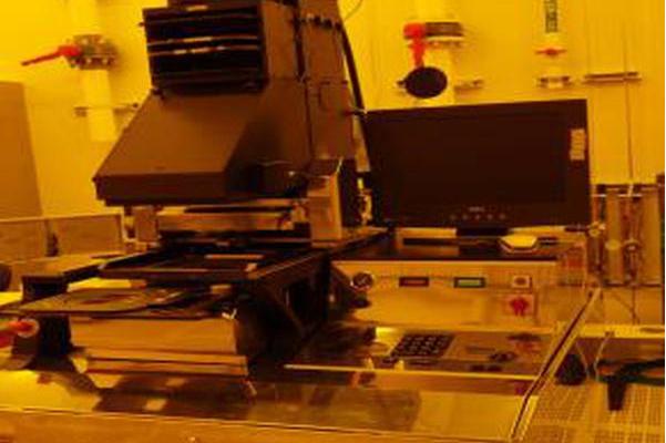
The image below shows the kind of environment this runs in — exposure equipment inside a controlled cleanroom, where temperature stability is part of the accuracy budget.
For high-layer-count HDI, production data shows LDI-based compensation holding cumulative registration within roughly ±25 µm on 36-layer constructions — precisely the tolerance ladder from Table 1. Film-based imaging cannot offer this at all, which is why layer count above a dozen effectively implies an LDI-capable fabricator.
Measurement and Closed-Loop Compensation
The last element is feedback. Three-dimensional X-ray tomography now resolves internal features down to about half a micron, reconstructing the finished board’s true layer geometry in under a minute for a high-layer-count panel. Comparing measured positions against design data produces a vector map of where each layer actually landed — the ground truth for everything upstream.
Feeding that map back into production is what turns inspection into control. When results stream into the manufacturing execution system, a systematic offset in one lot automatically adjusts the scaling applied at exposure for the next one — corrections at the 0.1 % level that quietly cancel accumulating drift. The measurement stops being a quality gate and becomes an input.
This is the loop sketched in the hero diagram of this article: design data scaled per layer, imaging, lamination, X-ray verification, and compensation feeding back into the next run. Factories that run all five elements hold ±25 µm on production HDI as a routine capability rather than a best case, which is what makes the fine via structures in modern HDI dependable in volume — and the same discipline underpins the stacked microvia work described in advanced HDI manufacturing.
What Designers Can Do to Help Registration
Registration is negotiated between design and factory, and a few habits on the design side measurably improve the odds that the finished board matches the intent:
- Keep the stackup symmetric — mirrored dielectric and copper weights let the panel laminate flat instead of bowing.
- Balance copper across layers; large empty areas laminate differently from filled ones and bias the shrinkage field.
- State registration-dependent requirements explicitly: annular ring minimums, impedance classes and BGA pitch, not just layer count.
- Size microvia capture pads for the fabricator’s demonstrated registration, not the nominal drill diameter.
- Ask for the registration data — a capable shop can produce X-ray measurement summaries for your part number.
- Lock the stackup only after the fabricator’s engineering review; late dielectric changes silently rewrite the tolerance budget.
None of these cost board space; they cost a conversation with the fabricator at the right time. On controlled-impedance and HDI builds, that conversation is usually the difference between first-pass electrical success and a respin.
PCB Layer-to-Layer Registration in HDI Builds
HDI raises the stakes because the features are smaller, not because the process differs. A 0.1 mm laser microvia on a capture pad sized for ±25 µm registration has no room for the drift a conventional through-hole would shrug off; each additional HDI stage adds a lamination cycle, and every cycle adds one more contribution to the cumulative offset. That is why the third stage of a 10-layer build is where registration capability becomes the binding constraint — the 10-layer 3-stage HDI stackup guide walks through that build in detail.
It also explains the economics. Registration capability is built from capital — X-ray systems, multi-spectral alignment, LDI, tomography — plus the process discipline to run them as a loop. A shop that has those holds fine-pitch capability without heroics; one that does not will quote optimistically and sort the difference at final inspection. When you evaluate partners for boards like a 10-layer 2-stage HDI prototype or a 14-layer 2-stage HDI build, the registration question is the fastest way to separate them. The HDI PCB technology guide collects the related process limits in one place.
Frequently Asked Questions
What is PCB layer-to-layer registration?
It is the measure of how accurately each copper layer’s pattern lands relative to the layers above and below it after lamination. Registration covers the whole chain — imaging, lamination and drilling — and is usually quoted as a per-panel tolerance such as ±25 µm on high-layer-count HDI production.
How much layer misalignment is acceptable?
It depends on the feature it affects. Workmanship standards evaluate it through annular ring and breakout limits, but the electrical bottom line is tighter: a layer shift around 50 µm (0.05 mm) is enough to break impedance control on high-speed designs. Production capability of ±25 µm keeps a safety margin under that threshold for demanding builds.
What causes layer-to-layer misalignment?
Three families of causes: materials move (laminate shrinkage and resin flow during lamination), imaging errs (artwork scaling and film distortion in older processes), and tooling drifts (panel locating and press alignment). A registration system controls all three together, because compensating one without the others just relocates the error.
How do factories measure layer registration?
Primary measurement uses copper targets etched into inner layers and read through the laminate by X-ray after lamination — accurate to a few microns. Three-dimensional X-ray tomography goes further, reconstructing the full internal geometry at sub-micron resolution in under a minute. The results feed scaling corrections back into exposure for the next panels, closing the loop.
Does registration matter more for HDI boards?
Yes, mechanically it matters more per feature: a 0.1 mm laser microvia has a much smaller capture pad than a mechanical through-hole, so the same offset consumes a larger fraction of the land. Multi-stage HDI adds a lamination cycle per stage, each contributing to the cumulative offset — which is why ±25 µm panel capability is the practical dividing line for third-stage builds.
Can designers reduce registration risk?
Keep the stackup symmetric and copper balanced so panels laminate flat; specify annular ring and impedance requirements explicitly; size microvia capture pads for the fabricator’s demonstrated registration rather than nominal drill size; and freeze the stackup only after an engineering review. These steps cost no board space and directly widen the factory’s usable process window.
How is layer registration compensated during production?
Per-panel scaling at imaging: the system measures actual shrinkage from alignment marks or X-ray data and resizes the exposure pattern — corrections at the 0.1 % level — so each layer is written slightly larger or offset to land where design data expects after lamination. Combined with flow-controlled prepregs and gradient press profiles, this holds production builds within ±25 µm.
Have Your Stackup Reviewed for Registration Risk
Season PCB (998 PCB Group, manufacturing since 2006 across Shenzhen, Jiangxi and Anhui) builds 2–30 layer boards from 1/2/3-stage to Any-layer HDI, with X-ray target benchmarking, LDI compensation and closed-loop inspection holding ±25 µm registration on third-stage production. Submit your Gerber package with layer count and impedance classes, and the engineering review returns a stackup with registration margins stated per dielectric — plus the measurement data to back them. For the via-level view of the same discipline, start from the 10-layer 3-stage HDI stackup guide.